What Are the Benefits of an LGA (Land Grid Array)?

LGA PGA BGA

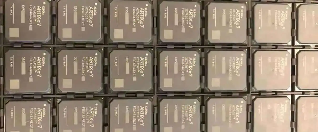
The technology of the Land Grid Array or LGA package consists of lands and an array of grid connections on the inner side of the package. The grid connection is used to connect over the surface of the PCB. However, you don’t have to use all columns and rows of a grid. The LGA socket or solder paste can help in creating connections. The elements of the grid come in various shapes and sizes. Some shapes may include polygonal, triangular, and circular. Moreover, they also appear in the pattern of a honeycomb. The design may also depend on the factors such as the electrical gap between the closeby contacts and contact likeliness instead of tolerances. This, however, gives ideal shapes and forms to the spring contacts of the counterpart, which includes the connectivity of outgoing electricity to a backplane Printed Circuit Board.

The packaging of LGA is directly associated with PGA and BGA packaging. Unlike PGA, LGA has a design that enables it to solder down with Surface-mounted technology or fit in a socket. 

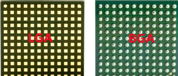
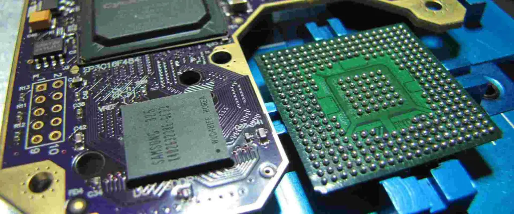
Moreover, the package of LGA does not contain any solder balls and sockets; they simply use flat connection pins which are directly placed on the PCB. Whereas the package of BGa does have soldering balls that act as connection pins between Integrated Circuits and Printed Circuit Boards. These balls are directly placed under the IC.

Why Use LGA (Land Grid Array)?

LGA-vs-BGA

The technology of surface-mount was developed in 2010, yet it has been the gold standard of the industry since then because of the following advantages.

1. Improved conductivity

The surface finish of nickel-gold prevents the device from Corrosion during storage and soldering. However, the technology enhances the conductivity and makes the associated module work optimally.

2. Footprint Optimization 

Reflow soldering may produce negative warpage. However, the unique layout of the geometric pad near the corner and middle pads removes this issue.

3. Minimal Impact On Antenna Path

LGA technology affects the path of the antenna slightly with the ground pads beneath the RF electrical components.

4. Customizable Overprinting

The size of the pad and level pitch allows customizable overprinting, which enhances the rate of yield and optimizes performance.

Installing CPU On LGA (Land Grid Array) Socket Motherboard

The surface-mount LGA packaging places the connection pins over the socket of the motherboard. It does not place them over the microprocessor. However, the design may need three steps of installation.

  1. Open the bracket of the motherboard with the metal lever.
  2. Align the microprocessor chip with the bracket accurately, along with the error margin of 2mm. Additionally, the height and max drop must remain 4mm.
  3. Close these brackets with the level and lock them safely and securely.

It works that simple way. Moreover, if you wish to take it out from the socket of the CPU, then lose the latch of the lock first. Then, take the chip and lift it in the middle with the help of your index finger and thumb.

LGA (Land Grid Array) Vs. PGA: Which Is Better?

FULL PCB MANUFACTURING Quote

Both the technology of PGA and LGA are directly related to each other as both have a reverse relationship. The technology of LGA, the chips, and IC comes in flat pads, whereas the connection puns come out from a PCB surface. Thus, this makes the PCB more sensitive to damage as the connection pins can easily break.

Whereas, in the technology of PGA, the contact pins present on the IC and the socket of the motherboard have holes that give access to the pins.

ยท Durability

The technology of LGA gives less long-lasting motherboards along with long-lasting CPUs. At the same time, the technology of PGA designs can create durable motherboards along with less long-lasting CPUs.

ยท Build Quality

The sockets of LGA are more sensitive than the sockets of PGA as they do not allow breaking the holes. At the same time, one can bend the sockets of LGA easily with little pressure, even without alignment.

ยท Space Efficiency 

The pins of PGA come smaller than their counterparts of PGA, which allows them to fit more easily.

ยท Compatibility

Intel processors use the sockets of PGA, but AMD chips seem to adopt this new technology. At the same time, PGA technology is mainly compatible with the major topology of AMD chips.

ยท Installation

Moreover, both technologies need extra care to prevent the pins from bending. Though, the installation of PGA gets easier due to sliding the pin into the holes despite attaching to the flat bottom.

LGA (Land Grid Array) Vs. BGA: Which SMT Should You Use?

The BGA and LGA both are also related to each other as both technologies offer the same features, which include easy handling, an automatic soldering process, and the automatic capability of pick-and-place.

These technologies not only share similar features but also have some different features. The technology of BGA contains connection pins between ICs and PCBs. At the same time, the technology of LGA does not contain solder balls. However, it offers flat connection points of copper that are placed over the surface of the PCB directly.

The configuration of LGA enhances flexibility, efficiency, and cost. This makes it perfect for smart manufacturing processes and mass production. Therefore, one must use PGA instead of BGA.

ยท Durability

The height of the BGA ball varies by fifty percent. Thus, this directly impacts coplanarity and functionality. Hence, apply heat to the solder balls to attach them to the surface of the device. Moreover, it may require more heating which helps in fixing the soldering balls on the surface of the module during the fabrication process of the module.

Whereas the unique PGA design helps in optimizing connections and heat dissipation. Moreover, the design also reduces the PCB warpage while reflowing the soldering process. This affects the joints from the edges and in the middle. Additionally, the finish of nickel-gold over the pads of copper enhances the durability and prevents corrosion.

ยท Flexibility

BGA 0.4 MM Pitch

In the BGA technology, apply heat to connect the soldering balls with the module. It also needs solder paste over the soldering balls, which helps them to connect over the surface of the module because already fixed solder poses a special temperature limit which further limits the heat range of solder paste.

Whereas with PGA technology, use blank pads of gold-nickel on the surface of the module. However, these pads provide greater flexibility on the customizable solder paste choice of customers. This flexibility gives full support to customers to choose solder paste according to their process and needs.

ยท Reliability

The flux residue over the surface of solder balls creates passivation as it creates a layer right above the conduction area. This layer not only affects the connectivity but also reduces the yield rate of modules and impedes efficiency. 

Whereby the optimized size of the pad in LGA technology allows customizable overprinting on the customer demands, which provides greater results. The design of pas also reduces the impact over the path of RF, whereas the flat layout optimizes the use cases of customers.

Summary

LGA refers to an ideal choice for various microprocessors because of the several useful benefits it offers. Moreover, if you want LGA technology in your IC, then contact RayPCB now.

How To Compare XC7Z020-1CLG400I With Other FPGAs?

Xilinx Artix 7

XC7Z020-1CLG400I is a highly sophisticated Field Programmable Gate Array. That’s why it is revolutionizing the way we approach complex computing tasks.  It times to discover the unique features and capabilities of this powerful device.   

The globe of electronics is evolving at a rapid pace. Every day there is innovative technology emerging all the time. One such technology that has been making waves in recent years is FPGAs. These FPGAs have revolutionized the way we approach complex computing tasks. These offer unparalleled performance and flexibility.

Although there are several FPGAs, XC7Z020-1CLG400I is an up-to-date device. It can tackle even the most demanding computing tasks. In this article, we’ll take a closer look at what the XC7Z020-1CLG400I is. How can you compare with other FPGAs? What are the key factors for comparison?

 What Is XC7Z020-1CLG400I?

 The XC7Z020-1CLG400I is a type of FPGA. FPGAs are field Programmable Gate Arrays that can perform specific computing tasks. XC7Z020-1CLG400I FPGAs are highly flexible. You can reconfigure them easily.

The XC7Z020-1CLG400I is a highly advanced FPGA due to its exceptional performance and flexibility. This powerful FPGA is a part of the Zynq-7000 family of FPGAs. They are some of the most superior FPGAs on the market today.

Features Of XC7Z020-1CLG400I

The XC7Z020-1CLG400I is a highly versatile device that offers a range of features and capabilities that make it an ideal choice for a wide range of computing applications. Some of the key features of this powerful FPGA include

  • It has dual-core ARM Cortex-A9 processors
  • Up to 85,000 logic cells as building blocks
  • Two hundred twenty DSP slices is a wonderful feature
  • One GB DDR3 SDRAM
  • High-speed serial connectivity
  • Programmable I/Os
  • 10/100/1000 Ethernet MAC
  • PCI Express Gen 2

How Does Xc7z020-1clg400i Work?

The XC7Z020-1CLG400I functions by enabling users to program the device to execute specific computational operations. It utilizes the hardware description language (HDL) such as Verilog or VHDL. Upon completion of programming, the device can execute the computational tasks. Since FPGAs are exceptionally adaptable, the programming is modified by accommodating or shifting computational demands. The XC7Z020-1CLG400I’s dual-core ARM Cortex-A9 processors are a significant benefit, as they offer remarkable performance and efficiency. In addition, it is an optimal choice for strenuous computational applications.

Key Factors To Keep In Mind While Comparing XC7Z020-1CLG400I With Other FPGA

FULL PCB MANUFACTURING Quote

 Sometimes it’s necessary to compare different FPGAs to choose the right one. If you choose the wrong FPGA, it will destroy the whole concept. That s why it is necessary to keep certain apartments in mind.

When it comes to comparing the XC7Z020-1CLG400I with other FPGAs on the market, the following are the key factors to look at.

1. Performance

 Performance is the main key factor. Do you know why designers and engineers go for XC7Z020-1CLG400I? It is exceptional in its exceptional performance and processing speed. With up to 85,000 logic cells and 220 DSP slices, this powerful FPGA is just amazing. That’s why it can easily handle even the most demanding computing tasks. When compared to other FPGAs on the market, the XC7Z020-1CLG400I often comes out ahead in terms of performance. Still, there are some FPGAs that are great or even better performance. That’s why some people get confused. As a result, they decide or choose the wrong one. But XC7Z020-1CLG400I is one of the top-performing FPGAs available today. In addition, it offers great processing performance in all aspects.

2. Flexibility For Customization

How flexible are your FPGAs as compared to other FPGAs? This is an important factor when making a comparison. The XC7Z020-1CLG400I offers great flexibility. All FPGAs are reconfigured easily but every FPGA has limitations in reconfiguring. They also have reconfiguring capacity. XC7Z020-1CLG400I offers a great level of flexibility that traditional 

FPGAs and integrated circuits simply can’t match. You compare it with other FPGAs, the XC7Z020-1CLG400I shows greater reconfiguring capacity. That’s why it is an ideal choice for applications where flexibility is key. For example, industrial automation and communications have the best place for this FPGA. That’s why it is necessary to focus on the flexibility of both the FPGA. Always go for the better flexibility FPGA. Flexibility for reconfiguring is the must option to compare. You have to recognize FPGA several times during work.

3. The Need And Requirements

ย All FPGAs are not equal. Every FPGA has up and downsides. That’s why a detailed comparison is necessary. Moreover, when comparing XC7Z020-1CLG400I with other FPGAs, then must keep in mind your need and requirements. XC7Z020-1CLG400I FPGA mostly fulfills the demand of designers. If you choose an FPGA that doesn’t meet the needs, then you will lose the game. As a result, you cannot achieve desired outcomes. That’s why it is important to compare your selected FPGA and some available FPGAs for better results.

4. Price Comparison

 Price is the last key factor. Yes, price matters, but FPGA’s qualities also matter. No doubt price is always an important factor to consider but keep in mind your need also. What do you expect from FPGA? Sometimes you choose FPGA that doesn’t suit your need. As a result, you are unable to achieve your objectives. While the XC7Z020-1CLG400I is certainly a powerful and versatile FPGA but it is on the higher price side. Some people don’t like it due to its price, and they go for cheaper options having similar properties.

However, for applications where performance and flexibility are a top priority, the XC7Z020-1CLG400I is ideal. That’s why don’t compromise quality features over price.

 Wrapping Up the Things

Overall, the XC7Z020-1CLG400I is a modern and versatile FPGA. That’s why it offers exceptional performance and flexibility. It is more expensive than some other FPGAs on the market. But its unique features make it an ideal choice for a wide range of computing applications.

When you compare it with other FPGAs, the XC7Z020-1CLG400I often comes first. Because its performance and flexibility are superb, it’s important to carefully consider your specific needs before purchasing. Above all, XC7Z020-1CLG400I FPGA is useful for many needs and comparatively better for different tasks.

Your Perfect Guide to XCKU060-1FFVA1156C

Xilinx Zynq

FPGAs are the heart of every modern electronic device. That’s why every sophisticated and modern device has an FPGA. If you are into electronics and circuits, then you must know about FPGAs. These FPGAs are versatile and easily configured according to need. As a result, their popularity is increasing day by day.

What Is XCKU060-1FFVA1156C?

Xilinx is a leading provider of FPGAs and logic devices around the globe. FPGAs are electronic components that are easy to program and reprogram to perform specific functions. The XCKU060-1FFVA1156C is one of the most popular FPGAs in the Xilinx product line. That’s why designers and engineers like it. Its unique features make it an irresistible component of any system

Here Are the Specifications of XCKU060-1FFVA1156C

  • This FPGA has 580440 logic cells. As you know, logic cells are the building blocks of an FPGA.
  • This FPGA has 624 inputs and puts pins. That’s why it is easy to integrate with other systems.
  • Number of CLB in this FPGA is 2760.
  • It supports ROHS3 Compliant system
  • These specifications make XCKU060-1FFVA1156C a high-performance FPGA device that can handle complex tasks in various applications.

Break Down the Alphanumeric Code XCKU060-1FFVA1156C.

For many people, these are ordinary alphabets or numbers. Actually, it is not true. Every alphabet and number has some significance and gives you information regarding FPGA. As a result, you can have basin information regarding FPGA.

Sure, let’s break down the alphanumeric code of XCKU060-1FFVA1156C:

  • Every FPGA belongs to a specific family due to its certain characteristics. Here XCKU060 represents the Kintex UltraScale+ FPGA family. Furthermore, The 060 indicates that it has 
  • Sixty percent of the maximum capacity of the family.
  • 1FFG1156 represents the package type. 
  • In addition, it represents the number of in and output pins, package size, and other specifications. 
  • FF represents the package type and size.
  • 1156 represents the number of Input and output pins in this FPGA.
  • C represents the RoHS compliance code and indicates that the device is compliant with the “European Union’s Restriction standards.

Overall, the alphanumeric code of XCKU060-1FFVA1156C provides important information about the device’s family-specific model, package type, and compliance status. That’s why designers and engineers give importance to the specific part number.

 Eminent Features

 The following features make it eminent among all other FPGAs.

1. Monolithic And Next-Generation Technology

 Do you know what is special about this FPGA? This FPGA XCKU060-1FFVA1156C is manufactured on the latest h monolithic and next-generation stacked silicon interconnect technology. You can expect high performance from this particular FPGA. It offers a high level of integration with other systems. In addition, its life expectancy is long, so you can expect more from it. This FPGA has a longer life span, so you can expect it will save repair costs in the future too. Overall, it is a good package FPGA.

2. High-Performance Configuration

 This FPGA has excellent specifications. It has good enough RAM for data storage. Similarly, it has high-performance configuration blocks. These blocks make it enable the configuration from external media.

 It also supports various other protocols. For example, it supports PCIe and easily does configuration without any inconvenience. Sometimes this configuration block provides some additional unencrypted configuration. It has a fairly good amount of DSP slices and a better clock management system. Overall, it is the best FPGA due to its ideal specifications.

3. Optimum Blend Of Capability And Cost

ย It is really hard to find a good FPGA with great features. If you look at the specification of this FPGA, then you come to know that it is the optimum blend of capability and cost. Yes, it offers you high DSP and blocks RAM-to-logic ratios. In addition, its next-generation transceivers, combined with low-cost packaging, enable you to do what you want. You can achieve an optimum blend of capability and cost without going beyond your budget. So I would recommend you go for this FPGA to make your dream system integration possible.

4. Footprint Compatibility with Migrating Devices

 When we have to transfer data from one device to another, there are several technical issues.

 This FPGA provides footprint compatibility to facilitate users to migrate designs from one device or family to another without any tension. Any two FPGAs with the same footprint identifier code are footprint compatible. This feature is quite feasible for many new designers and engineers.

5. Packaging Type

This FPGA comes in tray packaging based on surface mount technology. In addition, this FPGA has

CBGA, aka Flip Chip Ball Grid Array packaging. It is a type of modern packaging technology. In this way of packing active ends of components, rare down face. In this case, 1156 is the number of balls.

6. Operating Temperature

Operating temperature means the optimum temperature at which FPGA can work efficiently. For this FPGA, this temperature range is between 0ยฐC to 85ยฐC. This shows that this FPGA can function even in harsh environments. There are some FPGAs that can tolerate -41 to 100ยฐC. But this is, again, a fairly good temperature range for this FPGA. In addition, it has a great moisture sensitivity level that is 72 hours.

 What Is The Difference Between Xilinxxcku060-1FFVA1156C And Xilinxxcku060-1FFVA1156I?

FULL PCB MANUFACTURING Quote

 Both FPGA belong to the same family, so they share some common specifications. For example, both offer higher performance. Both are budget-friendly. Similarly both offers your energy or power saving. But they also have differences in their temperature tolerability range. XilinxXCKU060-1FFVA1156C’s temperature range is 0 to 85 centigrade, while XilinxXCKU060-1FFVA1156I tolerates -41 to 100ยฐC. Overall, both share the same features. So if you want to choose any one of them, then check your temperature requirements.

 Wrapping Up the Things

I hope now you have a better understanding of this FPGA. This FGA has unique features and belongs to the Kintex UltraScale family. This family is famous for its unique features and great FPGA fabric. I also tried to explain the specifications in a simple and easy manner. That’s why if you are looking for the preeminent FPGA for your next project, then you must go for this FPGA. Otherwise, you may regret later for not taking this decision.

What Processes Go into Medical Device Contract Assembly?

Medical Electronics

Medical device contract assembly manufacturing refers to the bulk production of medical devices, such as digital thermometers, ultrasound imaging, glucometers, and heart rate monitors.

The medical device contract manufacturer uses a wide range of processes to make these devices. Some of the processes include injection molding, ultrasonic welding, CNC machining and laser marking.

In this article, you will find out some of the important pieces of information about medical device contract assembly.

What is Medical Device Contract Assembly?

It refers to the series of production processes that an electronic manufacturing company uses to manufacture devices for the medical industry. However, it is not a straightforward process, because two different parties are required for the assembly to happen.

The Medical Device Company

The medical device company needs to contract a contract manufacturer for the job. This is done to help the company transform its medical device ideas to the manufacturer to produce, according to the specifications.

The Contract Manufacturing Company

The work of the Contract Manufacturer (CM) is to take the medical companyโ€™s orders and make sure that the specifications are met.

Ideally, the Contract Manufacturing (CM) process allows for the manufacturing company to make or produce either the medical device components or the medical device itself. Either way, the job of the CM is to manufacture these items and have them shipped to the medical company for usage or resell.

Why Do Medical Device Companies Reach out to Contract Manufacturers?

Medical Devices PCBA

The contract manufacturing companies are called upon to produce these outsourced medical devices and related components for some reasons.

First, it is because the medical device companies either have limited facilities, equipment or the technical know-how to produce these devices and the components.

Second, the Contract Manufacturer (CM) is hired because of the experience, streamlined process and improved design it offers.

Generally, the medical device companies want to work with the CM for the following reasons:

  • Convenience
  • Maintenance of quality control
  • Flexible medical device production and;
  • Flexible payments for the manufactured devices.
  • Medical device Contract Manufacturers (CMs) are also contracted because of the excellent management of the devicesโ€™ upgrades.
  • The need to stick to the industry standards and regulatory guidance is also another reason.

What Does the Medical Device Contract Manufacturer Do?

The manufacturer handles anything from designing, developing, testing and shipping the medical devices.

Here is a breakdown of the medical device CMโ€™s job description:

1. Supply Chain Management

On getting the orders from the Original Equipment Manufacturer (OEM), the contract manufacturer proceeds to procure the components for the job.

Often times, the CM has access to an extensive network of component suppliers. This gives the medical device company (the OEM), better deals, in terms of affordable components and quality standards.

In addition to negotiating for better rates and sourcing the best components, the CM also handles the real-time shipping of the completed devices.

Other aspects of the supply chain that the medical device Contract Manufacturer (CM) handles are:

  • Production schedule management
  • Hiring and contracting of talents, such as engineers, assembly workers and technicians.
  • Managing the lead time or delivery timeframe.
  • The provision of warehousing facilities for the devices.

2. Design and Development

Once the components or parts are sourced, the CM starts working on the initial designs or prototypes. The company, on the completion of the designs, starts developing the โ€œworking versionโ€ of the medical devices.

The following are some of the scopes of the design and development:

  • Sterilization
  • Small-scale or prototype productions
  • Welding
  • Packaging

3.ย Regulatory and Compliance Assistance

FULL PCB MANUFACTURING Quote

The medical device CM also helps the OEM with meeting the requirements for the medical devices. These include meeting the minimum industry standards and guidelines set by the Food and Drug Administration (FDA).

The following are some of the standards and guidelines:

  • ISO:13485: This spells out the quality certification of the medical devices. In addition, this standard also specifies how the structure of the devicesโ€™ quality management should be. The ISO:13485 standard also specifies different provisions, such as monitoring, product realization planning, measurement, production, design, component sourcing and medical device development.
  • ISO:14971: This standard has to do with the medical devicesโ€™ risk generation and execution plans.
  • FDA 21 CFR Part 807: This spells out the registration of all the parties involved in the production and distribution of the medical devices.
  • IEC 60601: This spells out the safety requirements for the electrical medical devices.

Based on the FDA guidelines for medical device production, all Contract Manufacturers (CMs) are required to:

  • Meet up with the changing requirements for the production of medical devices.
  • The CMs are also required to have standardized equipment and procedures for the production of medical devices.

4. Class-Centric Compliances

Medical devices are categorized into classes, based on the usage, with Class III devices being the most-regulated.

The medical device contract manufacturing assembly is required to meet the minimum requirements of these classes, as well as having the capabilities to meet the increased constraints.

5. Quality Compliance

This is where the Contract Manufacturer (CM) is expected to meet the medical devicesโ€™ quality standards. Quality-related issues can be addressed via the following measures:

  • Sticking to meeting the minimum quality requirements for the medical devices.
  • Testing and validating the devicesโ€™ performance.
  • In addition to inspecting the medical devices, it is also imperative for the CM to identify areas that need improvements during the production phase.
  • The ISO:13485 guidelines are required here for the following purposes: process validation using protocols like PQs, IQ and OQ; and ensuring the medical device componentsโ€™ quality.

6. Design Upgrade

The Original Equipment Manufacturer can also hire the Contract Manufacturer to upgrade the existing designs. This becomes imperative when there is a new competing variant of such devices, and when there is a need to refine the design and manufacturing process of the device.

7. Setting-Up On-Site Medical Labs

The medical device Contract Manufacturer (CM) needs to have a combination of on-site labs and on-site engineers. Having this two helps the manufacturer to achieve the following:

  • Validation and verification of new medical devices.
  • Real-time facilitation and implementation of necessary design changes.
  • Establishment and usage of cleanrooms. These rooms serve a variety of purposes, such as utilizing hermetical sealing, and specialized clothing for keeping the medical devices free of contaminants.

The Medical Device Contract Manufacturing Process

medical pcb assembly

For the Contract Manufacturer (CM) needs to discuss with the OEM before any further step is taken. Here is a breakdown of the steps involved in the contracted or outsourced process of manufacturing medical devices:

Device Prototyping

Depending on the specifications the OEM provides, the CM will start working on the early-stage designs (prototypes). This is done to get a โ€œblueprintโ€ that serves as a basis for building the rest of the device, as well as saving costs.

The prototype has to be realistic, comply with the existing standards and be scalable.

Prototype Expansion

Expanding the prototype means building it based on the changes made. It also involves the development of the medical devicesโ€™ components, using any of the following processes/techniques:

  • Electrical Discharge Machining (EDM)
  • Injection molding and;
  • CNC machining/milling

Medical Device Production

The production goes both ways: manufacturing and assembly. The former is done first before the latter, where the components are assembled or placed on the device.

Other processes that go into medical device production are:

  • Pad Printing: this is the process of giving unique identifiers and markings for the devices. Examples are engraving serial numbers, barcodes and logos.
  • Soldering: it entails the joining of multiple metals via the melting of one of the metals into the other metalโ€™s joints.
  • Ultrasonic Welding: this is a systematic process of joining several plastic medical device parts, without having to use either adhesives or solvents.

Medical Device Packaging

The medical devices must be packaged or packed in accordance with the FDAโ€™s guidelines. The goal is to validate the compatibility of the package with the medical device.

Medical device packaging options cut across pouches, childproof usage, blister packaging, header bags and smart packaging.

Supply Chain Management

Covered here are the shipping and Product Lifestyle Management (PLM). The PLM has to do with the medical device contract assembly companyโ€™s capabilities to manage the supply chain (components sourcing and device shipping), upgrades to the existing designs and coming up with commercialization strategies.

How OEMs Benefit from Medical Device Contract Assembly

Medical device companies tend to benefit a lot from hiring a Contract Manufacturer (CM) to handle their products designs.

Here are the different advantages to this arrangement:

Expansion Capabilities

The CM can help you expand the line of medical devices, especially if you intend on creating competitive devices.

Depending on the manufacturerโ€™s scope, your medical device company could benefit from expanding the distribution to newer territories.

Savings All the Way

From buying and maintaining specialized equipment; the cost of producing medical devices is higher.

By using the services of a professional Contract Manufacturer (CM), your company tends to save costs.

The cost-saving mechanisms include:

  • Cleanroom Requirements: building and maintaining cleanrooms come at some additional expenses. Your medical device company is better off hiring a Contract Manufacturer (CM) to help save costs on building and maintaining a cleanroom.
  • Reduced Production Costs: the costs of producing the medical devices are considerably lower if you are using a CM. You get to optimize the costs across the following facets: costs of acquiring relevant machinery, resource costs and costs of procuring the device components.
  • Regulatory Assistance: your medical device Contract Manufacturer (CM) also helps to certify the devices as per the several regulatory policies. Besides, satisfying these policies can also aid the expansion of your companyโ€™s medical devices to newer markets.

Experience to Upscale

Your medical devices will benefit from the Contract Manufacturer (CM)โ€™s years of experience. This is a major boost towards the upscaling and upgrading of the devices across different segments.

Quality Compliance

Since most medical devices are directly used for different life-related activities; they need to be safe. Thus, the ability to meet the different quality compliance is a major benefit of working with a Contract Manufacturer (CM).

In addition to modifying the devices according to the industry standards and FPA guidelines, we also make an individual testing of the devices. In the event that design-related and quality issues are noticed, we would fix those before finalizing the devicesโ€™ final design.

Medical Device Contract Manufacturer Selection Guide

Medical Surgery
Medical Surgery

Choosing the best company for designing and assembling the devices come with a lot of brainstorming sessions. How about we take away the guesswork and intimate you with the factors to look out for?

1. Manufacturing and Assembly Process

The Contract Manufacturer (CM) should have an agile manufacturing and assembling process for the medical devices.

This provides for faster production, transparency, reduced risks of board quality issues and development of quality medical devices.

2. Production Capabilities

The CMโ€™s production capabilities range from the type of equipment used, the production capabilities, such as low, medium and high-volume orders.

3. Excellent Supply Chain Management

The CM is there to make the job easier for your medical device company. The efforts made in this regard include sourcing for the components, reducing the lead time and overseeing the devicesโ€™ shipping.

4. Consider the Medical Device Assembly Capabilities

The Contract Manufacturer (CM) should also exhibit the capabilities to enable functional assembly of the medical devices.

Here are some of the efforts to expect in this regard:

  • Automated equipment can be used to make the process seamless and drive down costs of manual labor.
  • The Contract Manufacturer (CM) may also want to migrate some existing product lines to design yours. This works best if the previous product lines have been proven efficient.

5. Transparency

Your Contract Manufacturer (CM) should be able to keep you in the know of the latest details of your medical device.

From having an open communication channel to being clear about the processes used; the manufacturer should be able to carry you along.

Final Words

The medical device contract market continually expands due to the advanced technologies that improve the way medical devices are produced. To produce the best of these devices and to have the target audience get value from it, do not hesitate to work with a professional Contract Manufacturer (CM).

Importance of Microwave and Radar Engineering in Todayโ€™s World

Microwave and radar engineering

Microwave and radar engineering is a great aspect of engineering. It involves the design and testing of microwave circuits, components and radar systems. The basic principles of microwave and radar engineering are usually applied to design and analysis in this field. Also, microwave and radar have made positive impacts in several applications.

Microwave and Radar Definition

Microwaves are electromagnetic waves with frequency within the range of 1 GHz and 300 GHz. You can transmit microwaves as a beam signal in given directions since they have smaller wavelengths. Also, the path of microwaves remains the same when they collide with any object. Although microwaves can have a reflection from the object, their path remains the same. Due to this capability, microwaves are ideal for use in radar.

Radar means Radio Detection and Ranging. The radar system helps to detect the direction, presence, velocity, and distance of an object in motion. Also, this device can detect stable objects. The transmitter of a radar transmits the microwaves in every direction. The object reflects the microwaves and the microwaves are received. Therefore, radar is a good device for detecting an object.

Microwaves are commonly integrated in radars since they are capable of passing through an object. The microwavesโ€™ frequency is between radio waves and infrared waves. The frequencyโ€™s range of microwaves can help in detecting fast-moving objects such as ships, aircraft, and rockets.

Furthermore, microwaves are useful in radar as they help in detecting objects such as missiles, ships underwater, and aircraft. The radar in ships transfers the microwaves in water to detect any motion under water.

What is Microwave and Radar Engineering?

From the above explanation, we understand that microwaves and radar work hand in hand. Microwaves are useful in the radar system due to the functions they offer.  Microwave and radar engineering involves the design and testing of microwave circuits, components and radar systems. The basic principles of microwave and radar engineering are usually applied to design and analysis in this field.

Furthermore, microwave and radar engineering involves building and testing radar systems, microwave components. From the creation of complex formulas to selecting materials as well as components utilized in constructing microwave and radar, a microwave and radar engineer requires skills to carry out their responsibilities.

Radars are capable of powering different operations such as tracking and forecasting. Regardless of the function of the radar, radars require round-the-clock adjustment to function well. Therefore, as a microwave and radar engineer, you need the necessary skills and expertise to perform your task.

During the second world war, microwave engineering contributed to the development of radars which helped in locating planes and enemy shops. A microwave and radar engineer oversees team members in some specialties, Fixing technical bugs, and developing mathematical analytics are important tasks you have to carry out.

Microwave and radar engineering has become relevant in our world today. This is because the microwave and radar domain has moved into the commercial sector. Microwave and radar systems are not only useful to military technologies used in the 20th and 21st century.

Furthermore, digital communications and inexpensive components in the microwave and radar domain have helped to discover areas associated with this discipline. These areas include wireless radio, collision avoidance radar, and satellite.

What does a Microwave and Radar Engineer Do?

A microwave and radar engineer needs to undergo some training and must have a good knowledge of what microwave and radar engineering entails. This is because these engineers are usually saddled with a lot of responsibilities. As a microwave and radar engineer, you will be tasked with the responsibility of designing, manufacturing, and repairing microwave and radar devices. You may need to work with computer programs to work on some possible product designs and as well test these designs for quality and performance.

Also, you will have to work with a team to work on some project. A microwave and radar engineer monitors the microwave and radar system and works on theories to enhance their performance. These engineers need to undergo a program in microwave and radar engineering.

Radar engineers carry out tests on various combinations to be sure which would enhance the accuracy of the radar and which isnโ€™t functional.

To become a microwave and radar engineer, you need to study a course in this field. There are different universities as well as colleges, which offer this course. Take for example, University of Massachusetts offers programs in microwave, remote sensing, and radar systems. Asides from acquiring educational qualification, a microwave and radar engineer must have problem solving skills, communication skills, and analytical skills.

Aside from getting a degree in microwave and radar engineering, it is important for microwave and radar engineers to need some basic skills like problem solving, effective communication, critical thinking, and leadership. Microwave and radar engineers are tasked with the responsibilities of solving complex problems.

Engineers need to be able to discover opportunities and create innovative ideas. Also, leadership is a crucial role for microwave and radar engineers as they would be working with a team.

Why is Microwave and Radar Engineering Important?

FULL PCB MANUFACTURING Quote

The microwave and radar technology is important in todayโ€™s world. It is responsible for a lot of development in various sectors. For instance, the radar system guides the transportation of clothing and gadgets at our ports. Microwave and radar engineering is a special field within electrical engineering. This engineering field deals with components and systems that operate in microwave and radar.

Radars can detect spacecraft, and as well track aircraft. They can measure the speed of automobiles and properties of the oceans. Microwaves are considered useful in radars because they offer high resolution of the target. This is possible due to the shorter wavelengths of microwaves. With shorter wavelengths, microwaves can bounce off in such a way that smaller aircrafts can easily detect them.

Different radars integrate different wavelengths in order to resolve various kinds of objects. Microwave and radar engineering play a crucial role in various applications. While a radar gun can send a burst of microwaves. Microwaves can be reflected from the oncoming vehicle and the receiver in the radar gun can detect the oncoming vehicle.

Microwave and radar engineering have helped in the development and testing of microwave and radar components.  This field of engineering is crucial for the development of modern devices. The microwave and radar technology is a remote object detection system that images the ocean, space, and terrain to identify objects, forest, land cover, and more.

Applications of Radar

The radar technology has found its use in several applications. Below are applications of Radar:

Air traffic control

Radar is used in controlling air traffic around airports. For instance The Air Surveillance RADAR can identify and reveal the position of aircraft in the airport terminals. Furthermore, Radar guides aircraft on where to land during bad weather. With the help of the radar technology, it is easy to scan for ground vehicle and aircraft positions.

Space

Radar plays a crucial role in space. It guides space vehicle on how to land safely on the moon. Also, it helps in observing planetary systems. With Radar, you can monitor satellites and meteors.

Military

Radar is very useful in military applications. It is mainly used for the purpose of surveillance. With the surveillance radar, you can detect and locate enemy targets. Furthermore, the radar technology is integrated for supplying navigation aids to military and civil aircraft. Radar can help to control weapons and trace targets.

Remote sensing

Radar can observe planetary positions and as well monitor sea ice. This enables a good and smooth route for ships.

Applications of Microwave

Microwave Engineering

Microwave is crucial in some applications as it plays vital roles. It is commonly used for wireless transmission. Also, it is suitable for use in radar systems since radar integrates microwave radiation to identify distance, range, and other properties of mobile broadband and sensing devices.

Another application of microwaves is in radio. In this case, microwaves broadcast and telecommunicates the transmission since their wavelength is very small. Also, microwaves have proved useful in telephones as they ensure long-distance communication.

Furthermore, a rare use case of microwaves is in the biomedical field. In this application, the microwave is used for LASER therapy and thermotherapy for the treatment of cancer cells. In the medical field, microwaves have been used for several treatments. The microwave technology has helped in the successful treatment of certain illnesses and diseases.

Microwave is also a great option for curing and drying products. The microwave oven is a household appliance used for food preparation. The microwaveโ€™s high energy rotates the molecules of sugar, fat, and water in the food. As a result of this rotation, there is friction. The friction causes heat generation.

Conclusion

Microwave and radar engineering is another field in the engineering sector. In this engineering field, professionals are needed. Microwave and radar engineering involves building and testing radar systems, microwave components. Also, microwave and radar engineering has become relevant in our world today. This is because the microwave and radar domain has moved into the commercial sector.

What is the Significance of Solder Paste Printing?

Solder paste printing

The application of solder paste is one of the most crucial processes in the SMT assembly. This process requires careful attention and a high level of precision. This is because the main goal is to apply solder in the proper location and adequately. Therefore, it is important to carefully coat each pad using the appropriate amount of solder.

The most common method integrated is screen-printing the solder paste. Solder printing is the most delicate step in the printed circuit board assembly. Printed circuit boards have defects due to the use of poor methods and tools for applying solder paste.  Solder paste containing lead are not RoHS compliant. It is advisable to apply lead-free solder paste on printed circuit boards.

Rayming PCB makes use of automatic solder paste printers and a squeegee blade to apply solder paste on a circuit board. Also, this PCB assembler ensures enough pressure is applied to completely cover the circuit board with paste by dragging a squeegee blade through the pcb stencil printer, which has been tailored according to the IPC-7525A. These blades are typically made of metal. Here is a list of the key elements that determines effective solder paste printing.

What to Consider During Solder Paste Printing

smd soldering paste

Squeegee Speed

The amount of time the solder paste has to “roll” in the stencil’s apertures as well as onto the PCB pads is determined by the speed at which the squeegee travels.  The standard setting is 25 mm every second, however, this varies according to the aperture size within the solder paste and stencil used.

The Squeegee Pressure

To guarantee a thorough wipe of a stencil throughout a print cycle, it’s critical to apply enough pressure over the whole length of your squeegee blade.  Inadequate pressure might lead to incomplete transfer into the PCB, inadequate deposition, and “smearing” of that paste onto the stencil.  When there is too much pressure, this can cause paste “bleeding” between the PCB and stencil, “scooping” paste from bigger apertures, and too much wear from the squeegees and stencil.  A normal setting for the pressure of the squeegee is 500 grams for every 25mm of the squeegee blade.

The Squeegee Angle

Those holders to which the squeegees are attached usually set their angle at 60 degrees. If there is an increase in angle, the solder paste deposited will be minimal since the paste will be “scooped” out of the stencil apertures. Any reduction in the angle may result in solder paste residue remaining within the stencil once the squeegee concludes printing.

Speed of Stencil Separation

The speed of stencil separation describes the rate at which the circuit board gets separated from its stencil.  The apertures’ size within a pcb stencil printer will determine the speed setting, which can range from zero to three millimeters per second.  If this happens too quickly, the solder paste won’t completely release from these apertures, and “dog-ears”โ€”high edges surrounding the depositsโ€”will appear.

Cleaning the Stencil

Cleaning the stencil needs frequently is recommended while it is being used; the PCB assembler can perform this manually or mechanically.  A good number of automatic printing devices feature a system you can configure to clean a stencil using lint-free material and a cleaning agent such as IPA after a using a certain amount of prints.  The system executes two main tasks which is it cleans the stencil’s underside to prevent any form of smudging, and again it makes use of suction to clean off the apertures to prevent any form of obstructions.

Squeegee and stencil condition

soldering flux paste

It is important to carefully maintain squeegees and stencils since mechanical damage to any of these tools can lead to unintended effects. You need to thoroughly inspect  both of them before they are used and as well ensure they are cleaned, ideally with an automatic cleaning system which can get rid of any residue of the solder paste.  In case of any damage to squeegees and stencils, replacement must be done as soon as possible. This helps to guarantee a dependable and reproducible procedure.

PCB Support

It’s crucial to have PCB support so that the circuit board stays flat on the stencil during printing.  The poor paste deposits as well as smearing can occur during printing when the PCB isn’t adequately supported..

To maintain a uniform process, circuit board supports are typically included with the printing machines. These supports are fixed in height and feature programmable settings. Additionally, there are available adjustable PCB supports with a variety of designs that conform to the circuit board and are very important for two sided assemblies.

The Print Stroke

The squeegee should be at least 20 mm beyond the farthest aperture when traveling this distance through the stencil.  As the bead of the solder paste rolls on its return stroke, creating a downward pull that forces the paste through the apertures, traveling past the farthest aperture is crucial for allowing adequate room for the rolling of the paste.

Type, Handling, and Storage

Solder paste is a combination of solder and flux. The components are held in place by the flux, which serves as temporary adhesive, until the soldering process melts that solder and creates the mechanical/electrical connection.

Because solder paste constitutes a ‘Thixotropic’ substance, energy is needed to alter its flow and viscosity uniformly through these stencil apertures. This energy comes from the velocity of the print head. The solder paste’s ‘Rheology’ is a term that describes how this solder paste creates a block without the application of energy but changes into a material which is more fluid whenever there is application of energy.

The apertures’ size within a stencil should determine the appropriate solder paste type to use.  The chosen solder paste’s particle size has an impact on the release of the stencil’s apertures.

According to the “5 ball rule,” at least 5 solder particles should be able to span the smallest aperture’s width. You need to keep the lead-free and tin-lead solder paste at room temperature for at least eight hours before the usage in order to retain quality. To extend the solder pasteโ€™s shelf life, you need to keep it chilled.

For uniform distribution of every separated material within the paste, the solder paste needs to be mixed before its use.  You can mix the solder paste either manually or mechanically with the help of the paste conditioner machine. Ensure you mix for a period of three to five minutes.

Solder paste should generally be thrown away after being used for more than eight hours.  However, you can keep solder paste at room temperature after being used for a maximum of four hours. Such solder paste can be kept in a sealed container before reuse up to a day.

Visualization (2D and 3D)

Automatic inspection may be utilized to precisely check the deposits of the solder paste to validate the procedure. ย There are also two kinds of inspection for solder paste. These are 2D inspection, that examines the paste deposit’s area, as well as 3D inspection, that examines the paste deposit’s volume.

What Varieties of PCBs may be Printed?

FULL PCB MANUFACTURING Quote

Irrespective of the type of PCB, whether rigid-flex, IMS, rigid, or flexible, if the strength of the circuit board canโ€™t hold the PCB perfectly and as necessary on the surface mount lines, the circuit board assembly manufacturer would inquire if the carrier (Durostone made) or SMT carrier can be customized.

It is based on the quantities used in PCB assembly.

To make sure the printed circuit board is flat on the stencil throughout printing, this is a crucial factor. Printing flaws such as poor paste deposits as well as smearing can result from a PCB that doesnโ€™t receive adequate support, regardless of whether it is rigid, IMS, rigid-flex, or flexible. To maintain a consistent process, PCB supports are typically included with printing machines. These supports are fixed in height while offering programmable settings. For double-sided assembly, flexible PCB are also available and helpful.

Solder Paste Inspection with Printing

Solder paste inspection  is necessary after applying solder paste on a board.  Errors can occur during the application of solder paste on a circuit board. The rule of thumb here is to fix a defect on time before it becomes more expensive. Early detection of errors in solder printing can help to prevent further errors.

A helpful rule to keep in mind is that a problem discovered after reflow would cost ten times as much to rework as one discovered before reflow, and a fault discovered after test would cost an additional 10 times as much.

It is acknowledged that there is more possibility for flaws or errors to occur during the process of solder paste printing. Also, the complexity of the printing process has increased with the use of small components and this has resulted in the use of lead-free form solder paste. According to experts,  tin lead solder pastes spread and offer more wettability  than lead-free form of solder pastes.

Generally, a lead-free technique necessitates a more precise printing procedure. The manufacturer has been compelled by this to execute some sort of post-print examination. Automatic inspection of the solder paste could be used to precisely check the deposits of the solder paste in order to validate the procedure. At RayMing PCB, we can identify a number of solder paste printing defect such as missing solder paste, the paste offset, spreading, bridging, and lines with insufficient or excessive deposits.

Printing using Low Temperature Lead-Free Solder Paste

To get a consistent, high-quality print while printing lead-free low temperature solder paste, it’s crucial to employ the right machine parameters. As previously mentioned, the standard print speed is 25mm for each second, and the standard squeegee pressure is 500 grams for 25mm of the squeegee blade.

If not configured properly, the settings enabling printing lead-free low temperature solder paste could be extremely different and result in smudgy prints. Printing at speeds of 50 to 100 mm every second should be substantially faster than with traditional solder pastes.  This setting should be closer to a pressure of 300 grams for every 25mm of the squeegee blade. The squeegee pressure has to be lower than typical solder pastes and it is advisable to utilize no additional pressure than necessary to get the clean stencil during printing.

The quantity of the solder paste applied to a stencil should also be considered. Since the stencil it is lighter weight and has less tin than lead-free low temperature solder paste, it can adhere to squeegee blades while it is in use.  In order to make the paste remain within the stencil inside the continuous bead, ensure you apply more paste compared to ordinary solder.

An increase in productivity and efficiency

It’s surprising that several surface mount processes within our electronics industry, especially those in subcontract manufacturing, operate at as little as 20% in terms of efficiency. This percentage is because of the various factors. However, it basically indicates that just 20% of this capital invested is being used.  As regards financing, there is more ownership cost, and also a lower rate of return on investments.  There may be a longer lead time for the customerโ€™s products and as a result, the company won’t stay competitive within the market.

The firm will be impacted by a number of consequences when there is a low level of production efficiencies.  This includes more batch sizes, additional components in stock, extra assemblies in progress, as well as slower response times to modification requests by customers.

With all the factors mentioned above, there is a reason to increase efficiency while still ensuring quality.

Conclusion

Solder paste printing is a crucial step in the PCB assembly process.  When there are defects at this point, there’ll be “knock on” consequences all through the process. Therefore, all components of the process described above must be looked into so as to achieve an ideal solder paste printing procedure. You can determine the quality of solder paste by carrying out a coalescence test . This test can also help to determine how the working atmosphere (relative humidity and ambient temperature) would have an impact on performance.

What is a Timer Switch Circuit? Its Types and Application

Timer Switch

A timer switch simply refers to a type of device that turns the power on and off at a specific interval of time. However, most people think like that about timer switches. They not only turn on and off the device but also provide various options to control the timing and schedule it.

This article gives you a detailed insight into how a timer switch works its different types, features, benefits, and disadvantages, along with its usage.

What Is A Timer Switch Circuit?

A timer switch circuit refers to a type of timing device. It operates on both electrical circuits and mechanical circuits. This type of device controls the time of the device when turning it on and off. However, to understand it better, read on next.

YouTube video

Definition of Timer Switch Circuit

A timer or time switch is also known as just a timer. As the name suggests, it controls the time intervals of a device that turns the power on and off on the preset schedule or time. It mainly operates on either electrical or mechanical processes based on device usage.

It is a type of plug that one can easily plug or install inside the wall. Regardless of its type, one can use it either outdoors or indoors. Some basic applications include street lights, AC symptoms, sprinkler systems, and security system lights.ย 

Functions of Timer Switch Circuit

Timer Switch Circuit

The main purpose of a timer switch is to eliminate the need to manually switch on and off electrical devices. Moreover, it also saves money and consumes less power. It is mainly responsible to turn on the device at a specific time and turn it off without concern. Moreover, it gives you a sense of security as you donโ€™t need to worry about turning on or off the lights while you are not at home. It automatically turns on the scheduled light and pretends that you are at home. 

Additionally, it offers a great sense of auto-control of smart houses through customized wireless control options. Thus, leaving your worries away and keeping you safe and sound.

Symbol of Timer Switch Circuit

The electrical symbol of the timer switch represents an SPST switch type. The SPST stands for Single Pole Single Throw. It also contains a timing sign over it. This, however, makes the process easy to identify the symbol of the timer switch in a circuit diagram. For instance, the timer switch symbol may look like an on-and-off switch, along with a sign of a timer over it in a circuit layout diagram. This timer symbol shows that it is not a simple on-and-off switch despite it being a timer switch. 

Types Of Timer Switch Circuit

Timer switches come in various types and forms. Each type offers its own features along with drawbacks. However, four basic timer switch types include mechanical, electronic, photocell, and astronomic timer switch. 

ยท Mechanical Timer Switch Circuit

An Analog timer also refers to an automatic and mechanical timer switch. This is one of the most common and widely used timer switch types. It contains mechanical components such as gears and springs. These help in setting the time. Moreover, it contains a knob that needs manual setting adjustments to control the turn on and off of the power. 

However, mechanical timer switches come with both benefits and drawbacks. It offers benefits that include easy usage and low cost, whereas it’s not lightweight. It contains moving parts that increase maintenance time, cost, and care.

ยท Digital Timer Switch Circuit

Digital timer switches also refer to electronic timer switches as they operate on the electric current both in AC and DC form. They contain a microcontroller which implies that they do not have any moving or mechanical parts. Moreover, it also contains a button that helps in changing the time setting with a button at any time. This feature helps in quickly setting the daily time intervals of when to turn on and off the device. 

 In addition to this, these types of switches also give accurate and precise results, which makes them ideal to use in various applications. Moreover, they also support custom settings as per the users’ needs. 

ยท Astronomic Timer Switch Circuit

An astronomical or astronomical timer switch operates on the sunโ€™s position and sets the turn on and off timing according to it. An astronomic timer comes in digital form. It basically consists of built-in memory that stores the program. This program contains all the information on when to turn on and off the device.

More specially, this data includes the latitude, longitude, and location-related data of the device. This data helps the timer to analyze the accurate time of when the sun rises and when it sets and runs the device accordingly. Hence, it then helps the device to turn on and off at certain times of day and night according to the sun’s position. Moreover, it operates with immense accuracy.

ยท Photocell Timer Switch Circuit

A photocell, as the name suggests, is a type of timer switch that operates in the presence of bright light. This type of timer is used in a situation where devices need to control the turn on and off setting through light. Photocell timer switches use photodetectors or optical sensors to sense the light. This simply turns on the device in the dark, whereas it turns off the device when the light falls on it. This type of timer switch is used in devices like street lights and home, office, and buildings security lights.

How Does A Timer Switch Circuit Work?

FULL PCB MANUFACTURING Quote

Letโ€™s dive into the details of timer functioning. However, to understand the working principle of timer switches, letโ€™s look into its two main kinds. Electronic and mechanical timer switches work in different ways.

ยท Mechanical Timer Switches

A mechanical timer switch works in an analog form. It uses a clockwork process to control and manage the time when to switch on and off the power supply. This type of timer switch contains a knob. This knob helps in programming the required time on which the power will turn on and off. 

A mechanical timer is also referred to as an analog timer. It can easily adjust the turn-on and off settings manually. As it does not have any memory, it needs manual adjustment each time.

ยท Electronic Timer Switches

An electrical timer switch belongs to a digital sort of switch. It uses microprocessors and an internal clock to control and manage the turning on and off of the power supply. This type of timer switches programs earlier on the basis of time intervals in seconds, minutes, hours, and days. 

Moreover, the electrical timer offers various other features. These features include randomization settings. This setting changes the time daily to prevent the burglars from realizing the switch patterns. In addition to this, it also has a digital screen which helps in viewing and programming the required settings.

Conclusion

You may know now how versatile a timer switch can be. It serves as a special device that helps in controlling different types of electrical circuits in homes, offices, common areas, commercial places, and industrial environments.

It provides convenience, security, and energy efficiency. Moreover, it gives you full power to control and schedule the turn on and off of devices like Air conditioners, pumps, and lights.

A Comprehensive Overview of Encoder Circuit

An encoder refers to a type of digital circuit. It takes input in binary forms and converts it into binary code. Here, a binary code refers to the input position and identifies the active input. Encoders are widely used in digital devices to convert a set of parallel inputs into a set of serial codes of output. 

An encoder follows simple basic functional principles. It assigns a unique binary value to every input value. For instance, an encoder with 2-4 lines contains two lines of input and four lines of output. However, it assigns a unique binary code of 4-bit to both inputs with a combination of 2 exponents of 2 = 4. This encoder output usually comes in active low form. This means that it only gives one active low output at any specified time, whereas it gives inactive high output the rest of the time. The value of active output selects on the basis of the binary digits which assigns to an active input.ย 

YouTube video

Encoders come in various types of forms. Some include priority encoders and binary-weighted encoders. Priority encoder sets a priority value for every input, whereas binary encoders use binary codes as inputs. In simple words, encoders refer to a type of digital system or circuit that uses binary inputs and converts them into a unique code of binary that represents the input location or position. 

An encoder is a reverse logical circuit of a decoder. It contains a max line of input as two exponents of n and gives n number of output lines. Thus encoding the two exponents of n input value into an n number of output code. It generates a high active input in binary code corresponding to the input. Hereby, it encodes the two exponents of n lines of input in n number of output bits.

Types Of Encoder Circuit

Encoder Circuit schematic

Encoders have various types. Some of them include:

1. 4 to 2 Encoder Circuit

The Encoder 4 to 2 contains four inputs and two outputs. The input includes Y0, Y1, Y2, and Y3, whereas the output includes A0 and A1. here only one of the four inputs can have a โ€˜1โ€ value to get an individual output binary code.  

2. Octal To Binary Encoder Circuit

This encoder is octal to binary and contains eight inputs and three outputs. The inputs include Y0 to Y7, whereas the output includes A0, A1, and A2. In this, each line of input corresponds to 8 digits and gives three binary ode outputs.ย 

3. Decimal To BCD Encoder Circuit

The encoder decimal to binary contains ten lines of inputs and gives four lines of outputs. In this, each line of input contains the decimal numbers, which gives four outputs in the binary code format. However, this encoder allows the input value in a decoded decimal digit, which encodes them into output binary code digits in the lines of output.

4. Priority Encoder Circuit

The priority encoder contains four inputs. These inputs include Y0, Y1, Y2, and Y3. it gives two outputs which include A0 and A1. In this, Y0 input contains the lowest input priority while Y3 contains the highest input priority. Here the input value has more โ€˜1โ€™ simultaneously; then, the output comes in the binary code, which corresponds to the value of the input that has the highest priority. 

People have to go through some errors while encoding the process. At the same time, some common errors include the following. When the value of all output comes to zero, it becomes complex and gives errors. Moreover, if the value of the input is High and comes twice and greater, then it creates an output that contains an error in the code. 

However, to resolve these issues, make sure to set priorities for every encoder input. Thus it gives the value of the output code that corresponds to the value of the input with high priority.

Applications Of Encoder Circuit

Encoders serve as electrical circuit that is widely used in almost all types of digital systems. Encoders mainly use to convert decimal numbers into binary numbers to execute binary functions. These binary functions include division, multiplication, subtraction, and addition. Moreover, it is also used in applications that need to detect the interruption in the microprocessor.ย 

Advantages Of Encoder Circuits In Digital Logic

ยท Reduction In The Number Of Lines

Encoders minimize the number of lines that need to transfer data from multiple signals input into one output value. However, simply changing the design reduces the component cost.

ยท Improved Reliability

Encoders can convert multiple input signals into just one serial code output. This enables the encoders to prevent errors during the data transmission.

ยท Improved Performance

Encoders reduce the input transmission time from various inputs to one output value. Hence automatically enhances the digital system performance. 

Disadvantages Of Encoder Circuit

FULL PCB MANUFACTURING Quote

ยท Increased Complexity

Encoders seem simple circuits but come with more complexity than other multiplexers as they need additional types of components to execute.

ยท Limited To Specific Applications

Encoders can only be used in a type of application where a set of parallel inputs needs conversion in a serial code format.

ยท Limited Flexibility

Encoders have fixed flexibility. They only encode a limited amount of input numbers into a limited amount of output values.

Encoder Vs. Decoder

The Encoder circuit converts the analog or digital signals input into the binary-coded output format. Encoder uses an OR gate to convert the data into coded form. Moreover, encoders also accept input in โ€˜2 with an exponentโ€™. Encoder uses input in the form of analog and digital signals. Moreover, it is a simple process.

Whereas the decoder converts back the coded binary numbers into their original signal format. It uses basic logic gates like NAND or AND gates. It converts the binary digits from n input lines into a max 2 with an n exponentโ€™s output line. Decoder uses input in the form of coded binary digits. Moreover, it is quite a complex process.

Conclusion

Encoder is a special type of digital circuit. It comes with various types of features as well as disadvantages. However, using an encoder in the device depends on the system’s requirements and usage. Moreover, factors like cost, performance, reliability, and complexity also depict whether to use it or not. 

Whereas decoder and encoder refer to logic circuits. However, both differ in performing their functions. The encoder encodes the signal data while the decoder decodes the data of the coded signal to get the exact message. Besides this, both the decoder and encoder offer various other beneficial features.

The Essential Guide to LDR Circuit (Light Dependent Resistor) & Its Working

ldr circuit

Sometimes, home appliances and lights need to operate and controlled manually on various occasions and events. However, human negligence and unwanted situations may lead to power wastage of appliances. Therefore, to control the situation, engineers provide a better alternative to control.

LDR, which refers to Light Dependent Resistor, helps in controlling loads of the circuit based on light intensity. LDR also serves as a photoresistor device that comprises semiconductor material of high resistance.

This article gives you a detailed insight into LDR, its functioning, working principles, types, as well as advantages and disadvantages.

YouTube video

What Is an LDR Circuit (Light Dependent Resistor)?

LDR refers to an essential electrical component of a circuit that responds to light. It changes the resistance as the rays of light fall on it. The value of resistance of the LD resistor changes many times. However, the value of resistance drops immediately as the level of light increases.

The LDR resistance value may vary in darkness and bright light. It gives several Mohms value in darkness, yet it decreases to a few hundred ohms in bright ray light. This change in resistance makes LDR be used in various types of applications and devices. Moreover, the sensitivity of LDR also alters through the wavelength of incident light.

Semiconductor materials have light-sensitive properties. Therefore, designers use semiconductor material in LDRs because of this feature. Cadmium sulfide is a widely used material for the composition of LDRs. At the same time, some European countries restrict the use of this material along with Cadmium Selenide because of environmental concerns. Moreover, they can use Indium antimonide and Lead sulfide.

Resistors use semiconductor material because they do not contain any PN-junction and act as passive devices. Therefore, simple resistors do not fall into the category of LDRs like photodiodes and phototransistors.

LDR Circuit Symbol

LDR Circuit schematic

The LDR symbol basically represents the symbol of the resistor in electronic PCBs. However, it may describe the rays of light in the form of arrows. This way, the LDR symbol follows the same principle as the photodiode and phototransistors symbol, in which arrows illustrate the drop of light over the components.

Construction Of An LDR Circuit

The fabrication of LDR contains light-sensitive or semiconductor material which is placed over the ceramic for insulation. Designers put the material in a zigzag form. This gives desired resistance and power rating. The zigzag area is distinct from the area of metal-placed in two separate spaces.

On both sides of the surface, it creates ohmic contacts. Here, designers keep the resistance low as much as they can to ensure that resistance only alters over the light. Moreover, they avoid using cadmium and lead semiconductor materials as they affect the environment. 

Working Principle Of Light Dependant Resistor

The LDR working principle follows photoconductivity which represents an optical function. The material conductance enhances as the light falls on it.

Whereas, when it falls over the LDR, the electrons present in the material valence band start tending to the conducting band. But the incident ray light has photons that carry superior energy to the material band gap. This enables the electrons to jump from the valence band to the conduction band.

Moreover, when light contains ample energy, it excites more electrons to a conduction band. Whereas, when current flow and process effect start increasing, it automatically decreases the device resistance.

Light Dependant Resistor Circuit

The LDR circuit consists of LDR, diode, resistors, and Darlington pair. In this voltage supply connects with the load. A battery or a bridge rectifier is used to provide Direct Current voltage to the circuit of LDR. Moreover, the bridge rectifier utilizes a step-down transformer for voltage step-down from 230 to 12 volts. Diodes are connected in a bridge that alters the Alternating Current-voltage into Direct Current.

It also uses a voltage regulator, which helps in changing the DC-DC, 12-6 volts. This current then goes to the whole circuit. An AC supply of 230 volts to both the load and bridge rectifier. Moreover, ensure to keep them constant for light-sensor type circuits. 

This sensor shows low resistance in the daytime, around 100 ohms. Hence, the power flows across the LDR and ground going through resistors and variable resistors. This happens because of LDR. During day time when light drops over the LDR, the resistance decreases as compared to other parts of the light sensor circuit. As we know, the current always goes through the path of less resistance.ย 

Therefore, they really do not provide enough power supply. Thus turning off the light in daylight. Similarly, the LDR resistance increases at night time by about 20 megohms. Because of high resistance, current flow decreases and gets zero. Here, current flows through the path of low resistance, which increases the Darlington pair base voltage up to 1.4 volts. The Darlington pair then provides enough power supply to the relay, which turns on the light at night time.ย  ย  ย  ย 

Frequency Dependence of LDR Circuit

FULL PCB MANUFACTURING Quote

The LDR sensitivity depends on the wavelength of the light as it affects the responsive area of a device. However, this effect can be easily found and noticeable when the light wavelength goes outside the determined range. After this range, one cannot see the effect. Different types of material in the device react and respond differently to the light wavelength. 

Moreover, extrinsic resistors type respond more quickly to the wavelength of light as well as IR. But make sure to take precautionary measures for dissipating heat released from IR while working on it.

Latency of LDR Circuit

LDR is highly associated with an important factor, latency. Latency depicts the time required for responding to any changes in the components. Therefore, these features make it important to consider while designing a PCB. Latency shows the time at which a person can easily see a note. This time refers to changes that LDR attains from one light level to another light level. Therefore, LDR does not fit well for devices where light changes its value quickly. If the occurrence of light changes remains for quite a time, then it pars the sufficient level.

The resistance recovery rate determines the rate of change in resistance. Generally, LDR responds to the light in a few mili seconds after thorough darkness. After that, the time limit rises to a second. However, in the datasheet of components, the specifications of LDR are written as the resistance to darkness after a certain time, such as in seconds. The most used quoted values are 1 and 5 seconds. These values clearly indicate the latency of a resistor. 

Types Of LDR Circuit

LDR has various types based on the material’s photosensitive and linearity. LDR uses different types of materials. These include lead sulfide, cadmium selenide, thallium sulfide, and cadmium sulfide. 

LDR that comprises cadmium sulfide proves responsive to almost all sorts of light radiations and rays a human can see within their spectrum. However, LDR that comprises lead sulfate can only respond to Infrared radiation.

Based on the types of materials and their photosensitive ability, LDR divides into two types: Linear LDRs and Non-Linear LDRs.

Linear LDR also refers to photodiodes. Due to its linear operation and performance, it serves as a photoresistor in several applications. Non-Linear Light Dependent Resistors are found more commonly in devices. However, polarity does not determine its function and operation, which unites it.

An Ultimate Guide to ยตBGA (Micro Ball Grid Array)

ยตBGA

The ยตBGA or Micro BGA or Micro Ball Grid Array is considered among the latest and most advanced Surface-mounted devices, which quickly turn into a package for PCB designers. A micro Ball Grid Array is a subcategory of a general BGA. The typical ball-to-ball spacing of the BGA package ranges between 0.8mm and 1.0mm, whereas the pitch of the general package of micro BGA ranges from 0.4mm or may be less than this. However, this minimizes the size of the package. Additionally, a micro BGA can also be placed in very close proximity to the surface of a PCB.

The technology of packaging plays an essential role in the performance of a device. In the last few years, advanced technologies have lessened the delay of chips in an actual Integrated Circuit semiconductor substance. Although, the signal delay cannot reduce much in an IC of a package. Hence, packages become an integral part of high-speed performance devices. Micro BGA serves as an ideal solution, among others. Because it allows greater chip delay activity than other technologies.

ยตBGA (Micro Ball Grid Array) Defect Inspection 

BGA Chip

After the soldering process, the component of BGA can easily be detected. However, the component, equipment, soldering process, and environmental issues may create defects. These defects may include open circuits, cold soldering, short circuits, bridging, loss soldering, and misalignment. Nevertheless, sometimes the BGA solder balls contain defective problems like missing balls and uneven sizes.

The BGA inspection may cause difficulty in judging the high quality of the final product. It is associated with the fact that solder balls of BGA are placed beneath the visual inspection and the chip. This, however, is not able to show the cavities available in the solder joints. Therefore, the inspection demands professional and sophisticated inspection equipment that gives quality results. Such advanced methods include boundary scans, X-ray inspections, and electrical tests.

The traditional ways of electrical testing prove ideal for detecting short and open circuits. Whereas the boundary scan aids in accessing solder joints, there they make a connection which is called boundary connectors. This allows you to inspect short and open circuits over the connected SMD components. The method of boundary scan also allows the testing of invisible and unseen joints more than the electrical tests. Both prove effective in inspecting the electrical performance and conduction of a board. However, they cannot inspect the solder quality. Therefore, you must incorporate other methods with these technologies that help in finding the solder quality as well as the solder present in hidden and invisible joints.

The X-ray machine method carries out other defects that are created during the assembly of BGA PCB. The X-ray inspection eliminates soldering issues like solder balls and pastes bridging. Though, some X-ray machines contain software support that can easily compute gao size in a solder ball. This, however, ensure that the X-ray machine must follow the standard set. A 2D X-ray machine helps in generating 3D images to analyze inner layers, cold soldered joints, blind vias, and vias on the soldered joint of a BGA.

Benefits Of ยตBGA (Micro Ball Grid Array)

Because of the complex structure of the ยตBGA package as compared to other surface-mount devices, it possesses a smaller contact length between the pin of the device and the outer world. However, it gives a low impedance and inductance path to each signal. Along with technologies of logic implementation and the advancement of Integrated Circuit semiconductors, it keeps pace and minimizes the loss of signal by enhancing the density of packages and reducing the delay in the packaging process.

The electrical performance of a ยตBGA represents that it was apple or resistance, inductance, and capacitance of shorter leads. For devices with high- performance, an additional ground plan then minimizes the mutual and self-inductance and crosstalk.

Whereas micro BGAs indicate a major advancement in the packaging of components as they create greater challenges for PCB layout. A general micro or ยตBGA package comprises a pitch of 0.4mm, while the advanced clear-pitch BGA comes in smaller pitches like 0.25mm and 0.3mm. Designers of PCB need to find easier methods and solutions for pin routing with a BGA pitch of 0.4mm; otherwise, it may result in routing complications. Eventually, those complications result in increasing the layer count along with high requirements of the fabrication process. This implies that before using a design for a microBGA package, designers need to analyze the details of the device of microBGA carefully. It also ensures that the pin pitch of a ball allows the routing of all traces without using unwanted special requirements of manufacturing. Additionally, this process can be carried out within the desired layer counts.

However, this shows that designers want to optimize the layer count needed for routing packages of greater pin count without importing their performance. Moreover, the pin grounding and assignment of a microBGA may be easily modified to allow efficient routing along with an optimal number of board layers.

NSMD & SMD Pads Of ยตBGA (Micro Ball Grid Array)

FULL PCB MANUFACTURING Quote

The manufacturer of chips has detailed information sheets which consist of land patterns. BGA pads typically have two kinds of surface patterns. Solder Mask-Defined or SMD pads and Non-Solder Mask-Defined or NSMD pads. 

The NSMD pads contain openings of solder masks. These openings are larger as compared to the pads. At the same time, the SMD pads contain openings of solder masks. These openings seem smaller as compared to the pads of copper. The majority of suppliers suggest using NSMD as it gives stronger control of the artwork registration of copper than the process of solder mask positional tolerance. Therefore, this becomes even more essential when PCB designers work with clear-pitch components such as the ยตBGA package.

ยตBGA (Micro Ball Grid Array) In PCB Design

The routing or fanout technique considers a few aspects like surface diameter, ball pitch, via type, size of the pad, layer count, trace spacing or width, and the number of input/output pins needed to get away from micro BGA.

A conventional dog-bone routing pattern does not seem appropriate for the micro BGA. This enhances the need for buried/blind via or via-in-pad. The method of via-in-pad puts a direct via beneath the contact pads of the device. These vias are filled with either conductive copper or other conductive material like silver. Thus providing a flat surface. This improves the routing and gives high density to the components.

It clearly shows that the traditional method of BGA routing does not work here. This implies that the manufacturer has to use either buried/blind vias or via-in-pad or maybe both. However, do not use buried or blind vias if you really want to make the manufacturing process of PCB cost-effective. Although, it is truly based on the size of the micro BGA and the arrangement of pins.

The package of micro BGA enhances the complexity of the design. The narrow pitch of the package creates various challenges in the design of PCB because of placing a larger number of component pins within the design of a compact area than a traditional BGA. In the same manner, the fabrication of the board has to go through advanced techniques and methods, which increases the cost. The PCB manufacturers need to create a simple fabrication process of a PCB for such types of components and must consider placing pitch components.

The Micro BGA offers various physical and electrical benefits. Moreover, like every other technology, a micro BGA also does not come without issues. For instance, no one can find expertise like micro BGA easily or commonly. The method of rework gets more complicated, while the reliability of the solder joint is even more critical. Additionally, voiding is becoming a fast-growing issue, whereas the assembly inspection of micro BGA also gets difficult.