X-Ray Inspection Systems: Applications Beyond Medical Imaging

x ray inspection

Introduction

When most people hear the term “X-Ray,” they immediately think of medical imaging. However, X-Ray technology has evolved far beyond its initial applications in healthcare. Today, X-Ray Inspection systems are vital tools not only in healthcare but across a wide range of industries. These systems have become indispensable for quality control, safety assurance, and non-destructive testing in various sectors. This article explores the diverse applications of X-Ray Inspection technology, its evolution, and its impact on modern industrial processes.

What Is X-Ray Inspection?

X-Ray Inspection is a non-destructive testing method that uses X-Ray radiation to examine the internal structure of objects without damaging them. This technology allows for the visualization of features that are not visible to the naked eye or through other inspection methods.

Basic Working Principle

X-Ray Inspection systems work by emitting X-Ray radiation that passes through the object being inspected. Different materials absorb X-Rays to varying degrees, creating contrast in the resulting image. Dense materials, like metals, absorb more X-Rays and appear darker, while less dense materials allow more X-Rays to pass through and appear lighter.

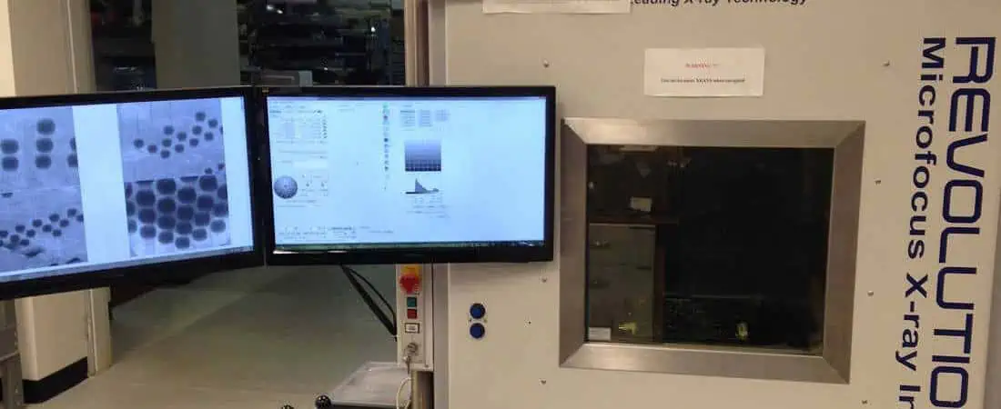
Key Components of an X-Ray Inspection System

  1. X-Ray Source: Generates the X-Ray radiation
  2. Detector: Captures the X-Rays after they pass through the object
  3. Image Processing Unit: Converts detected X-Rays into a visible image
  4. Display: Shows the processed image for analysis

Types of X-Ray Inspection Technologies

  1. 2D X-Ray Inspection: Provides a flat, two-dimensional image of the object
  2. 3D X-Ray Inspection: Creates a three-dimensional representation by combining multiple 2D images
  3. Computed Tomography (CT) Scanning: Generates detailed cross-sectional images of the object

Advantages of Using X-Ray Inspection for Quality Control and Safety

  • Non-destructive analysis
  • High-resolution imaging of internal structures
  • Rapid inspection of large quantities of products
  • Detection of defects invisible to the human eye
  • Consistent and objective results

Evolution of X-Ray Inspection Systems

From Medical Imaging to Industrial Innovation

X-Ray technology was first discovered in 1895 by Wilhelm Conrad Rรถntgen. Initially used for medical purposes, its potential for industrial applications was quickly recognized. Over the decades, X-Ray Inspection systems have undergone significant advancements, transforming various industries.

Advances in Technology

  • Digital Detectors: Replaced film-based systems, enabling real-time imaging and improved image quality
  • AI Integration: Automated defect detection and classification
  • Real-time Imaging: Allows for immediate analysis and decision-making
  • Increased Resolution: Enables detection of ever-smaller defects

Industry Adoption Trends

The adoption of X-Ray Inspection systems has seen exponential growth across industries. From electronics to food production, more sectors are recognizing the value of this technology for ensuring product quality and safety.

Read more about:

Industrial Applications of X-Ray Inspection Systems

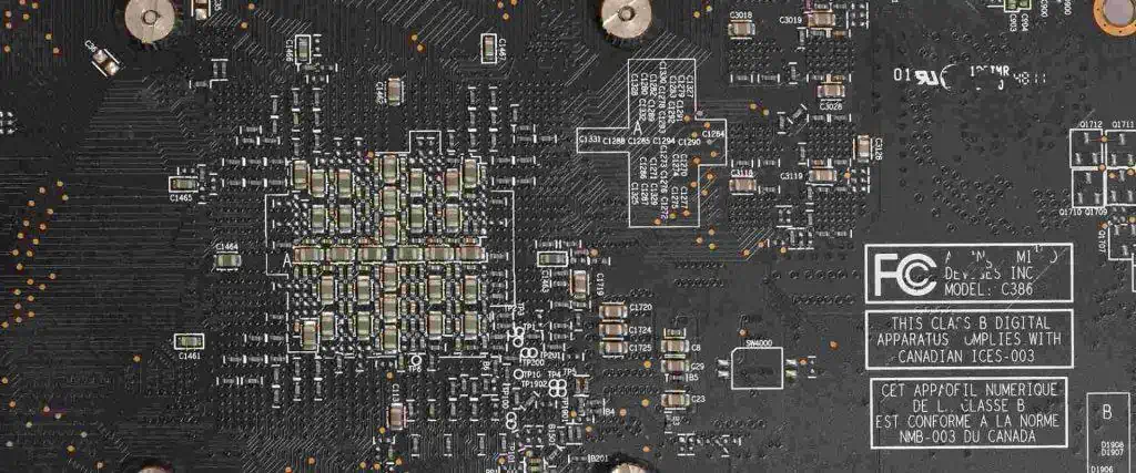
Electronics and Semiconductors

In the fast-paced world of electronics manufacturing, X-Ray Inspection systems play a crucial role in quality assurance.

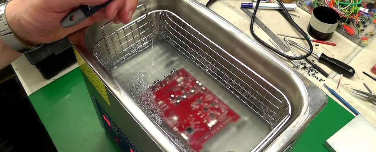
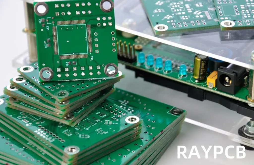
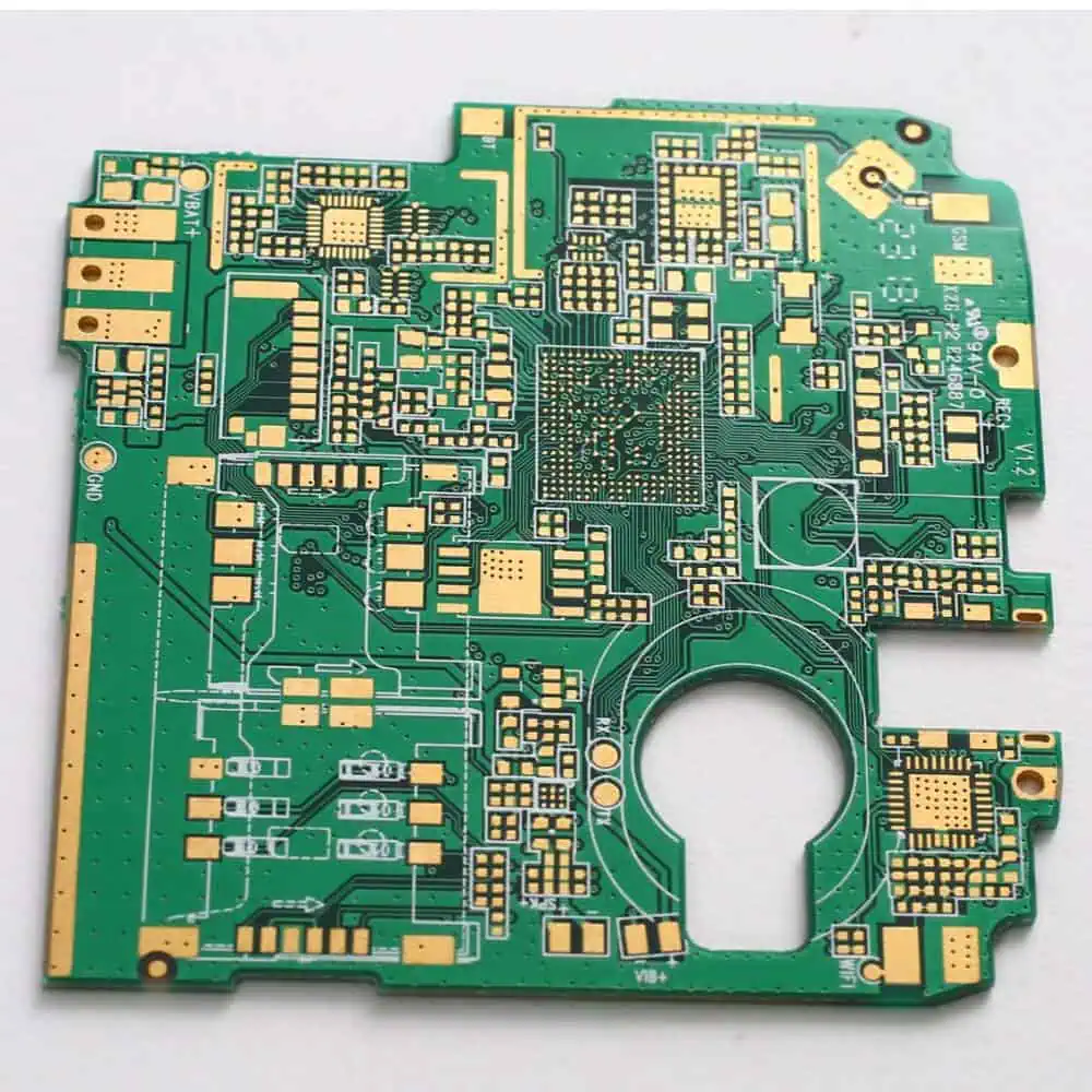
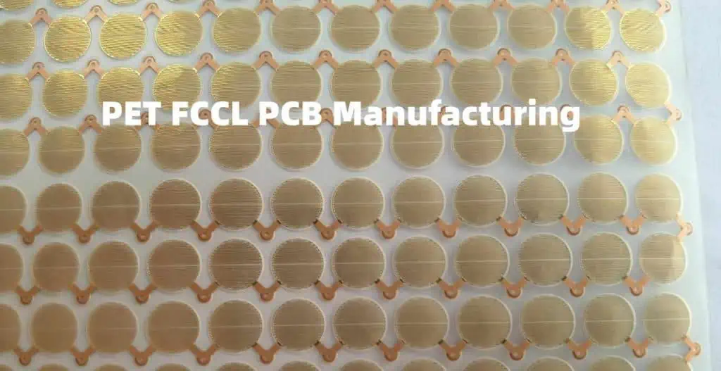
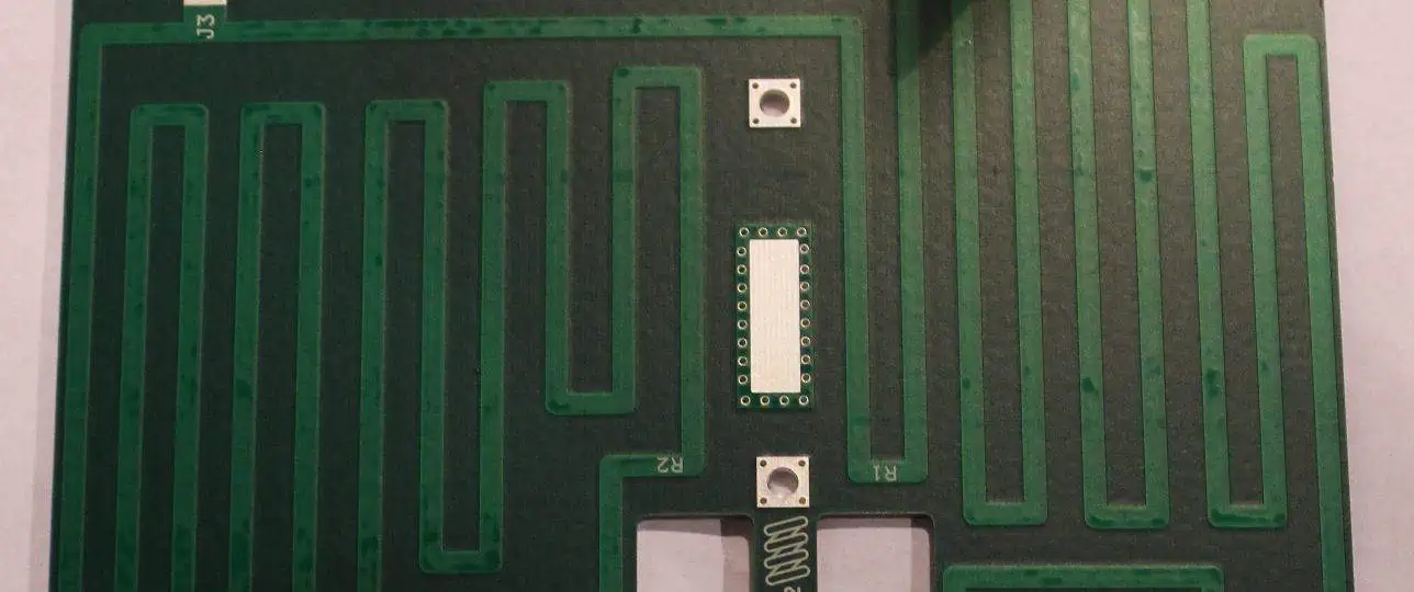
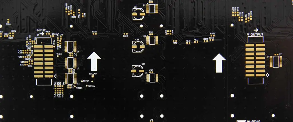
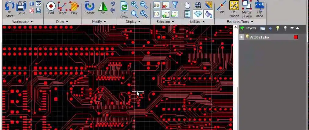
  • PCB (Printed Circuit Board) Inspection: X-Ray systems can detect hidden soldering defects, such as voids, bridges, and insufficient solder, which are invisible to optical inspection methods.
  • Semiconductor Package Inspection: X-Ray Inspection helps identify issues like wire bond integrity, die attach problems, and internal cracks in microchips.

Aerospace and Automotive Industries

Safety is paramount in aerospace and automotive manufacturing. X-Ray Inspection systems ensure the integrity of critical components without the need for disassembly.

  • Turbine Blade Inspection: Detects internal defects in turbine blades, crucial for aircraft engine safety.
  • Weld Inspection: Identifies flaws in welded joints, essential for structural integrity.
  • Composite Material Analysis: Examines the internal structure of lightweight composite materials used in modern vehicles and aircraft.

Food and Beverage Industry

X-Ray Inspection systems have become indispensable in ensuring food safety and quality.

  • Foreign Material Detection: Identifies contaminants like metal, glass, stone, or bone fragments in food products.
  • Package Inspection: Ensures proper fill levels and detects damaged or missing products in sealed packages.
  • Compliance with Food Safety Regulations: Helps manufacturers meet stringent safety standards and avoid costly recalls.

Pharmaceuticals

In the pharmaceutical industry, X-Ray Inspection systems are crucial for maintaining product quality and patient safety.

  • Packaging Integrity: Checks blister packs, vials, and other packaging for defects or contamination.
  • Dosage Verification: Ensures correct pill count and uniformity in medication packaging.
  • Contamination Detection: Identifies foreign particles in liquid medicines or powders.

Construction and Infrastructure

X-Ray Inspection plays a vital role in non-destructive testing (NDT) of buildings and infrastructure.

  • Concrete Inspection: Detects rebar placement, voids, and cracks in concrete structures.
  • Pipeline Inspection: Identifies corrosion, cracks, or other defects in underground pipes without excavation.
  • Bridge and Highway Inspection: Assesses the structural integrity of critical infrastructure components.

H2: Emerging and Specialized Applications

Art and Archaeology

X-Ray Inspection systems have opened new avenues in the study and preservation of art and historical artifacts.

  • Painting Analysis: Reveals underlying layers, artist’s techniques, and authenticity of artworks.
  • Artifact Examination: Allows non-invasive study of delicate archaeological finds and mummies.
  • Fossil Inspection: Helps paleontologists examine fossils embedded in rock without damaging the specimens.

Energy Sector

The energy industry relies on X-Ray Inspection for quality control and safety assurance.

  • Battery Inspection: Examines the internal structure of batteries for defects or inconsistencies.
  • Solar Panel Quality Control: Detects micro-cracks and other defects in solar cells.
  • Nuclear Fuel Rod Inspection: Ensures the integrity and safety of nuclear fuel assemblies.

Defense and Security

X-Ray Inspection systems are crucial for maintaining security in various settings.

  • Cargo Screening: Detects contraband or dangerous materials in shipping containers.
  • Luggage Inspection: Identifies potential threats in airport baggage.
  • Explosives Detection: Assists in the identification and safe handling of explosive devices.

Additive Manufacturing (3D Printing)

As 3D printing technology advances, X-Ray Inspection becomes increasingly important for quality assurance.

  • Internal Structure Verification: Ensures the integrity of complex internal geometries in 3D-printed parts.
  • Porosity Analysis: Detects voids or inconsistencies in printed materials.
  • Dimensional Accuracy: Verifies that printed parts meet design specifications.

Benefits of Using X-Ray Inspection Systems Across Industries

The widespread adoption of X-Ray Inspection systems across various industries is driven by several key benefits:

  1. Non-destructive and Non-invasive Testing: X-Ray Inspection allows for thorough examination without damaging the product or requiring disassembly.
  2. Early Defect Detection: By identifying issues early in the production process, manufacturers can prevent costly mistakes and improve overall quality.
  3. Quality Assurance: X-Ray Inspection provides consistent and objective results, ensuring that products meet stringent quality standards.
  4. Increased Safety: In industries like aerospace and automotive, X-Ray Inspection helps prevent catastrophic failures by detecting hidden flaws.
  5. Regulatory Compliance: Many industries use X-Ray Inspection to meet safety regulations and standards, particularly in food and pharmaceutical production.
  6. Reduction in Product Recalls: By catching defects before products reach the market, companies can significantly reduce the risk and cost of recalls.
  7. Liability Risk Mitigation: Thorough inspection processes help protect companies from potential lawsuits related to product defects.

Challenges and Considerations

While X-Ray Inspection systems offer numerous benefits, there are also challenges to consider:

Cost of Installation and Maintenance

X-Ray Inspection systems can represent a significant initial investment. Additionally, ongoing maintenance and potential upgrades add to the total cost of ownership.

H3: Need for Specialized Training

Operating X-Ray Inspection systems requires specialized knowledge. Companies must invest in training personnel to effectively use and interpret the results of these systems.

H3: Radiation Safety and Regulatory Compliance

The use of X-Ray technology necessitates strict adherence to safety protocols and regulations. This includes proper shielding, monitoring of radiation exposure, and compliance with local and international safety standards.

Future Trends in X-Ray Inspection

As technology continues to advance, several trends are shaping the future of X-Ray Inspection:

Integration of AI and Machine Learning

Artificial Intelligence and Machine Learning algorithms are being integrated into X-Ray Inspection systems, enabling:

  • Automated defect recognition and classification
  • Predictive maintenance of inspection equipment
  • Continuous improvement of inspection accuracy

Portable and Miniaturized X-Ray Inspection Systems

The development of smaller, more portable X-Ray systems is expanding the potential applications of this technology, allowing for:

  • On-site inspections in remote locations
  • Easier integration into production lines
  • More flexible and adaptable inspection processes

H3: Growing Role of 3D X-Ray and Computed Tomography (CT)

As 3D printing and complex manufacturing processes become more common, the demand for advanced 3D X-Ray and CT scanning is increasing. These technologies offer:

  • More detailed analysis of internal structures
  • Better visualization of complex geometries
  • Enhanced capability for reverse engineering and quality control

Conclusion

X-Ray Inspection systems have come a long way from their origins in medical imaging. Today, they play a crucial role in ensuring quality, safety, and efficiency across a wide range of industries. From electronics and aerospace to food production and art conservation, X-Ray Inspection technology is transforming how we approach quality control and non-destructive testing.

As industries continue to evolve and face new challenges, the versatility and capabilities of X-Ray Inspection systems make them an invaluable tool. The ongoing advancements in this technology, including AI integration, miniaturization, and improved 3D imaging, promise even greater applications in the future.

As X-Ray Inspection technology continues to evolve, its applications beyond medical imaging are only expected to expand further. This technology will undoubtedly play a pivotal role in shaping the future of quality assurance and safety across numerous industries.

Frequently Asked Questions

  1. What industries use X-Ray Inspection systems? X-Ray Inspection systems are used in various industries including electronics, aerospace, automotive, food and beverage, pharmaceuticals, construction, energy, defense, and even art and archaeology.
  2. Is X-Ray Inspection safe for food products? Yes, X-Ray Inspection is safe for food products. The radiation levels used are very low and do not affect the food’s taste, texture, or nutritional value.
  3. How does X-Ray Inspection differ from other inspection methods? X-Ray Inspection allows for non-destructive examination of internal structures, unlike visual or tactile inspection methods. It can detect defects and issues that are not visible from the outside.
  4. Can X-Ray Inspection systems detect all types of defects? While X-Ray Inspection is highly effective, it may not detect all types of defects. Its effectiveness depends on the material being inspected and the nature of the defect. It’s often used in combination with other inspection methods for comprehensive quality control.
  5. How are X-Ray Inspection systems becoming more environmentally friendly? Modern X-Ray Inspection systems are becoming more energy-efficient and use digital technologies that reduce the need for chemical processing of X-Ray films, making them more environmentally friendly than older systems.

How to clean a circuit board without alcohol?

No-Clean Flux vs. Water Soluble Flux

Circuit boards are crucial for the basic functioning of the majority of electronics and tech gadgets. Any defects in these circuit boards can lead to the complete failure of a device. Due to this reason, it is important to maintain and clean them from time to time to keep them from possible risks and problems. 

Over time, due to the frequent working of these circuit boards, these can gather debris and dirt that hampers their performance in the long run. Cleaning these circuit boards with alcohol is a common practice, but there are other alternatives available that can help you in this regard. We are going to discuss them in this post for you! Letโ€™s get started! 

Why Clean a Printed Circuit Board?

Some people often think about why cleaning a circuit board matters. There are many reasons for it. We need to maintain these circuit boards so that they can serve us longer. Plus, these can remain protected from possible dirt and debris as well. Thus regular cleaning of circuit boards saves a producerโ€™s time and reduces the chances of reworking as well. 

ยท       Improve the Aesthetic Appearance of the Printed Circuit Board

The overall appearance of PCBs matters a lot in this industry, and due to this reason, producers have to pay close attention to it. One way of making these PCBs is to clean them properly. Dirty and greasy PCBs are not aesthetic, and due to this reason, there are more chances of short circuits and poor performance in the long run. 

ยท       Enhance the Reliability of Printed Circuit Board

Clean and maintained PCBs are more reliable for sensitive and high-frequency devices. The measure of PCB cleaning is important for making them reliable to perform under pressure conditions easily. The reason is that due to the accumulation of dirt and debris, there are chances that PCBs can undergo short circuits and technical failures from time to time. 

ยท       Control Printed Circuit Board Component Corrosion

The best part about PCB cleaning is that we can save sensitive PCB parts from rusting and corrosion over time. Proper cleaning can easily prevent this problem and removes the moisture from these parts that initiate corrosion. 

ยท       Avert Adhesion Issues 

Problems occur when we cannot handle the flux on PCBs properly. Due to this reason, adhesion can occur, and it can ruin the conformal coating and sensitive PCB layers at the same time. It means we can solve the adhesion problem by cleaning PCBs. 

ยท       Evade Dendritic Growth 

Sometimes workers can leave out the flux remains that are ionic particles. After some time, these can interact with moisture and can develop dendrites when the current is passing. This results in poor performance of PCBs for the electronics. The dendritic chain formed in this way can be a major cause of current leaks and other technical complications.ย 

What are the causes of Printed Circuit Board corrosion?

Clean a Printed Circuit Board

There might be electronic devices that do not come with circuit boards. These are highly significant in the fine performance of devices as well. When we frequently use our electronic devices, there are chances that, with time, they can undergo complete failure due to the accumulation of dirt and debris, leading to holding back our devices to perform smoothly. In some cases, the presence of moisture in the circuit boards can make them undergo corrosion as well.  

Why Avoid Alcohol for Printed Circuit Board Cleaning?

There is no doubt that using alcohol for circuit board cleaning is a common practice, but there are some concerns the experts have regarding it. Alcohol is good for intensive cleaning of circuit boards fastly, but some circuit boards are too sensitive to tolerate the impact of alcohol on them. Using alcohol on such circuit boards can erode their structure, and the metal on them might strip off as well. 

Essential Precautions Before Cleaning

Below you will find some effective safety tips that you have to consider while cleaning circuit boards by following any type of cleaning method: 

  1. Power Off and Unplug: Make sure to turn off/power off the electronic device that you want to clean and plug it out from the power source. 
  2. Antistatic Measures: Always make use of antistatic measures like weaning an antistatic wrist strap and using a mat to ensure quick discharging of static entities on the whole. 
  3. Visual Inspection: It is better to visually check the circuit board before cleaning and see if there are any broken traces and damaged components or not. Since any type of cleaning agent can easily do more damage to these damaged components of the circuit board. 
  4. Isopropyl Alcohol Concentration: Alway uses alcohol with 70% or less concentration since it won’t be harmful to the sensitive circuit boards. 

Methods to clean a circuit board without alcohol

PCB Cleaning
PCB Cleaning

Now we are going to see the alternative methods that we can opt for cleaning circuit boards other than alcohol. Letโ€™s check them out below: 

Method 1: Compressed Air

Compressed air is important when we want to reach the congested areas and remove the dust and debris tightly stuck in these restricted areas of the circuit boards: 

  • Hold the compressed air device and make sure to use small blows for cleaning the circuit board since harsh blowing can damage the components.
  • Make sure to blow the circuit board from some angles where you see excessive debris and dirt that needs immediate removal. 
  • Take care of the compressed air can as well since problems can occur if you want to make full use of this device in the long run. 

Method 2: Soft Brush and Cotton Swabs

You can even rely on a soft brush and cotton swabs for complete cleaning of circuit boards. These are fragile, and you can reach out to sensitive circuit board components through these tools quite easily. 

1.      Brush Cleaning: A brush with soft bristles can easily clean the circuit board without compromising the circuit parts. 

2.      Cotton Swabs: Immerse the cotton swabs with distilled water and then use them on the circuit board. 

3.      Spot Cleaning: Make sure to follow the spot cleaning approach that ensures complete debris removal from a circuit board.

Method 3: DIY Cleaning Solution

Another method is to use a DIY cleaning solution that you can easily make it home for the circuit board cleaning. 

1. Take a little amount of distilled water and mix it with a less-invasive cleaning detergent. 

2. Now, take a damp cloth and do not make it too wet since it can cause problems. 

3. Do gentle strokes and carefully clean the sensitive circuit board parts. 

4. Now dry the circuit board with a dry soft towel. 

Method 4: Baking Soda Paste

Baking soda is effective for intense and rigorous circuit board cleaning. Due to this reason, we have to be extra careful with it to drive positive results. 

1. Make a paste of baking soda & distilled water. 

2. Take a soft brush or a cotton swab and dit it in the mixture. 

3. Rub it on the dirty and greasy areas with utmost care. 

4. Use a dry cloth to remove any moisture left on the surface of the board. 

Method 5: Distilled Water Rinse

We can even use distilled water for solo rinsing of the circuit boards, and this is one of the easiest methods of cleaning circuit boards without alcohol. 

1. Use a soft cloth and dip it in the distilled water for cleaning. 

2. Remove any grease, residues, and debris on the surface with this cloth. 

3. Don’t forget to dry the circuit board using a dry cloth. 

4. Give the circuit board a compressed air blow to make sure that there is no moisture left in the setup. 

Method 6: White Vinegar Solution

Diluted vinegar is also good for removing the chemical stains left on the circuit boards. Letโ€™s see how we can use it effectively. 

1. Use diluted vinegar and distilled water to make a mixture. 

2. Use soft brushes and dip them in the mixture to use them for cleaning. 

3. Now clean the stains with the help of these brushes. 

4. Dry out the circuit board carefully to remove all the moisture. 

Tips for Safe Printed Circuit Board Cleaning

  • Never rely on invasive chemicals and intense cleaning agents for cleaning the circuit boards. 
  • Make sure to clean the circuit board in an open area that allows seamless ventilation.
  • Try to cover your face and eyes while cleaning the circuit boards to prevent any sort of skin and eye infection.
  • Wear protective cleaning equipment while cleaning the circuit boards. 
  • First, make sure to dry the circuit board before plugging your device back in. 
  • In any confusion, seek professional help from the experts. 

Conclusion

Cleaning circuit boards matter a lot for the performance of electronics. In this post, we have described effective methods that you can perform if you are unable to use alcohol for this purpose. From now on, you can easily maintain your circuit boards from dirt, debris, and possible damage from corrosion on all counts!

Inexpensive PCB Prototyping: Compare Prices & Save on Your Next Project

PCB prototype assembly suppliers

In today’s fast-paced world of electronics, printed circuit boards (PCBs) are the backbone of nearly every electronic device. Whether you’re a hobbyist, a startup, or an established company, understanding and managing PCB prototype costs is crucial for successful project development. This comprehensive guide will walk you through everything you need to know about PCB prototyping costs, helping you make informed decisions and save money on your next project.

Understanding PCB Prototype Costs

Before diving into cost-saving strategies, it’s essential to understand what factors influence PCB prototype costs. By grasping these elements, you’ll be better equipped to make cost-effective decisions without compromising quality.

Factors Affecting PCB Prototype Cost

  1. Board Size: The physical dimensions of your PCB directly impact the cost. Larger boards require more materials and processing time, increasing the overall expense.
  2. Layer Count: Single-layer boards are the most economical, while multi-layer boards increase in cost with each additional layer. Complex designs often require multiple layers, balancing functionality with cost.
  3. Material Selection: The choice of substrate material affects both performance and price. FR-4 is a common, cost-effective option, while specialized materials like Rogers or polyimide can significantly increase costs.
  4. Copper Weight: Thicker copper layers are more expensive but may be necessary for high-current applications or improved heat dissipation.
  5. Surface Finish: Different finishes like HASL, ENIG, or immersion gold offer varying levels of protection and solderability at different price points.
  6. Minimum Trace Width and Spacing: Tighter tolerances require more advanced manufacturing processes, increasing costs.
  7. Drill Hole Density: More holes per square inch require more time and specialized equipment, driving up the price.
  8. Quantity: Economies of scale apply to PCB production. Ordering larger quantities can reduce the per-unit cost, but may not always be practical for prototyping.
  9. Turnaround Time: Expedited services come at a premium. Standard production times are more economical but require patience.

Strategies for Reducing PCB Prototype Costs

Now that we understand the factors influencing PCB prototype costs, let’s explore strategies to minimize expenses without sacrificing quality or functionality.

1. Optimize Your Design

Efficient design is the foundation of cost-effective PCB prototyping. Consider the following tips:

  • Minimize Board Size: Compact designs not only save on material costs but can also improve electrical performance.
  • Reduce Layer Count: Challenge yourself to accomplish your design goals with fewer layers when possible.
  • Standardize Components: Using common, readily available components can reduce overall costs and improve manufacturability.

2. Choose Materials Wisely

While high-performance materials have their place, they’re not always necessary for prototyping. Consider these material choices:

  • Stick with FR-4: For most prototypes, standard FR-4 is sufficient and cost-effective.
  • Evaluate Copper Weight: 1 oz copper is adequate for many applications and is less expensive than thicker options.
  • Select Economical Surface Finishes: HASL (Hot Air Solder Leveling) is often the most budget-friendly option for prototypes.

3. Leverage Design for Manufacturing (DFM) Principles

Adhering to DFM guidelines can significantly reduce manufacturing costs and improve yield:

  • Use Standard Drill Sizes: Avoid specifying odd-sized holes that require special drill bits.
  • Maintain Reasonable Trace Widths: Wider traces are easier and cheaper to manufacture than extremely thin ones.
  • Consider Panelization: For smaller boards, panelizing multiple designs can reduce costs.

4. Explore Different Manufacturers

PCB prototype costs can vary significantly between manufacturers. Consider the following when choosing a supplier:

  • Compare Quotes: Get quotes from multiple manufacturers to find the best balance of cost, quality, and service.
  • Look for Bundled Services: Some manufacturers offer design review, assembly, and testing services that can be more cost-effective than using separate vendors.
  • Consider Overseas Options: While domestic manufacturers may offer faster turnaround times, overseas suppliers often provide lower costs for those with flexible timelines.

5. Optimize Order Quantities

Finding the sweet spot in order quantity can lead to significant savings:

  • Evaluate Minimum Order Quantities: Some manufacturers offer better rates for slightly larger orders. Calculate if ordering a few extra boards could reduce your per-unit cost.
  • Plan for Future Iterations: Consider ordering extra boards to account for potential design revisions, which can be more cost-effective than placing multiple small orders.

Read more about:

Advanced Techniques for PCB Prototype Cost Reduction

For those looking to further optimize their PCB prototype costs, consider these advanced strategies:

1. Embrace Open-Source Tools

Utilizing open-source PCB design software can significantly reduce upfront costs:

  • KiCad: A powerful, free PCB design suite that rivals many commercial offerings.
  • FreePCB: Another free option suitable for simpler designs.
  • Eagle (Free Version): While limited in board size and layers, it’s sufficient for many prototype projects.

2. Participate in Group Orders

Some online communities and PCB manufacturers offer group ordering services:

  • PCB Prototyping Services: Platforms like PCBWay and JLCPCB sometimes offer group buy options.
  • Maker Communities: Join maker spaces or online forums where members sometimes organize group PCB orders.

3. Consider Flex PCB Alternatives

For certain applications, flexible PCBs might be a cost-effective alternative:

  • Reduced Assembly Costs: Flex PCBs can eliminate the need for connectors and wiring in some designs.
  • Space Savings: In compact designs, flex PCBs can reduce overall product size and complexity.

4. Leverage Additive Manufacturing

For extremely low volume or highly iterative prototyping, consider additive manufacturing techniques:

  • 3D Printed Electronics: While not suitable for all applications, 3D printed circuits can be incredibly cost-effective for certain prototypes.
  • Conductive Ink Printing: Another emerging technology that can be useful for quick, low-cost prototyping of simple circuits.

Balancing Cost and Quality in PCB Prototyping

Rogers RO4500 PCB

While reducing PCB prototype costs is important, it’s crucial to maintain a balance between cost-saving measures and the quality required for your project. Here are some considerations:

1. Identify Critical Components

Not all parts of your PCB design require the same level of precision or quality:

  • High-Speed Sections: Areas with high-frequency signals may require better materials or tighter tolerances.
  • Power Distribution: Sections handling high currents might need thicker copper or special considerations.
  • Standard Interfaces: Areas with standard connectors or low-speed signals can often use more economical manufacturing options.

2. Invest in Design Verification

Spending a bit more on design verification can save significant costs in the long run:

  • Simulation Software: Tools like SPICE can help identify potential issues before manufacturing.
  • DFM Checks: Many PCB design software packages include DFM checks that can catch costly errors early.
  • Professional Review: For critical projects, investing in a professional design review can be well worth the cost.

3. Consider the Entire Product Lifecycle

When evaluating PCB prototype costs, consider the entire product development cycle:

  • Iterative Prototyping: Sometimes, investing in multiple, less expensive prototype runs can be more cost-effective than trying to perfect the design in one expensive iteration.
  • Scalability: Ensure your prototype design can be easily scaled for production without requiring major changes.
  • Long-term Reliability: Cutting costs on critical components or processes might lead to reliability issues that are more expensive to fix later.

Conclusion: Mastering PCB Prototype Costs

Successfully managing PCB prototype costs requires a multifaceted approach. By understanding the factors that influence costs, implementing smart design strategies, and leveraging cost-saving techniques, you can significantly reduce your PCB prototyping expenses without compromising on quality or functionality.

Remember, the goal of prototyping is to validate your design and identify potential issues early in the development process. While cost is an important factor, it shouldn’t come at the expense of achieving these primary objectives.

By applying the strategies and insights shared in this guide, you’ll be well-equipped to navigate the world of PCB prototyping, making informed decisions that balance cost, quality, and performance. Whether you’re working on a hobby project, a startup innovation, or a corporate product development initiative, mastering PCB prototype costs will give you a competitive edge and help bring your electronic designs to life more efficiently and economically.

As you embark on your next PCB prototyping project, remember that each design presents unique challenges and opportunities for cost optimization. Stay curious, keep learning, and don’t hesitate to experiment with different approaches. With persistence and smart decision-making, you’ll find the perfect balance between cost-effectiveness and performance for your PCB prototypes.

What is Corne PCB?

Corne PCB

Corne keyboard is a type of spilt keyboard with support for the ortho split keyboard structure. Designed by Foostan, it has become one of the best keyboards for people looking for a unique typing experience. With the RGB lighting, you can be sure of maximizing the keyboard for the best results.

In this blog post, we introduce you to what the Corne keyboard PCB is and the different variations you can find it.

Does the Corne Keyboard Need a PCB?

A Printed Circuit Board (PCB) is used to harmonize the performances of electronic components, especially by grouping them into one house.

With the Corne keyboards, the PCB has a special use โ€“ coordinating the interconnections of the components. You will find the circuit board handy when working with a Corne kit.

What is a Corne Kit?

The flexibility of the Corne keyboards allows you to assemble or couple new keyboards, depending on what you want them for.

In this case, you may not be going for the Corne keyboard prebuilt, but looking to build a custom variant. You need a Corne kit for this purpose โ€“ a set of components that make the custom keyboard development easier.

The Types of Corne Kits

Corne PCB Layout
Corne PCB Layout

There are different kinds of kits you can buy and use for assembling the Corne keyboards. It all depends on where you are buying from.

In this section, we outline some of the popular Corne kits you can use.

1.    Corne Cherry Kit

This is from the stables of KeebMaker. The Corne Cherry Kit is a โ€œsplit, columnar keyboard with a super small footprint.โ€

Kit Variations

You will find variants of the Corne Cherry Kit. You can use either of them for building custom keyboards.

The first variant is the 36-key kit, which supports the breakaway of the outer columns of the Corne keyboards. You will receive the v.2.1. Printed Circuit Boards (PCBs) alongside this kit.

The second variant is the 42-key kit, which provides you with the Corne V2 PCBs. These circuit boards also support the easier-to-solder SK6812 Mini-E LEDs.

Components of the Corne Cherry Kit

If you are buying this kit, irrespective of the variants, you will find included, a couple of base components. Examples are:

  • 2 TRSS Jacks
  • 2 Corne PCBS
  • 2 Reset Switches
  • Kailh Hotswap Sockets. You will receive the corresponding sockets depending on whether you are looking to build the Corne keyboards based on the V2.1. PCBs or the Corne V3 PCBs.
  • 2 USB-C Micro-controllers with square post headers and;
  • Diodes. You will get either that of 36 or 42, depending on the configuration of the PCB used.

Features of the Corne Cherry Kit

Besides offering two configuration options, as per the type of PCBs supported, the Corne Cherry Kit also has some impressive features. These include:

a.     Dual OLED Screens

The Corne keyboard kit supports the making of OLED screens on both halves. The screens are fully-programmable and support different kinds of displays, such as:

  • WPM graphs
  • Cute animations and;
  • Diagnostic charts
b.    MX Profile Support

The keyboards made out of the kit support all the MX profile key switches. Besides, the flexibility allows you to use custom key switches for this purpose, even if you donโ€™t source them from KeebMaster.

c.     Support for Breakaway Outer Columns

One of the major benefits of split keyboards is the two-piece design that improves typing speed and keeps the forearms, hands and wrists at a comfortable width.

Based on this, the Corne Cherry Kit supports the breakoff or breakaway of the PCBsโ€™ outer columns. This enables the further reduction of the keys from 42 to 36.

d.    Full RGB Lighting

The kit contains the easy-to-solder KeebMaker Corne SK6812 Mini-E LEDs for the per-key lighting.

Full RGB lighting is also provided via the placement of RGB lighting beneath the keyboard and under each of the keys.

2.    Aurora Corne PCB Kit

This is another type of PB kit you can use for the Corne keyboard. The kit is compatible with the following:

  • Choc/MX Hand Solder
  • MX Hotswap and;
  • Choc Hotswap

Design Specifications

It is worth point pointing out that the Aurora Corne PCB Kit is a redesign of the original keyboard by Foostan.

It is portable, and comes with a โ€œrelatively small split keyboard with 42 keys.โ€

Kitโ€™s Variants

You will find the kit available in 3 variants โ€“ Choc Hotswap, Choc/MX Hand Solder and MX Hotswap.

A special focus is on the hotswap kit, which comes with 42 pieces of the Hotswap socket in either MX or Choc.

The Choc Hotswap kit specifically, comes with additional properties, such as:

  • SMD resistors, which are used in place of the axial ones.
  • SMD diodes

Features of the Aurora Corne PCB Kit

This kit provides you with a lot of unique features, such as support for both tenting puck and a power switch for the wireless controllers. This comes in handy when making a Corne wireless PCB keyboard.

The kit also supports MX spacing for all the variants, up to two 128×32 pixel OLED displays, a compact layout featuring 42 keys; and is powered by either the ZMK or QMK firmware.

How to Build a โ€œWorking Corne Keyboardโ€

Corne keyboard PCB
Corne keyboard PCB

With the features and the inclusion of important components like 2 reset buttons, a left and a right PCB, as well as 5 pieces of the 4k7 Ohm axial resistors; you are almost on the way to build a custom Corne PCB keyboard.

However, to make the keyboard work as expected, you would need a couple of other components. These include:

  • 1 x TRRS cable
  • 2 pieces of the Pro Micro-compatible controllers
  • 42 x Kalih Choc or MX-compatible keycap
  • 42 x Kalih Choc or MX-compatible switch and;
  • 1 x USB cable that is compatible with the selected controller. You can choose between the Micro USB to USB A and USB-C.

You may also want to get additional components, such as a set of Corne keyboard cases required for protecting the keyboards during transport and when in use.

Conclusion

The popular Corne keyboard, also called the Helidox or crkbd was created by Foostan and has become a model for new keyboard kits. As an open-source keyboard kit, it paved the way for new kits to be produced and which would be used to enhance the production of more split keyboards based on the original Corne concept.

Flexible Copper PCB: What Makes this Circuit Board Bendable?

Flexible Copper PCB Laminate

Have you ever heard that a circuit board is โ€œbendable?โ€ Yes, it is possible for a circuit board to bend and the name for it is flexible copper PCB.

In case this is your first time of hearing the term, this article is a pointer to the right direction. You will find out the meaning of flexible copper circuit board, as well as some of the properties.

What is Flexible Copper PCB?

As the name suggests, it is a type of Printed Circuit Board (PCB) that is flexible, i.e., can be bent or turned into different forms โ€“ for different purposes.

Understanding the Structure of Flexible Copper PCB

fpc-flexible-printed-circuit

The first step to understanding how a flexible circuit board works is by taking note of the structure.

One unique feature is that it takes a similar pattern or shape to the rigid Printed Circuit Board (PCB), in the sense that the board has a good dielectric material and higher temperature resistances.

With that being said, here is a breakdown of all that go into the structure of the flexible copper circuit board.

a.    The Dielectric Substrate Film

This is the first thing you will notice about the flexible copper PCB. The board uses a layer of Polyimide (Pi), which serves as the base material. The material is also characterized by high resistance to both the temperature and traction.

b.    Electrical Conductors

This is where the โ€œcopperโ€ in flexible copper PCB is derived from. The electrical conductors refer to the copper, which represents and is used for routing the traces of the circuit board.

c.    The Coating/Protective Finish

This is the โ€œprotective featureโ€ used to prevent a contamination of the copper in particular and the PCB in general.

The protective finish is commonly made of cover coat.

d.    The Adhesive Material

Next on the list is the adhesive material, which is the material required for making the โ€œboard stick.โ€

The adhesive layer of epoxy resin is commonly used but you can also substitute with polyethylene. The goal of the adhesive material is to join the several parts of the flexible copper PCB, especially the bonding of the copper foil layer on the top layer.

The above is the function of the adhesive material on the single-sided flexible PCB. For the double-sided or multilayered version of the circuit board, you can use the adhesive material to join the upper and bottom layers of the copper foil.

The Classifications of Flexible Copper PCB

You can find different types of flexible circuit boards in the market. While the single-sided variant is the one you can commonly interact with, it has other variants.

There is the double-sided flexible board, which, as the name suggests, has two sides.

Then, there is the multi-sided or multilayered flexible copper board, which uses more than 2 layers or sides.

The Fabrication Processes of Flexible Copper PCBs

Note that the process of fabricating or manufacturing the flexible circuits differ, by the number of sides or layers. For example, you will find the process of the single-sided variant different and possibly, easier than that of the double-sided or the multilayered.

a.    Fabricating a Single-Sided Flexible Circuit Board

The flexible board using a single side is fabricated, first, by making a slit cut of the roll-shaped Polyimide copper flexible base material into the size of the flexible PCB, as specified by the customer(s).

The next steps include the development and transfer of the circuit to the copper foil. The process of exposure etching is used for the purpose and while the etching part of the PCB is retained, the other (residual) parts are taken off.

The required holes are made on the PCB, before E-testers will be used to validate the circuit boardโ€™s performance.

Subsequent steps to take include:

  • Pasting a Polyimide protective film on the copper layer to protect it from oxidation and contamination;
  • Lamination;
  • Apply the solder mask and legends;
  • Using curing bake to cure the solder mask and legends;
  • Implementing the surface treatments, such as Immersion Gold, OSP, and LF-HASL;
  • Doing a second test to confirm that the circuit board is of high-quality;
  • Fixing-up the boardโ€™s appearance, before packaging it.
  • The last round of inspections is made to validate the package before it is shipped.

b.    Fabricating Double-Sided and Multilayered Flexible Copper PCBs

The processes of manufacturing double-sided and multi-sided flexible circuit boards are similar to those of the single-sided variants โ€“ but with a few additions.

For example, as soon as the base material is transferred to the flexible PCB size, the first drilling should be done. This is to be followed by the electroplating the copper foil โ€“ and then, the plating of the vias with copper.

The circuit design will be transferred to the copper foil via exposure, and etching process takes place โ€“ removing the residual parts and retaining the etching part.

The fabrication continues with the punching of holes on the PCB, running the first round of inspections with E-testers and doing the cleaning and grinding of the board.

The protection of the PCB is done with the pasting of the Polyimide protective film, application of the solder mask and legends; curing of the legends and the solder mask; and the implementation of surface treatment as a way of preventing pad oxidation.

Just like the single-sided flexible copper PCB, the next processes include:

  • Running a second round of test/inspection to confirm that the circuit board is in good working condition.
  • Using a knife mold to cut-off the size, as specified by the customer(s).
  • Taking note of the physical appearance of the board and fixing any design flaws at this stage.
  • Packaging the double/multi-sided flexible copper PCBs and having random inspections to ensure the consistency of the number of labels, boxes and marks before shipping.

Final Words

Flexible copper circuit boards are popular because of the reliability, freedom it grants the designer to mold it into different shapes and for different purposes. These boards also have higher temperature resistances (especially between -200หšC and 400หšC) โ€“ and they can help reduce the incidences of human errors during wiring.

FCCL PCB: What is Flexible Copper Clad Laminate?

FCCL PCB

In the making of Printed Circuit Boards (PCBs), some materials are outstanding. For the flexible circuits, the use of Flexible Copper Clad Laminate (FCCL) has become a trend. In this article, you will learn about what the FCCL PCB means.

The Background

Flexible Copper Clad Laminate or FCCL PCB is a sub-section of the broader Copper Clad Laminate (CCL). It is categorized based on the mechanical rigidity of the CCL.

The FCCL is one of the two circuit board laminates categorized based on the mechanical rigidity. The other is the Rigid Copper Clad Laminate (RCCL).

What is Flexible Copper Clad Laminate?

This is the base or core laminate/component of the Flexible Printed Circuit Board (FPCB). As the key or main material, it plays an important role in the functions of the circuit board.

It is also worth noting here that the FCCL features the layers of Polyimide and copper foil, which, in turn, are used as an insulator and electrical conductor for the board.

How Does the Copper Clad Laminate Stack-Up?

The composition of this material includes the lamination of copper foil onto the Polyimide Film (PI).

Also, the laminate comprises both the Thin Copper Foil and Polyimide Film (PI). While the film acts as the insulating substrate material, the thin copper foil is used as an electrical conductor on the surface.

The Broad Classifications of FCCL PCBs

The Flexible Copper Clad Laminate (FCCL) can be broadly grouped into:

  • Single-sided
  • Double-sided and;
  • Multi-sided FCCL PCBs

Now, these classifications are based on the number of sides that the board has โ€“ and the trace density. For the single-sided, it means that the circuit board has only the copper foil on one side, while the double-sided means the inclusion of copper foil on both sides. For the multi-sided boards, we are looking at the ones with copper foil on more than two (2) sides.

The Classifications Based on the Structures

The Flexible Copper Clad Laminate (FCCL) PCB can be further classified, grouped or divided into other sub-categories, based on the structures of the product. In this case, the major divisions are based on whether the circuit board uses adhesive or not.

Also, the consideration is whether adhesive is added in-between the copper foil(s) and Polyimide Film (PI). Irrespective of the presence of adhesive or not, the FCCL can still be used to fabricate the flexible PCBs.

The adhesive Flexible Copper Clad Laminate is also called 3L-FCCL, while the non-adhesive or โ€œadhesivelessโ€ is called the 2L-FCCL.

Differentiating between the Adhesive and Non-Adhesive FCCL

The major differences between the two is that the adhesive FCCL features adhesive in-between the Polyimide Film (PI) and the copper, while the non-adhesive doesnโ€™t.

Another difference between the two is that the non-adhesive Flexible Copper Clad Laminate (FCCL) costs more than the FCCL using adhesive.

In terms of the production capabilities and or applications, you can also differentiate between the two. On the one hand, the adhesive FCCL is ideal for manufacturing the following kinds of flexible circuit boards:

  • Simple flexible boards
  • Double-sided flexible circuit boards and;
  • Single-sided flexible circuit boards.

On the other hand, the non-adhesive FCCL is ideal for manufacturing the following types of flexible boards:

  • High-density SMDs, especially the ones with overlay openings.
  • Multilayer circuit boards
  • Rigid-flexible circuit boards
  • Impedance-controlled circuit boards and;
  • High-Density Interconnect (HDI) PCBs.

What You Need to Know About FCCL PCBs

Before choosing to work with this material or laminate, take note of the following points:

a.    The Need for Desired Thickness

There is a need to attain both the desired thickness and controlled impedance. For this reason, there may be a need to combine the different thicknesses of the following:

  • Coverlay
  • Flexible Copper Clad Laminate (FCCL)
  • Adhesive

Note that the combination is commonly required for special applications/uses.

b.    The FCCL Copper Pour Design

The term, โ€œcopper pourโ€ means the cross-hatched or solid area on a bare PCB, and this area must be filled with copper.

The functions of copper pour include:

  • Reducing the number of etching materials required for producing circuit boards.
  • Being used to make connections on the circuit boards and;
  • Improving the flexible bending capability of the Flexible Printed Circuit Board (FPBC).

There are different kinds of copper pour, such as cross-hatching/cross-hatched copper, hatching pour and solid copper pour.

Differences between the Copper Pours

While the functions of these pours border on improving the circuit boardsโ€™ bendability, reducing the etching materials used and improving connections โ€“ they also differ individually.

Here is how they compare:

Solid Copper Pours

It has become common practice for circuit board designers to use the solid areas of copper pour as the ground layers that cover the remaining areas outside the stand-off regions, the traces and the pads.

The solid copper pour can also be used to provide better resistive characteristics for the circuit board.

Hatched Copper Pour

The hatched copper pour has its role to play in the FCCL PCB. Among many other functions, it supports the adjustment of the impedance of high-frequency traces. This comes in handy for the improvement of the impedance capabilities.

Cross-Hatched Copper Pour

This type of copper pour is used to make a balance the dilatation and heat on both sides of the Printed Circuit Board (PCB). This goes a long way to avoid warping of certain PCB substrate(s).

c.    The Bending Capabilities

One of the unique attributes of the Flexible Copper Clad Laminate (FCCL) is the improved bending it offers. This is because of the base or primary material comprising the lamination of copper foil onto Polyimide Film (PI). This supports the realization of the ideal product design, with a special concentration on the sliding, bending and folding attributes.

Despite improving the bendability and foldability of the Flexible PCBs, the FCCL might have some discrepancies. An example is the thickness of the FCCL, whereby if one is adhesive and the other is not, then, the flexibility and bending of the non-adhesive FCCL becomes more prominent than that of the adhesive FCCL.

Wrapping Up

Flexible Copper Clad Laminate (FCCL) helps to bolster the flexible bending of the flexible circuit boards. For the best results, use only the adhesive or the non-adhesive, as using the two makes the non-adhesive more prominent.

Nevertheless, you can do without any of the two and the FCCL can still be used to fabricate and manufacture flexible Printed Circuit Boards (PCBs).

How to remove gold from circuit boards?

how to remove gold from circuit boards

If you are into circuit boards, then you already know that we include some fine metals like steel, iron, and gold in their structure for different purposes. We are not going to dig deeper into their purposes since we will be off-topic. Instead, in this post, we are going to see some of the easiest and most effective methods for gold removal from sensitive circuit boards.

Make sure to stick to the tips given in this guide so that you can have a better understanding of performing this in the time of need without relying on external help and expensive tools.

So letโ€™s see how it’s done!ย 

How to remove gold from circuit boards?

Remove gold from PCB

1.     Be Careful 

When we need to remove gold from the circuit boards, it is better to become highly choosy for chemical selection. There are some considerations to follow while doing this. For example, carefully storing the chemicals and revising protective ways to handle them to avoid compromising the environment at all. If you are using cyanide, then it is better to not only check its shelf life but also wear protective wearables while working with it since it is a highly dangerous chemical for usage. 

2.     Prepare Materials & Safety Equipment

The next thing that we need to do is to keep our materials and safety tools ready at hand. This type of gear comes in handy when you are handling hazardous materials and want to protect yourself from them as well. Take masks, goggles, protective suits, and gloves, for example. All of these serve the purpose of complete protection of workers when they interact with harmful chemicals and acids for gold removal.

3.     Follow Safe Handling Instructions

It is better to always stick to safe handling procedures, and these always come in handy to prevent mishaps and emergencies during work. There is no doubt that personal protective equipment is crucial, but there are some other protective measures that are important to consider to ensure complete safety. For example, covering your eyes, face, and body parts while working with chemicals and acids. Ensuring proper air ventilation where you are dealing with chemicals and gold removal from circuit boards. Once you are done, then wash your hands with cleaning agents and use sanitizers before eating or shaking hands with someone. Other than this, there is still a chance of seeking professional help from experts to avoid mishaps on all counts. 

4.     Prepare Electronics for Gold Extraction

The next step is to prepare your electronics that need gold removal. It is better to detach the components of these devices and divide them into three categories of plastic, metal, and glass. You can even isolate flammable materials during this process and carefully dispose of them to avoid any sort of complications. 

5.     Clean Off PCBs

Now we need to start the cleaning and see if there are any fragments of plastic, glass, and metal on the PCBs or not. There are some residues that we can take out with our hands, while others need specialized equipment. Acetone comes in handy for this purpose. It easily melts down stubborn metal shards on the circuit boards. However, while using acetone, you need to be cautious with its handling and protect your skin and sensitive circuit board components from it as well. 

6.     Create The Etching Solution

At this point, we need to use the etching solution that assists in complete gold removal from the circuit boards. We can even use a cyanide and water mixture for this purpose, but it is better to wear a protective suit and cover yourself properly while doing it. The amount of gold removed from the circuit board depends on the concentration of cyanide that we use in this mixture. In case when we are using high cyanide concentration, we need to handle it with extra care to avoid problems. 

7.     Extract the Gold Foils

Here comes the step when we perform gould foil extraction. Before we do this, it is important to dip the PCBs in the etching solution and take them out after waiting for a while. By relying on a metal brush, we can easily remove the gold from the circuit boards. All of this happens under professional supervision and without wearing protecting suits and using protective equipment; experts don’t recommend performing this step at all. 

8.     Filter Out Gold Foils

The next step is to filter the gold foils after removing them from the circuit boards. We can filter them by using the same etching solution. The better way is to pour the solution into a plastic glass or container. It immerses the foils in the bottom of whatever you are using. After settling, it becomes easier for us to take them out of the container with a spoon and let them dry completely.  

9.     Remove the Gold Foils Sticking to the Coffee Filter

In some cases, gold foils often stick to the coffee filter, but we can remove them easily. We can position the coffee filter in a suitable plastic container and start putting acetone on it. The purpose of acetone here is to melt down the adhesive that is causing the gold to stick to the filter. After melting down, the foil will detach from the filter and will fall into the container that we are using. Since we are using acetone, we need to cover our skin properly for this step. 

10. Use Nitric Acid

Nitric acid also comes in handy when we want to remove gold foil from circuit boards. The acid will melt down the metallic circuit board parts, and the non-metallic components will remain intact. Also, with nitric acid, it is important to use protective equipment for your safety. We can use a beaker or a similar receptacle for this purpose and use nitric acid for immersing the beaker with it. Now we need to wait for 10-15 minutes and start stirring the acid carefully. We will see that the gold will leave the solution and settles down in the receptacle that we are using. The last thing to do is to wash the circuit board completely to remove excess acid present on it. 

11. Use Fire Assay

Relying on fire assay is a good option when it comes to bulk gold removal from circuit boards. The metal melts down and can gather it in special molds and ingots made of steel as well. For small-scale removal, we can use ingots made of clay and sand. 

12. Use a Gold Leaching Process

Gold leaching is also a good option for this purpose. Cyanidation and mercury amalgamation come under this process. We often perform this process on less valuable metals, which promises quick meltdown for the metals as well.ย 

Step-by-Step Procedure to remove gold from circuit boards

PCB Manufacturing with Immersion Gold-ENIG Surface Finish

Step 1: Safety Precautions: Wear your protective suit and perform the process in a fully ventilated area to avoid inhaling harmful fumes and intoxicated air. 

Step 2: Circuit Board Preparation: Now prepare the circuit boards that need to undergo gold removal. For this, gentle and less invasive cleaning agents will prove to be beneficial on all counts. 

Step 3: Chemical Preparation: We can use aqua Regina in adequate amounts as well. It includes hydrochloric acid and nitric acid in a mixture and is a crucial part of the gold extraction process. 

Step 4: Gold Dissolution: Now is the time for gold dissolution. It takes place by putting circuit boards in a chemical so that they can detach the gold from the surface of the boards easily. We can even speed up the process by using a Bunsen burner as well.    

Step 5: Precipitation of Gold: After the gold dissolution. We have to use a precipitant so that the gold can gain a solid form through it, and we can take it out of the solution easily. After cooling the solution, we can do this step since it will settle down the gold in the bottom after some while.

Step 6: Filtration: By using a strainer or filter paper, we can easily isolate the appreciated gold. Then we need to wash this gold with the help of distilled water to remove chemical residue as well. 

Step 7: Drying & Collection: The last step is to dry the rinsed gold particles. Collect them in a suitable container so that they can undergo further cutting and scaling.   

Conclusion

We hope that now you can easily remove gold from the circuit boards without damaging them even a little bit. In this guide, you will get all the necessary tips for performing this procedure safely and securely on all counts. You can even do further research on the process. Also, find out how you can improve the results in different ways.  

What is Mid Loss PCB?

Mid Loss PCB

Some Printed Circuit Boards (PCBs) begin to underperform, mostly because of the signal issues. When a circuit board losses considerable signal, it is said to have suffered a โ€œloss.โ€

There are different kinds of losses in a circuit board and in this article, we will talk about the mid loss in a PCB.

What is Loss and How Does It Affect a PCB?

A โ€œlossโ€ in a PCB is best described as the โ€œloss of signal strengthโ€ especially when it passes through the system-level cabling/components and the circuit boardsโ€™ level traces.

The Role of Materials in โ€œPCB Lossโ€

hdi high density interconnect PCB

The types of materials and or substrates used in a circuit boardโ€™s construction could greatly impact the performance. In extension, these could increase the chances of the board suffering a loss when signals are being transmitted.

It is therefore, essential to choose the right substrate, especially by considering the appropriate mid loss PCB material to use.

In this section, we aim to introduce you to some of the reasons why the materials chosen for a circuit board might be the reason why the board wouldnโ€™t be able to transmit signals.

The Need for High-Speed Materials

There is a growing demand to reduce the signal transmission issues on PCBs by leveraging on the appropriate materials, especially those designed for high-speed applications.

This is also based on the fact that the type of signal used or required in most high-speed applications is the square-wave signal. Due to the different compositions, it is essential for the materials used for the PCB match the requirements of this signal.

To this end, the circuit materialโ€™s dissipation factor is an important metric for choosing the best high-speed materials.

It is on the basis that the insertion loss of the material is considered. The major considerations are the mid-loss and the low-loss.

On the one hand, the mid-loss insertion loss refers to the substrates of PCB materials that have a dissipation factor of 0.010. Although these types of substrates might be less, the point is that they tend to cause higher insertion losses in the materials.

On the other hand, there is the low-loss PCB material, which has less than 50% of what the mid-loss substrates have. The low-loss substrates have a dissipation factor of 0.005 or lower.

How to Tackle Loss in PCB Substrates

The loss of signals in circuit board materials can be tackled, especially for the high-speed applications. If this must be tackled, then the right dissipation factor must be chosen, as well.

When placed side-by-side, the mid-low and low-loss insertion loss can be used, but the low-loss substrates, based on the dissipation factor, can be favored over the mid-loss. These are some of the reasons supporting the claim:

  • The low-loss substrates with the dissipation factor of 0.005 or less may be preferred over the mid-loss materials due to the fact that it might cause higher insertion loss.
  • To the low-loss materials or substrates will also be preferred, for the high-speed digital designs ranging up to 28 Gbps. In this case, the expected dissipation factor of the substrates should be 0.003 or less.

Can Mid-Loss Substrates be Used?

Yes, you can still use the mid-loss PCB materials, but on the condition that they are used with high-speed digital designs/signals of less than 10 Gigabytes Per Second (Gbps). If the signals are above 10 Gbps, then the low-loss substrates are preferred.

Any Other Option?

Besides the mid-loss and low-loss substrates, one other substrate worth checking out is the ultra-low loss material/substrate. With the dissipation factor of 0.0015 or less, this type of substrate is ideal for the extremely high-speed applications, of up to 56 Gbps.

Key Considerations of Mid-Loss PCB

The rule of thumb is that not all substrates are worth being used for high-speed applications. If you are choosing one for that purpose, then making in-depth research is a must.

a.    Understand the Relevance of Dissipation Factor

The first consideration is to understand the need for using the dissipation factor as a form of โ€œmeasurementโ€ in the first place.

To put it simply, the dissipation factor refers to the circuit board material/substrateโ€™s support for the high-speed digital applications.

This consideration is most important when there is a need to correlate the materialโ€™s substrate to the need for insertion loss considerations in the target applications.

b.    High-Speed Signal Integrity

It is also important to consider the integrity of the high-speed digital signal. The core consideration here is the possibility of the PCB substrate/material to handle analog signals with the millimeter wavelengths ranging between 25 and 100 GHz.

c.    FR-4 or Not?

The Flame Retardant-4 or FR4 material is one of the most-used substrates in the Printed Circuit Board (PCB) industry.

However, you may be unable to achieve considerable success with using it, especially for the applications requiring high-speed signal transmission.

The FR-4 material is not recommended for these applications because of the introduction of distortion and insertion loss for millimeter-wave signals and analog microwave.

How to Choose the Right Loss Tangent for PCB Materials

Rogers RO4533

Seeing how incompatible some of the mid-loss PCB materials can be, it is important to follow a specific procedure to choose one.

Most importantly, the dissipation factor, also called the loss tangent, can be a vital metric for determining the right type of PCB substrates to use.

a.    Choose a Low Df PCB Substrate

The best step is to choose a PCB material or substrate, which has a lower Dissipation Factor or Df. For example, the dissipation factor of 0.005 is the reason why the low-loss substrates are chosen over the mid-loss PCB materials.

A lower Df value helps to reduce or minimize the losses that the high-speed circuits will exhibit after being fabricated on the PCB substrate.

b.    Choose between Performance and Cost

Sometimes, you have to sit down and think of what you really want โ€“ are you opting for performance of the applications or looking to save the costs.

The fact is that the circuit board materials that have a lower Dissipation Factor (Df) are often expensive, while the ones that dissipate the most cost more.

To this end, you are torn between choosing the substrates based on the performances they offer and how much they cost.

Conclusion

The mid-loss or middle loss PCB substrates are not always considered, due to the high Df of up 0.010. This Df value might cause insertion-loss for the high-speed digital signals operating at up to Gbps.

However, you can get considerable advantage if you use the mid-loss PCB substrates/materials for the digital signals operating at less than 10 Gbps.

Understanding Black Core FR4: Properties, Applications, and Advantages

black core fr4

PCBs play an important role in the fin performance of home appliances and consumer electronics. From small to big applications, these PCBs are crucial. You will find different types of PCBs in the market that have specific functions for their applications. One of them that we are going to discuss is black core fr4 because of its versatile nature and the level of feasibility it provides. We will study this special PCB in detail through this post so that you can see why it is important for our applications. 

What is Black Core FR4?

Black core PCB has somewhat the same features as other PCBs that we are aware of today. However, the structure of black core PCBs is different than the rest. One major differentiating factor is the presence of black thermoset resin that positions itself in the middle of two copper foil layers. Now these PCBs are crucial for high power-consuming electronics and for those that rely on consistent heat dissipation.

The purpose of copper layers is to give enough room for the conductance of electrical signals during the process. We don’t have to go above and beyond to produce a black-core PCB. But still, its core is different. We introduce a special black thermoset resin in these PCBs that allows perfect heat dissipation from them.ย 

Characteristics to Ponder When Creating Black Core FR4

There is no doubt that some factors can directly impact the functioning of black-core PCBs. Due to this reason, we have to consider some factors while designing these PCBs to avoid complications. Take a look at these factors below: 

  • Material compatibility 
  • Power distribution
  • Signal transmission
  • Effective heat maangement 

When we talk about such PCBs, heat management comes to our mind. This special property of these PCBs makes them important for heat-sensitive applications. When an electronic consists of black core PCBs, it can tolerate extreme temperatures quite successfully.

Another advantage of black core PCBs is their ability for fine signal transmission so that an appliance can work at its best. There is no doubt that such PCBs comprise sensitive components, and therefore we need to verify if they are working fine or not. It is because later faulty parts can hamper the performance of PCBs on all counts, making them less reliable at the same time. The connection of the core with the PCB parts matters a lot since a strong bond leads to better reliability. Experts suggest that it is beneficial to work precisely on the designs of black core PCBs to make them highly efficient and durable in the long run. 

Why Use Black Core FR4๏ผŸ

If you are someone who has never used black core PCBs, then you might be in need of some reasons that would convince you to give these a try. Well, these PCBs have a sleek design, and many experts consider them stylish as the rest of the PCBs available. Such PCBs can easily resist the components from interacting directly with the light.

We can make it happen by introducing a strong black solder mask that opposes the light coming from the sensors. There is still a chance that the solder can leave out some spaces that can interact with the light as well. If your application is supportive of fr4 material, then using it will greatly reduce the damage. 

Advantages of Black Core FR4

1.    Superior Heat Dissipation: 

Black Core PCB has no parallel in heat dissipation, and due to this reason, we can rely on them for heat-sensitive applications easily. The substrate in them is thermal conductive in nature, which makes seamless heat dissipation possible. We can also reduce the temperature of the PCBs and regulate them by using such a substrate on all counts. It ensures better reliability and makes the entire setup more stable at the same time. 

2.    Durable & Long-lasting: 

The presence of highly durable black core material in such PCBs makes them more long-lasting than the others. From the prevention of cracks to protecting the overall structure of the PCBs, this black core is responsible for making the PCBs more durable in the long run. Due to this reason, powerful and sturdy applications can simply perform better and endure unfavorable conditions with these PCBs as well. 

3.    Good Transmission Performance: 

Black Core FR4 shows better signal transmission performance because it consists of a low dielectric constant. With this material, we can ensure less signal loss and technical problems during signal transmission. Therefore any application that constantly works with signal transmission can procure great advantages from black core PCBs on all counts. Plus, the heat produced due to frequent signal transmission can be easily regulated with these PCBs to a large extent. 

4.    Stunning Appearance: 

These PCBs have a stylish design as compared to the others. Due to this reason, these can easily blend with different electronics and enhance their appearance as well. The copper traces in these PCBs are also hidden that do not give an off-look at all. The black surface completely covers the wires and specific components, which adds to its structure easily. Even in the case of open electronics, you can easily visualize the PCB component due to fine arrangement and proper adjustment through design. The best part about the black core is that it blends well with the PCB parts and does not ruin the appearance of the applications at the same time.ย 

Creating the Black Core FR4

BLACK PCB

In this last section, we are going to see how to produce a black core PCB in simple steps. 

  • We start with the layout development or design of PCBs. We can rely on different PCB designing tools available. 
  • Moreover, we then use a laser printer to take printouts of this design on a thin piece of film. 
  • The next step is to fully clean the copper board. Do this by using a cleaning agent to exclude dirt to transfer these printed designs to the board. 
  • It is important to optimize the heat and pressure while transferring these designs onto the boards on all counts. 
  • The next step is to etch the boards. It will exclude the extra copper since we do not need+ it further in the process. 
  • Now we need to drill the holes for both vias and holes. These are a crucial part of the PCBโ€™s structure. 
  • The next step is to combine the resin layer and the copper layer together by supplying them with the appropriate amount of heat and pressure. 
  • We then bake the boards in an oven so that an unbreakable connection can develop between the layers easily. 
  • The second last step includes the solder mask. It enhances the bond between the components and layers present in the structure. 
  • Finally, we use a silkscreen layer to label the boards to avoid complications in patching and shipment. 

What does D-code Mean in Gerber

gerber D-code

Gerber files are important in the technical fields, and we can avail many benefits from them as well. Today Gerber files are important. We can fully rely on them in the field of PCBs, which gives us a helping hand for the development of industrial PCBs. For these Gerber files, D-code and coordinates are important. We need to rely on the photo plotting technique to regulate the sketches of solder pads

In the old times, Gerber files majorly had two formats, including RS-274-D and RS-274-X. Their roles are also different. RS-274-D works on isolating the coordinates from the D-codes. Whereas the RS-274-X depends on combining the D-codes and coordinates into a single file with other factors ad attributes. It includes custom D-codes, polygon filling, positive/negative image combinations, and much more. There is no doubt that without Gerber files, we cannot maintain precision in the field of PCBs. With these files, we can also attain more accuracy in the PCB data and design specifications on all counts. We are going to highlight D-codes in Gerber files in this post. 

Introduction to Gerber Format:

Gerber is a standard file format that has common usage in the technical fields of electronics and PCBs. Besides, these are useful for organizing the data and specifications of PCB designs so that the seamless development of PCBs can take place later through production. 

Through Gerber files, we can easily fabricate the PCBs, determine the PCB layers, assemble the accurate components, hole sizes, length of copper traces, and much more. In short, Gerber files are important when we are considering details and precision work regarding PCBs. 

Understanding D-codes:

D-codes are the fundamental blocks of a Gerber file, and without them, we cannot fully make these files work at their finest. Basically, D-code is a special numeric identifier that relates to a particular sketch of the PCB layer. Now every layer represents some specific information, and to easily access them, we can use D-codes as their identifier. With these D-codes, a producer can quickly use information regarding a specific layer on all counts.ย 

D-code & PCB Layers:

There are different D-codes that we need to consider regarding Gerber files. These are different in terms of their roles, and it is better to have a look at them to understand the role of D-codes in Gerber files completely. 

  1. D01: Top Copper Layer: This layer consists of all the mounted PCB parts and other sensitive components of PCBs. 
  2. D02: Bottom Copper Layer: This layer houses conductive routes and develops connections between the PCB parts on the whole. 
  3. D03: Solder Mask Top: This layer is important because it makes sure that the solder mask completely covers the components and also develops strong bonds without undergoing solder bumps. 
  4. D04: Solder Mask Bottom: It contains a protective solder mask for the upper D03 layer. 
  5. D10: Drill Holes: It gives information regarding the positioning of drill holes and vias. 
  6. D20: Top Silkscreen: This layer helps in labeling and marking PCBs for the top layer, which helps in final assembly on all counts. 
  7. D21: Bottom Silkscreen: Just like information for the top layer is important, we have this layer that helps with the labeling of the bottom layer. 

Importance of D-code in PCB Manufacturing:

Following are the major benefits that D-codes provide us with each time: 

  1. Clear Identification: With D-codes, we can easily rely on quick and clear identification of PCB details, design specifications, and component positioning in all circumstances. 
  2. Layer Differentiation: Since PCBs have multiple layers that have different functions, we can exclude confusion and mishandling of these layers by adhering to D-codes for proper management. 
  3. Accurate Reproduction: Accurate reproduction of PCB design is clearly easier with the help of Gerber files because D-codes make it possible for the producers. 
  4. Streamlined Production: A producer can easily streamline their PCB production process with the help of D-codes by avoiding mishaps to a large extent. 
  5. D-code Versatility in Multi-layer PCBs: You might not believe that D-codes are also good with multilayer PCBs, where they make their assembly and organization much easier for the producers. Moreover, multilayer PCBs are complex, and we can use D-codes to simplify positioning vias. It also develops strong electrical bonds between them easily. It will help us with the fortification of signal integrity, and there will be fewer chances of interference as well. 
  6. Customization and Manufacturing Flexibility: When we consider D-codes, we can ensure more customization and production flexibility for PCBs. There is no doubt today; producers are relying on D-codes. So that accurate execution of intricate details can take place in the case of complex types of PCBs. From impedance control to signal routing and power distribution, there is nothing that D-codes cannot provide us with information with. 
  7. Efficient Communication: With D-codes, it is obvious that we can see efficient communication taking place between designers and producers. So that a fine PCB can later be developed without any faults and errors. D-codes are important in this regard because every department can bring out precision in PCBs by sticking to the information given by these D-codes in Gerber files. 

Conclusion:

Gerber files are huge assets for technical producers to enhance the efficiency of their products and develop precision PCBs. One of the main aspects of Gerber files is the D-codes that we have discussed in this post for you. D-codes are your key to reducing errors in your PCB designs and establishing effective communication between different departments. From making PCBs accurate to providing them with different features, D-codes play a crucial role in the field of PCBs. We hope that now you can simply adhere to D-codes in a better way for your future projects.