When designing printed circuit boards (PCBs), one critical decision that engineers face is whether to fill vias or leave them unfilled. This choice can significantly impact the board’s performance, reliability, manufacturability, and cost. Understanding the advantages and disadvantages of each approach is essential for making informed design decisions that align with your project’s specific requirements.
What Are Vias and Why Does Filling Matter?
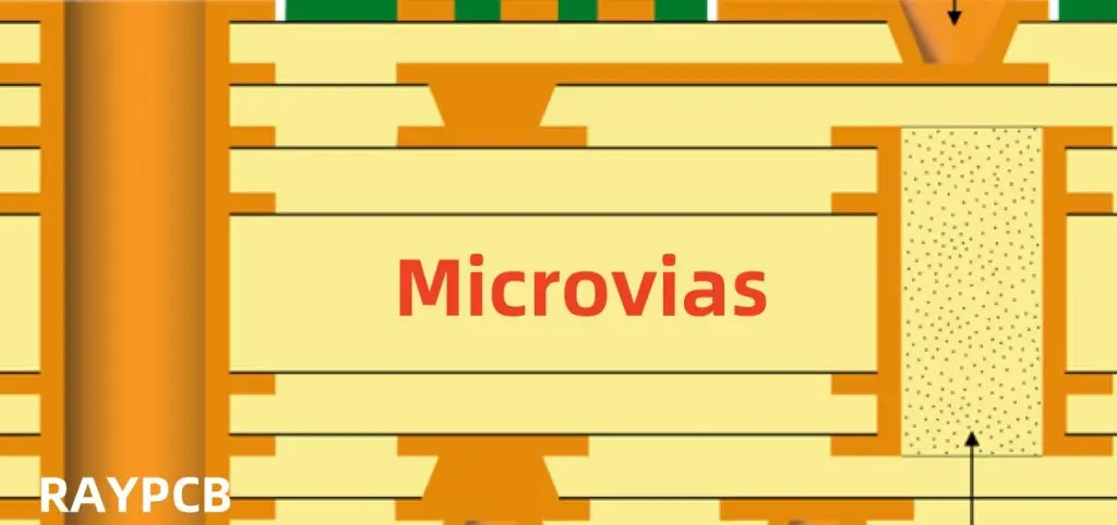
Vias are small holes drilled through PCB layers to create electrical connections between different layers of the board. These cylindrical pathways are plated with conductive material, typically copper, to ensure electrical continuity. The question of whether to fill these holes with additional material has become increasingly important as PCB designs become more complex and miniaturized.
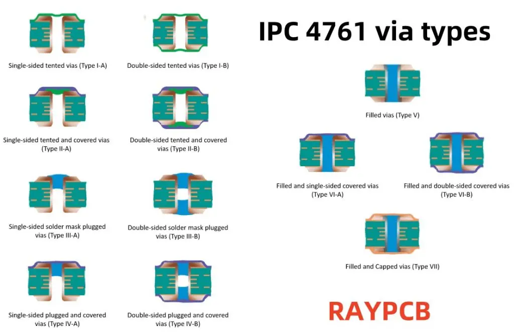
The filling process involves depositing material into the via barrel after the initial plating process. This can be done using various materials and techniques, each offering different benefits and serving specific purposes in the overall PCB design strategy.

Benefits of Filling Vias
Enhanced Structural Integrity
Filled vias provide superior mechanical strength compared to their unfilled counterparts. The filling material adds structural support that helps prevent via barrel cracking during thermal cycling, mechanical stress, or board flexing. This is particularly crucial in applications where the PCB will experience significant temperature variations or mechanical vibrations.
The additional structural support becomes even more critical in high-density interconnect (HDI) boards where via sizes are smaller and more susceptible to mechanical failure. Filled vias can withstand higher stress levels, making them ideal for aerospace, automotive, and military applications where reliability is paramount.
Improved Thermal Performance
Via filling can significantly enhance thermal management in PCB designs. When vias are filled with thermally conductive materials, they create efficient heat transfer pathways between layers. This is especially beneficial for high-power applications where heat dissipation is critical for maintaining component performance and preventing thermal damage.
Thermal vias filled with conductive materials can effectively transfer heat from hot components to heat sinks or ground planes, improving overall thermal performance. This capability is essential in LED lighting, power electronics, and high-frequency applications where thermal management directly impacts device longevity and performance.
Superior Electrical Performance
Filled vias offer several electrical advantages, particularly in high-frequency applications. The filling material can reduce parasitic inductance and capacitance, leading to improved signal integrity. This is crucial for high-speed digital circuits, RF applications, and precision analog designs where signal quality is paramount.
Additionally, filled vias provide better electromagnetic interference (EMI) shielding and can help maintain consistent impedance characteristics across the board. This results in cleaner signal transmission and reduced crosstalk between adjacent circuits.
Enhanced Reliability and Durability
The filling process creates a more robust interconnection that can withstand harsh environmental conditions. Filled vias are less susceptible to contamination, moisture ingress, and oxidation, which can compromise electrical performance over time. This enhanced reliability is particularly valuable in outdoor applications, marine environments, and industrial settings where PCBs face challenging conditions.
Drawbacks of Via Filling
Increased Manufacturing Costs
Via filling adds complexity to the manufacturing process, resulting in higher production costs. The additional processing steps, specialized materials, and quality control requirements can significantly increase the overall cost per board. For cost-sensitive applications or high-volume production runs, this cost increase may be prohibitive.
The cost impact becomes more pronounced when using specialized filling materials like thermally conductive compounds or when tight tolerance requirements necessitate additional processing steps.
Extended Manufacturing Time
The via filling process adds time to the production schedule. Depending on the filling method and material used, this can extend lead times by several days or even weeks. For projects with tight deadlines or rapid prototyping requirements, this additional time may be unacceptable.
The curing time for certain filling materials and the need for additional inspection steps can further extend manufacturing schedules, potentially impacting project timelines.
Process Complexity and Yield Issues
Via filling introduces additional variables into the manufacturing process, potentially affecting yield rates. Issues such as incomplete filling, void formation, or material shrinkage can lead to defective boards and reduced overall yield. This complexity requires more sophisticated process control and quality assurance measures.
Manufacturers must carefully control parameters such as temperature, pressure, and material viscosity to ensure consistent filling quality, adding complexity to the production process.
Types of Via Filling Materials
Conductive Filling
Conductive materials such as copper paste, silver-filled epoxy, or conductive polymers are used when electrical conductivity through the via is required. These materials maintain electrical connectivity while providing mechanical support and thermal conductivity benefits.
Conductive filling is essential for applications requiring current carrying capacity through the via or when the via serves as a thermal path for heat dissipation.
Non-Conductive Filling
Non-conductive materials like epoxy resins, polyimides, or specialized polymers are used when electrical isolation is desired while still providing mechanical support. These materials are often used in applications where via filling is primarily for structural reasons or to prevent contamination.
Non-conductive filling is common in applications where the via serves only as a mechanical support structure or when preventing solder wicking during assembly is important.
Soldermask-Defined Filling
In some applications, vias are filled with soldermask material during the soldermask application process. This approach provides a cost-effective way to fill vias while maintaining the overall manufacturing flow, though it offers limited structural and thermal benefits compared to dedicated filling materials.
When to Fill Vias
High-Reliability Applications
Applications requiring maximum reliability, such as aerospace, medical devices, or critical infrastructure systems, often benefit from via filling. The enhanced mechanical strength and protection from environmental factors justify the additional cost and complexity.
Thermal Management Requirements
When thermal management is critical, filled vias can provide essential heat transfer pathways. Power electronics, LED drivers, and high-performance computing applications often require filled thermal vias to maintain optimal operating temperatures.
High-Frequency and RF Applications
High-frequency designs benefit from the improved electrical characteristics of filled vias. The reduced parasitic effects and better impedance control can significantly improve signal integrity in RF and microwave applications.
Harsh Environmental Conditions
PCBs operating in challenging environments with exposure to moisture, chemicals, or extreme temperatures benefit from the protection offered by filled vias. The filling material helps prevent contamination and corrosion that could compromise long-term reliability.
When to Avoid Via Filling
Cost-Sensitive Applications
For consumer electronics or other cost-sensitive applications, the additional expense of via filling may not be justified if the performance benefits are not critical to the application’s success.
Simple, Low-Performance Designs
Basic circuits without high-frequency signals, significant thermal loads, or reliability requirements may not benefit from via filling. The added complexity and cost may not provide sufficient value in these applications.
Rapid Prototyping
During the design and prototyping phase, unfilled vias allow for faster turnaround times and lower costs, enabling more rapid design iterations and testing cycles.
Design Considerations and Best Practices
When deciding whether to fill vias, consider the specific requirements of your application, including performance specifications, environmental conditions, reliability requirements, and cost constraints. Work closely with your PCB manufacturer to understand their capabilities and recommendations for your specific design.
Consider the aspect ratio of your vias, as high aspect ratio vias may be more challenging to fill completely. Ensure that your design files clearly specify which vias should be filled and with what material to avoid manufacturing confusion.
Plan for the impact of via filling on your project timeline and budget early in the design process. This planning helps ensure that the decision aligns with overall project constraints and objectives.
Conclusion
The decision to fill or not fill vias in PCB design depends on multiple factors including application requirements, performance specifications, cost constraints, and manufacturing considerations. While via filling offers significant benefits in terms of reliability, thermal performance, and electrical characteristics, it also introduces additional costs and complexity.
Careful evaluation of your specific application requirements, working closely with experienced PCB manufacturers, and considering the long-term implications of your decision will help ensure the best outcome for your project. Whether you choose filled or unfilled vias, understanding the trade-offs involved will help you make an informed decision that balances performance, reliability, and cost effectively.

