Backplane Printed Circuit Boards (PCBs) are essential components in many electronic systems, serving as the backbone for interconnecting various modules and subsystems. These complex boards present unique challenges in design and fabrication due to their size, complexity, and high-performance requirements. This article will explore the key difficulties encountered in backplane PCB fabrication and provide valuable tips to overcome these challenges.
As we delve into the intricacies of backplane PCB fabrication, we’ll cover topics such as material selection, layer stackup, signal integrity, power distribution, and manufacturing considerations. By understanding these challenges and implementing the suggested solutions, engineers and PCB designers can create more reliable and efficient backplane systems.

2. Understanding Backplane PCBs
2.1 What is a Backplane PCB?
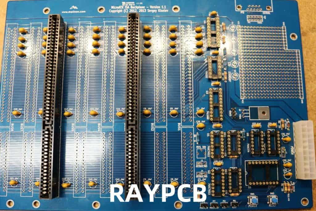
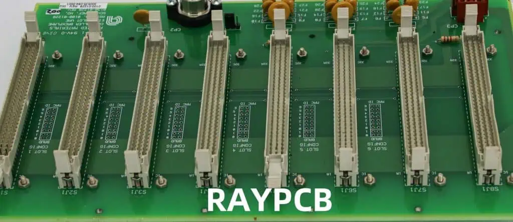
A backplane PCB is a large, complex circuit board that serves as the main interconnect for various daughtercards or modules in an electronic system. Backplanes are commonly used in:
- Telecommunications equipment
- Servers and data centers
- Industrial control systems
- Aerospace and defense applications
2.2 Key Characteristics of Backplane PCBs
Backplane PCBs have several distinguishing features:
| Characteristic | Description |
| Size | Typically larger than standard PCBs, often exceeding 24 inches in length |
| Layer Count | High layer count, frequently ranging from 20 to 40 layers or more |
| Thickness | Greater overall thickness due to multiple layers and rigid construction |
| Connectors | Numerous high-density connectors for daughtercard interfacing |
| Signal Integrity | Critical for high-speed data transmission across long traces |
| Power Distribution | Complex power planes to supply various voltages to multiple modules |
Understanding these characteristics is crucial for addressing the challenges in backplane PCB fabrication.
3. Key Difficulties in Backplane PCB Fabrication
3.1 Material Selection and Management
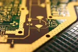
Choosing the right materials for backplane PCBs is critical due to their size and performance requirements.
3.1.1 Difficulty: Thermal Management
Backplanes generate significant heat due to their size and power requirements.
Tip: Select materials with good thermal conductivity and consider using thermal vias or embedded heat sinks.
3.1.2 Difficulty: Signal Integrity at High Frequencies
High-speed signals can degrade over long traces.
Tip: Use low-loss, high-frequency materials such as PTFE or low-loss FR-4 for critical signal layers.
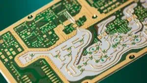
3.2 Layer Stackup Design
The complex layer stackup of backplane PCBs presents several challenges.
3.2.1 Difficulty: Impedance Control
Maintaining consistent impedance across multiple layers is challenging.
Tip: Use impedance-controlled stackup design tools and work closely with your PCB manufacturer to ensure feasibility.
3.2.2 Difficulty: Inter-layer Registration
Aligning multiple layers accurately becomes more difficult with increasing layer count.
Tip: Use buried and blind vias judiciously, and consider using sequential lamination techniques for better registration.
3.3 Signal Integrity
Maintaining signal integrity over long traces and through multiple connectors is a significant challenge in backplane design.
3.3.1 Difficulty: Signal Attenuation and Distortion
Long traces can lead to signal attenuation and distortion.
Tip: Implement pre-emphasis and equalization techniques, and consider using re-driver ICs for long signal paths.
3.3.2 Difficulty: Crosstalk
Dense routing and long parallel traces increase the risk of crosstalk.
Tip: Use differential signaling, maintain proper trace spacing, and implement guard traces or ground planes between critical signals.
3.4 Power Distribution
Providing clean, stable power to multiple modules is a complex task in backplane design.
3.4.1 Difficulty: Voltage Drop
Long power distribution paths can lead to significant voltage drops.
Tip: Use thick copper planes for power distribution and implement local voltage regulation on daughtercards.
3.4.2 Difficulty: Power Plane Resonance
Large power planes can exhibit resonance at certain frequencies.
Tip: Implement stitching capacitors and use segmented power planes to reduce resonance effects.
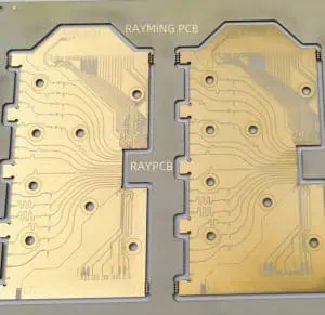
3.5 Manufacturing Considerations
The sheer size and complexity of backplane PCBs present unique manufacturing challenges.
3.5.1 Difficulty: Warpage and Dimensional Stability
Large PCBs are prone to warpage during manufacturing processes.
Tip: Use materials with low coefficient of thermal expansion (CTE) and work with manufacturers experienced in large board production.
3.5.2 Difficulty: Plating and Aspect Ratio
High layer counts result in high aspect ratio holes, which are difficult to plate uniformly.
Tip: Design with realistic aspect ratios (typically 10:1 or less) and consider using stacked microvias for high layer count designs.
4. Advanced Tips for Backplane PCB Fabrication
4.1 Simulation and Modeling
Extensive simulation is crucial for successful backplane design.
Tip: Use 3D electromagnetic simulation tools to model critical structures and validate design choices before fabrication.
4.2 Design for Manufacturing (DFM)
Incorporating DFM principles early in the design process can significantly improve manufacturability.
Tip: Develop and maintain a close relationship with your PCB manufacturer, and involve them early in the design process for feedback on manufacturability.
4.3 Test and Verification Strategies
Comprehensive testing is essential for ensuring backplane reliability.
Tip: Implement built-in self-test (BIST) features and design for testability to facilitate thorough testing during and after manufacturing.
5. Emerging Technologies in Backplane PCB Fabrication
5.1 High-Speed Materials
New materials are being developed to support higher frequencies and lower losses.
Tip: Stay informed about new material options and their characteristics, and consider using advanced materials for critical high-speed sections of the backplane.
5.2 Embedded Passives and Actives
Embedding components within the PCB structure can improve performance and save space.
Tip: Consider using embedded capacitors for power decoupling and embedded resistors for termination networks.
5.3 Optical Interconnects
As data rates continue to increase, optical interconnects are becoming more prevalent in backplane designs.
Tip: Evaluate the potential benefits of incorporating optical interconnects for high-speed data paths, especially for longer distances within the backplane.
6. Case Studies
6.1 Case Study 1: High-Speed Telecom Backplane
A telecommunications equipment manufacturer faced challenges with signal integrity in a 40-layer backplane design.
Solution:
- Implemented impedance-controlled differential pairs
- Used advanced low-loss materials for critical layers
- Incorporated re-driver ICs for long signal paths
Result: Achieved 25 Gbps data rates with excellent signal integrity across all channels.
6.2 Case Study 2: High-Reliability Aerospace Backplane
An aerospace company needed a highly reliable backplane for a mission-critical system.
Solution:
- Used polyimide materials for improved thermal stability
- Implemented redundant power and ground planes
- Designed for extreme environmental conditions
Result: Produced a backplane that passed rigorous qualification testing and met all reliability requirements.
7. Future Trends in Backplane PCB Fabrication
As technology continues to advance, several trends are shaping the future of backplane PCB fabrication:
- Increased adoption of optical interconnects
- Higher integration of smart features and embedded systems
- Advanced materials for improved signal integrity and thermal management
- Greater emphasis on environmental sustainability in materials and processes
Staying abreast of these trends will be crucial for designing competitive and future-proof backplane systems.
8. Conclusion
Backplane PCB fabrication presents numerous challenges due to the complexity, size, and high-performance requirements of these critical components. By understanding the key difficulties and implementing the tips and strategies outlined in this article, designers can create more reliable, efficient, and manufacturable backplane PCBs.
Remember that successful backplane design requires a holistic approach, considering electrical, mechanical, thermal, and manufacturing aspects. Continuous learning, collaboration with manufacturers, and leveraging advanced design and simulation tools are essential for staying at the forefront of backplane PCB fabrication technology.
9. Frequently Asked Questions (FAQ)
- Q: What is the maximum size for a backplane PCB? A: The maximum size for a backplane PCB depends on the manufacturer’s capabilities and the specific application requirements. Some manufacturers can produce boards up to 60 inches or more in length. However, as size increases, challenges related to warpage, handling, and uniformity become more significant. It’s essential to work closely with your PCB manufacturer to determine the feasible size for your specific design.
- Q: How many layers are typically used in a backplane PCB? A: Backplane PCBs typically have a high layer count, often ranging from 20 to 40 layers. Some complex designs may have even more layers. The exact number depends on factors such as the required interconnect density, signal integrity requirements, and power distribution needs. It’s important to balance the layer count with manufacturability and cost considerations.
- Q: What are the key considerations for signal integrity in backplane design? A: Key considerations for signal integrity in backplane design include:
- Proper impedance control
- Minimizing crosstalk through appropriate trace spacing and shielding
- Managing signal attenuation and distortion over long traces
- Implementing appropriate termination strategies
- Using differential signaling for high-speed signals
- Careful power and ground plane design to minimize noise
- Q: How do you address thermal management issues in backplane PCBs? A: Thermal management in backplane PCBs can be addressed through several strategies:
- Using materials with good thermal conductivity
- Implementing thermal vias to conduct heat from inner layers to external layers
- Designing with adequate copper weight for power and ground planes
- Incorporating embedded heat sinks or thermal management layers
- Ensuring proper airflow in the system design
- Using thermal simulation tools to identify and address hotspots
- Q: What are the advantages of using optical interconnects in backplane designs? A: Optical interconnects offer several advantages in backplane designs:
- Higher data rates over longer distances
- Immunity to electromagnetic interference
- Reduced power consumption compared to high-speed electrical interconnects
- Lower latency for long-distance connections within the backplane
- Potential for higher density interconnects However, optical interconnects also present challenges in terms of cost, integration, and interfacing with traditional electrical systems. The decision to use optical interconnects should be based on a careful analysis of the specific application requirements and overall system design.