In modern electronic systems operating at gigahertz frequencies, the design and implementation of printed circuit board (PCB) reference planes have become critical factors determining signal integrity and overall system performance. As digital signals transition faster and data rates increase, the electromagnetic behavior of transmission lines becomes increasingly important, making the reference plane one of the most crucial elements in high-speed PCB design.
Understanding Reference Planes in PCB Design
A reference plane in PCB design is typically a continuous copper layer that serves as a return path for electrical currents and provides a stable voltage reference for signals. These planes are usually designated as either power planes (carrying supply voltages like VCC) or ground planes (carrying ground potential). In multilayer PCBs, reference planes are strategically positioned to create controlled impedance transmission lines when combined with signal traces on adjacent layers.
The fundamental principle governing reference plane operation lies in electromagnetic field theory. When a high-speed signal propagates along a trace, it creates both electric and magnetic fields. The electric field terminates on the nearest reference plane, while the magnetic field forms closed loops. The reference plane provides the return current path that completes these magnetic field loops, essentially forming a transmission line structure with predictable electrical characteristics.

Electromagnetic Field Distribution and Signal Propagation
The proximity and characteristics of reference planes directly influence the electromagnetic field distribution around signal traces. In a microstrip configuration, where the signal trace runs on the surface layer with a reference plane beneath, the electric field lines emanate from the trace and terminate on the reference plane. The field distribution is asymmetrical, with some fields propagating through air and others through the dielectric substrate.
In stripline configurations, where the signal trace is embedded between two reference planes, the field distribution becomes more symmetrical and confined within the dielectric material. This confinement results in better signal integrity characteristics, including reduced electromagnetic interference (EMI) and improved impedance control.
The speed of signal propagation is fundamentally affected by the dielectric constant of the material between the signal trace and reference plane. The effective dielectric constant, which influences propagation velocity, depends on the field distribution, which in turn is controlled by the reference plane geometry and positioning.
Impedance Control and Characteristic Impedance
Reference planes play a pivotal role in determining the characteristic impedance of transmission lines. The characteristic impedance (Z₀) depends on the geometric relationship between the signal trace and reference plane, including trace width, thickness, height above the reference plane, and the dielectric constant of the intervening material.
For microstrip transmission lines, the characteristic impedance is primarily determined by the trace width-to-height ratio relative to the reference plane. Wider traces or closer proximity to the reference plane results in lower impedance, while narrower traces or greater distance increases impedance. This relationship allows designers to achieve specific impedance targets (commonly 50Ω for single-ended or 100Ω for differential signals) by adjusting these geometric parameters.
Maintaining consistent characteristic impedance along the entire signal path is crucial for preventing signal reflections. Any discontinuity in the reference plane, such as gaps, splits, or plane changes, can cause impedance variations that lead to signal reflections, ringing, and degraded signal quality.
Return Current Path and Current Distribution

High-speed signals require a complete circuit for current flow, with the return current naturally following the path of least impedance back to the source. In well-designed PCBs, this return current flows on the reference plane directly beneath the signal trace, creating a tightly coupled transmission line structure.
The return current distribution on the reference plane is not uniform but concentrated in a region directly under the signal trace. The current density decreases rapidly with distance from the trace centerline, with most of the return current flowing within a width approximately equal to twice the trace height above the reference plane.
When reference plane discontinuities occur, such as splits or gaps, the return current must find alternative paths. This forces the current to take longer routes around the discontinuity, increasing loop inductance and potentially causing signal integrity problems. The increased loop area also enhances the potential for EMI generation and susceptibility.
Effects of Reference Plane Discontinuities
Reference plane discontinuities represent one of the most significant challenges in high-speed PCB design. These discontinuities can take various forms, including plane splits for power distribution, via antipads, connector areas, and component placement regions where the reference plane is removed.
When a high-speed signal crosses a gap in its reference plane, several detrimental effects occur. The impedance typically increases due to the reduced coupling between signal and reference, causing reflections at the discontinuity boundaries. The return current must find alternative paths, often through decoupling capacitors or other reference planes, creating current loops with higher inductance and greater EMI potential.
Plane splits are particularly problematic when high-speed signals must cross them. The return current cannot flow directly beneath the signal trace, forcing it to find paths around the split through connections between different plane regions. This creates substantial loop inductance and can cause significant signal degradation.
Via Structures and Layer Transitions
Modern multilayer PCBs require signals to transition between layers through vias, creating complex interactions with reference planes. When a signal via passes through multiple layers, it typically encounters several reference planes, each potentially at different electrical potentials.
The via structure itself creates impedance discontinuities due to its different geometry compared to surface traces. The via barrel presents a different impedance environment, while the via pad and antipad (clearance hole in reference planes) further complicate the electromagnetic field distribution.
Return current behavior becomes particularly complex in via transitions. When a signal changes layers, its return current must also transition to the appropriate reference plane for the new layer. This transition occurs through stitching vias or decoupling capacitors connecting the reference planes. Without proper return current management, signal quality degrades significantly.
Power Distribution Network Integration
Reference planes serve dual purposes in modern PCB designs, functioning both as signal references and as part of the power distribution network (PDN). Power planes distribute supply voltages throughout the PCB while simultaneously serving as reference planes for high-speed signals.
The PDN characteristics directly impact signal integrity through several mechanisms. Power plane impedance affects the stability of the reference voltage, with high impedance potentially causing reference bounce and signal degradation. The decoupling capacitor network, designed to maintain low PDN impedance, also provides return current paths for signals crossing plane discontinuities.
Simultaneous switching noise (SSN) represents another critical interaction between power distribution and signal integrity. When multiple signals switch simultaneously, they create current transients in both power and ground planes. If the PDN impedance is too high at the switching frequencies, voltage fluctuations occur that can affect signal timing and noise margins.
Crosstalk and Electromagnetic Interference
Reference planes significantly influence crosstalk between adjacent signals. The proximity of a reference plane affects both electric and magnetic field coupling between traces. Closer reference planes generally reduce crosstalk by providing better field confinement and shorter return current paths.
The reference plane also acts as a shield, reducing electromagnetic radiation from high-speed signals and providing protection against external interference. Continuous reference planes are particularly effective at containing electromagnetic fields within the PCB stackup.
However, reference plane discontinuities can actually enhance crosstalk in some situations. When return currents are forced to take circuitous paths around plane gaps, the enlarged current loops can couple more strongly with other circuits, potentially increasing both crosstalk and EMI.
Design Guidelines and Best Practices
Effective reference plane design requires careful attention to several key principles. Maintaining continuous reference planes under all high-speed signals provides the most predictable transmission line behavior. When plane splits are necessary, they should be oriented perpendicular to signal flow to minimize the crossing distance.
Via stitching becomes crucial for managing return currents in multilayer designs. Stitching vias should be placed adjacent to signal vias to provide low-inductance return current paths. The spacing and number of stitching vias should be determined based on the signal frequencies and required loop inductance.
Layer stackup design should prioritize signal-reference plane pairs, with each high-speed signal layer directly adjacent to a reference plane. This arrangement provides optimal impedance control and signal integrity performance. Mixed power and ground reference planes can be used effectively, but require careful PDN design to maintain low impedance at signal frequencies.
Advanced Considerations and Future Trends
As signal speeds continue to increase into the tens of gigahertz range, reference plane design becomes even more critical. Advanced effects such as surface roughness, causal dielectric properties, and frequency-dependent losses must be considered in reference plane design.
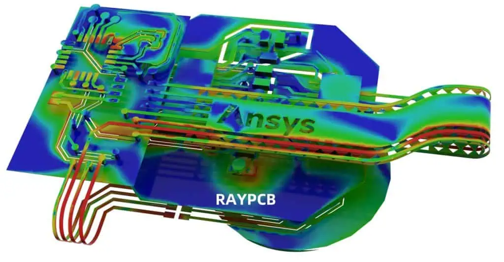
Three-dimensional electromagnetic simulation tools have become essential for predicting reference plane effects in complex designs. These tools enable designers to optimize reference plane configurations before fabrication, reducing the need for costly design iterations.
Emerging technologies such as embedded components and advanced packaging techniques create new challenges for reference plane design. These approaches require novel solutions for maintaining signal integrity while achieving higher integration densities.
The impact of printed circuit board reference planes on high-speed signal transmission cannot be overstated. As digital systems push toward higher frequencies and faster edge rates, the electromagnetic behavior governed by reference plane design becomes the limiting factor in achievable performance. Understanding and properly implementing reference plane design principles is essential for successful high-speed digital system development in contemporary electronic design.