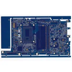
Layer: 26 Layer PCB
Material: Tachyon 100G
PCB Thickness: 3.5±0.35mm
Copper thickness: 1/3OZ
Min. LW/LS: 0.118/0.051mm
Min. hole Size:0.2mm
Surface Finish: ENIG (Immersion Gold)
Application: Industrial Control Board
Estimate 26 Layer PCB Cost, Pls send PCB File to Sales@raypcb.com with Requirement.
3.5mm Thickness 26 Layer High Speed ENIG Industrial Control PCB
In the world of industrial control systems, printed circuit boards (PCBs) play a crucial role in ensuring reliable and efficient operation. This article delves into the specifics of a 3.5mm thickness, 26 layer high speed ENIG (Electroless Nickel Immersion Gold) industrial control PCB. We’ll explore its unique features, advantages, and applications, as well as the technical considerations involved in its design and manufacturing.
Understanding the PCB Specifications
Thickness and Layer Count
The PCB under discussion boasts impressive specifications:
| Feature | Specification |
|---|---|
| Thickness | 3.5mm |
| Layer Count | 26 layers |
| Surface Finish | ENIG |
| Application | Industrial Control |
These specifications indicate a highly complex and robust PCB designed for demanding industrial environments.
High Speed Considerations
The term “high speed” in PCB design typically refers to circuits operating at frequencies above 100 MHz or with rise times less than 1 nanosecond. For this industrial control PCB, high speed design is crucial for:
- Rapid data processing
- Real-time control systems
- High-frequency signal integrity
ENIG Surface Finish
What is ENIG?
ENIG stands for Electroless Nickel Immersion Gold. This surface finish consists of:
- A layer of nickel (typically 3-6 μm thick)
- A thin layer of gold (typically 0.05-0.1 μm thick)
Advantages of ENIG for Industrial Control PCBs
| Advantage | Description |
|---|---|
| Durability | Resistant to oxidation and corrosion |
| Flatness | Excellent for fine-pitch components |
| Shelf Life | Long shelf life without degradation |
| Multiple Soldering | Supports multiple soldering cycles |
| Compatibility | Works well with various soldering methods |
Design Considerations for 26 Layer PCBs
Layer Stack-up
Designing a 26 layer PCB requires careful consideration of the layer stack-up. A typical arrangement might include:
- Multiple power and ground planes
- Several signal layers for different purposes (high-speed, low-speed, analog, digital)
- Dedicated layers for impedance control
Impedance Control
In high-speed designs, maintaining consistent impedance is crucial. This 26 layer PCB likely incorporates:
- Stripline configurations for internal layers
- Microstrip configurations for outer layers
- Precise calculations for trace width and spacing
Signal Integrity
To maintain signal integrity in this complex PCB:
- Proper routing techniques are employed
- Layer transitions are minimized
- Return paths are carefully managed
- Crosstalk is mitigated through intelligent trace placement and shielding
Manufacturing Challenges
Drilling and Aspect Ratio
With a thickness of 3.5mm and 26 layers, drilling becomes a significant challenge. The aspect ratio (board thickness to hole diameter) must be carefully managed to ensure reliable plated through-holes.
Registration
Aligning 26 layers accurately requires advanced manufacturing techniques and equipment. Misregistration can lead to:
- Impedance mismatches
- Crosstalk issues
- Potential short circuits or open circuits
Material Selection
The choice of material for this PCB is critical. Considerations include:
- Dielectric constant and loss tangent for high-speed performance
- Thermal stability for industrial environments
- Coefficient of thermal expansion (CTE) for reliability
Applications in Industrial Control
This 3.5mm thickness, 26 layer high speed ENIG PCB is well-suited for advanced industrial control applications, such as:
- Complex automation systems
- High-performance robotics controllers
- Advanced process control equipment
- Industrial IoT (Internet of Things) gateways
- High-reliability aerospace and defense systems
Advantages of This PCB Design
The unique specifications of this PCB offer several advantages:
- High component density due to the large number of layers
- Excellent signal integrity for high-speed operations
- Robust design suitable for harsh industrial environments
- Long-term reliability due to the ENIG finish
- Flexibility in circuit design and power distribution
Future Trends
As industrial control systems continue to evolve, we can expect to see:
- Even higher layer counts for increased functionality
- Integration of embedded components within the PCB structure
- Advanced materials for improved thermal management and signal integrity
- Implementation of AI and machine learning capabilities directly on the board
Conclusion
The 3.5mm thickness, 26 layer high speed ENIG industrial control PCB represents the cutting edge of PCB technology for industrial applications. Its complex design, robust construction, and advanced surface finish make it an ideal choice for demanding control systems that require high performance, reliability, and longevity.
Frequently Asked Questions (FAQ)
- Q: Why is a 26 layer PCB necessary for industrial control applications? A: A 26 layer PCB allows for high component density, complex routing schemes, and dedicated power and ground planes, which are often required in sophisticated industrial control systems that demand high performance and reliability.
- Q: What advantages does the 3.5mm thickness provide? A: The 3.5mm thickness enhances the PCB’s mechanical stability, improves heat dissipation, and allows for more robust connections, all of which are beneficial in industrial environments that may involve vibration, temperature fluctuations, and high-power components.
- Q: How does the ENIG surface finish contribute to the PCB’s performance? A: ENIG provides excellent surface planarity for fine-pitch components, offers good solderability, resists oxidation, and maintains a long shelf life. These properties ensure reliable connections and long-term performance in industrial control applications.
- Q: What are the main challenges in manufacturing a 26 layer PCB? A: The primary challenges include achieving proper registration across all layers, managing the high aspect ratio for through-holes, ensuring consistent impedance control, and selecting appropriate materials that can withstand the manufacturing process while meeting performance requirements.
- Q: How does this PCB design support high-speed operations? A: The high layer count allows for dedicated high-speed signal layers, controlled impedance routing, and effective power distribution. The ENIG finish and careful layer stack-up design contribute to maintaining signal integrity at high frequencies.