In the world of electronic design, decoupling capacitance plays a crucial role in maintaining signal integrity and power distribution. Traditionally, this has been achieved through the use of discrete capacitor components placed strategically on printed circuit boards (PCBs). However, as electronic devices continue to shrink in size and increase in complexity, engineers are seeking innovative ways to obtain decoupled capacitance without relying on additional components. This article explores the concept of achieving decoupled capacitance without components, focusing on techniques such as buried capacitance, integrated capacitance, and other emerging technologies.
Understanding Decoupled Capacitance
What is Decoupled Capacitance?
Decoupled capacitance refers to the practice of providing local charge storage near active devices on a PCB to mitigate the effects of rapid current demands and maintain stable voltage levels. This is typically achieved by placing capacitors close to the power pins of integrated circuits (ICs) to supply instantaneous current and reduce noise on power supply lines.
The Importance of Decoupling in Electronic Circuits
Decoupling is essential for several reasons:
- Noise reduction: It helps suppress high-frequency noise on power supply lines.
- Voltage stability: It maintains steady voltage levels during rapid current transitions.
- EMI reduction: It minimizes electromagnetic interference (EMI) emissions from the circuit.
- Improved performance: It enhances the overall performance and reliability of electronic systems.
Traditional Methods of Decoupling
Conventionally, decoupling has been achieved using discrete capacitor components. Here’s a brief overview of traditional decoupling methods:
| Method | Description | Advantages | Limitations |
| Surface-mount capacitors | Small capacitors placed close to IC power pins | Easy to implement, wide range of values available | Occupies board space, parasitic inductance |
| Multi-layer ceramic capacitors (MLCCs) | Compact capacitors with low ESR and ESL | High capacitance density, good high-frequency performance | Still requires board real estate, potential for cracking |
| Capacitor arrays | Integrated packages containing multiple capacitors | Saves space compared to individual capacitors | Limited flexibility, potentially higher cost |
| Decoupling networks | Combination of capacitors with different values | Provides decouplin |
While these methods have served the industry well, the push for miniaturization and higher performance has led to the exploration of component-less decoupling solutions.
Buried Capacitance Technology

Concept of Buried Capacitance
Buried capacitance is an innovative approach to achieving decoupled capacitance without the need for discrete components. It involves integrating capacitive structures directly into the PCB stack-up, creating a distributed capacitance throughout the board.
How Buried Capacitance Works
The principle behind buried capacitance is to create a thin dielectric layer between power and ground planes within the PCB. This forms a large, distributed capacitor that spans the entire board area. Here’s how it works:
- Thin dielectric layer: A very thin (typically less than 10 μm) layer of high-permittivity material is used between power and ground planes.
- Large area: The entire overlap area of the power and ground planes contributes to the capacitance.
- Distributed nature: The capacitance is spread across the board, providing localized decoupling wherever needed.
Advantages of Buried Capacitance
Buried capacitance offers several benefits over traditional decoupling methods:
- Space-saving: Eliminates the need for numerous surface-mount capacitors, freeing up valuable board real estate.
- Improved performance: Lower inductance due to the distributed nature of the capacitance.
- Noise reduction: More effective at suppressing high-frequency noise.
- Simplified design: Reduces the complexity of component placement and routing.
- Cost-effective: Can potentially reduce overall manufacturing costs by eliminating components.
Implementation Challenges
While buried capacitance technology offers significant advantages, it also presents some challenges:
- Specialized materials: Requires high-permittivity, thin dielectric materials.
- Manufacturing process: Demands precise control of layer thicknesses and material properties.
- Design tools: Necessitates advanced PCB design tools that can model and simulate buried capacitance effects.
- Limited capacitance values: The achievable capacitance is constrained by board area and material properties.
Integrated Capacitance in Silicon
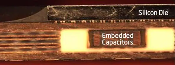
On-Chip Decoupling Capacitance
Another approach to obtaining decoupled capacitance without discrete components is to integrate it directly into the silicon of integrated circuits. This method, known as on-chip decoupling, involves creating capacitive structures within the IC itself.
Types of Integrated Capacitors
There are several types of integrated capacitors used for on-chip decoupling:
| Type | Description | Advantages | Limitations |
| MOS capacitors | Uses the gate oxide of MOS transistors | High capacitance density, compatible with standard CMOS processes | Voltage-dependent capacitance |
| Metal-insulator-metal (MIM) capacitors | Utilizes metal layers separated by a thin dielectric | Good linearity, high Q-factor | Requires additional process steps |
| Poly-insulator-poly (PIP) capacitors | Uses polysilicon layers as electrodes | Compatible with older process nodes | Lower capacitance density compared to MIM |
| Deep trench capacitors | Vertical structures etched into the silicon substrate | Very high capacitance density | Complex manufacturing process |
Benefits of On-Chip Decoupling
Integrating decoupling capacitance on-chip offers several advantages:
- Proximity: Capacitance is located extremely close to the circuits that need it.
- Reduced parasitics: Minimizes inductance and resistance associated with external connections.
- Improved high-frequency performance: Better response to rapid current transients.
- Simplified PCB design: Reduces the need for external decoupling components.
Limitations and Considerations
While on-chip decoupling is beneficial, it has some limitations:
- Limited capacitance: The amount of on-chip capacitance is constrained by die area and process technology.
- Cost: Integrating large amounts of capacitance can increase die size and cost.
- Process complexity: Some integrated capacitor types require additional manufacturing steps.
- Design complexity: Requires careful consideration during IC design and layout.
Advanced PCB Materials and Structures for Component-less Decoupling
High-k Dielectric Materials
One of the key enablers of component-less decoupling is the development of high-k dielectric materials. These materials have a higher dielectric constant (k) than traditional PCB substrates, allowing for greater capacitance in a given area.
Properties of High-k Materials
Here’s a comparison of some common PCB dielectric materials and their properties:
| Material | Dielectric Constant (k) | Typical Thickness | Capacitance Density |
| FR-4 | 4.0-4.5 | 100-200 μm | Low |
| High-k Laminates | 10.-30 | 50-100 μm | Medium |
| Ceramic-filled Epoxy | 30-50 | 25-75 μm | High |
| Thin-film Ceramics | 100-1000 | 1-10 μm | Very High |
Advantages of High-k Materials for Decoupling
- Increased capacitance density
- Improved power integrity
- Reduced layer count in PCB stack-ups
- Enhanced high-frequency performance
Challenges in Implementation
- Higher material costs
- Potential for increased signal loss
- Manufacturing process adaptations
- Design tool limitations for accurate modeling
Embedded Planar Capacitance
Embedded planar capacitance takes the concept of buried capacitance further by incorporating specialized materials and structures within the PCB stack-up.
Structure of Embedded Planar Capacitance
- Ultra-thin dielectric layer (typically 2-20 μm)
- Large area copper planes on both sides of the dielectric
- Integration into standard PCB manufacturing processes
Benefits of Embedded Planar Capacitance
- Very high capacitance density (up to 10 nF/cm²)
- Excellent high-frequency decoupling performance
- Reduced PCB layer count
- Improved signal integrity and EMI suppression
Design Considerations
- Careful power plane segmentation
- Proper via placement for effective charge distribution
- Consideration of thermal management implications
- Integration with other PCB design elements (e.g., signal routing)
Interdigitated Capacitance Structures
Interdigitated capacitance structures offer another approach to achieving component-less decoupling by utilizing the PCB’s existing copper layers.
How Interdigitated Structures Work
- Alternating finger-like extensions of power and ground planes
- Increased edge coupling between adjacent fingers
- Utilization of fringing electric fields for capacitance
Advantages of Interdigitated Structures
- Can be implemented with standard PCB materials
- No need for specialized ultra-thin dielectrics
- Flexible design options for targeted decoupling
- Compatible with both rigid and flexible PCB technologies
Design Trade-offs
- Reduced plane area for current distribution
- Potential for increased crosstalk in nearby signal traces
- Complexity in optimizing finger dimensions and spacing
- Limited total capacitance compared to other methods
Hybrid Approaches
In practice, achieving optimal decoupling often involves a combination of techniques. Hybrid approaches leverage the strengths of multiple methods to create a comprehensive decoupling solution.
Combining Techniques
- Buried capacitance + strategic discrete components
- On-chip decoupling + embedded planar capacitance
- Interdigitated structures + high-k materials
Benefits of Hybrid Solutions
- Tailored decoupling for different frequency ranges
- Optimized performance-cost trade-off
- Flexibility in addressing specific design requirements
- Improved overall system performance
Design and Simulation Techniques
Implementing component-less decoupling requires advanced design and simulation techniques to ensure optimal performance.
Electromagnetic Field Simulation
Electromagnetic field simulation is crucial for accurately predicting the behavior of component-less decoupling structures.
Key Aspects of EM Simulation
- Full-wave analysis of PCB stack-up
- Modeling of complex material properties
- Extraction of distributed capacitance and inductance
- Prediction of resonances and anti-resonances
Tools and Methodologies
- Finite Element Method (FEM) solvers
- Method of Moments (MoM) tools
- Hybrid simulation techniques
- Multi-physics simulations for thermal considerations
Power Integrity Analysis
Power integrity analysis is essential for evaluating the effectiveness of component-less decoupling solutions.
Elements of Power Integrity Analysis
- DC IR drop analysis
- AC impedance profiling
- Time-domain transient simulations
- Frequency-domain resonance analysis
Performance Metrics
| Metric | Description | Target Values |
| Target Impedance | Maximum acceptable power distribution network impedance | Typically 1-10 m惟 |
| Voltage Ripple | Peak-to-peak voltage variation on power rails | < 5% of nominal voltage |
| Resonant Frequencies | Frequencies at which the power delivery network resonates | Should be outside operating frequency range |
| Decoupling Effectiveness | Measure of how well the decoupling solution suppresses noise | > 20 dB atten |
Optimization Techniques
Optimizing component-less decoupling designs often requires sophisticated algorithms and methodologies.
Optimization Approaches
- Genetic algorithms for layout optimization
- Machine learning-based material selection
- Multi-objective optimization for balancing performance and cost
- Sensitivity analysis for identifying critical design parameters
Design for Manufacturability (DFM) Considerations
- Layer stack-up optimization
- Via placement and sizing strategies
- Copper balancing techniques
- Alignment with PCB fabrication capabilities
Practical Implementation and Case Studies
To illustrate the real-world application of component-less decoupling, let’s examine some case studies and practical implementation strategies.
Case Study 1: High-Speed Digital PCB
In this case study, a high-speed digital PCB for a telecommunications application utilized embedded planar capacitance to achieve superior decoupling performance.
Design Approach
- Utilization of 4 μm thick high-k dielectric layer
- Strategic segmentation of power planes
- Optimized via placement for charge distribution
- Hybrid solution with minimal strategic discrete capacitors
Results
- 50% reduction in discrete decoupling capacitors
- 30% improvement in power supply noise rejection
- 20% reduction in overall PCB thickness
- Significant improvement in signal integrity margins
Case Study 2: Mixed-Signal Automotive PCB
This case study focuses on a mixed-signal automotive PCB that employed a combination of buried capacitance and interdigitated structures.
Implementation Strategy
- Buried capacitance for global power distribution
- Interdigitated structures for localized high-frequency decoupling
- Careful isolation of analog and digital power domains
- Use of EM simulation for optimizing interdigitated patterns
Outcomes
- Elimination of 80% of surface-mount decoupling capacitors
- Improved EMI performance, meeting stringent automotive standards
- Enhanced reliability due to reduced component count
- 15% reduction in overall PCB cost
Best Practices for Implementation
Based on these case studies and industry experience, here are some best practices for implementing component-less decoupling:
- Start with accurate EM and power integrity simulations
- Consider hybrid approaches for optimal performance
- Pay close attention to manufacturing tolerances and their impact
- Validate designs through prototyping and extensive testing
- Stay informed about emerging materials and technologies
- Collaborate closely with PCB manufacturers to ensure feasibility
Future Trends and Emerging Technologies
The field of component-less decoupling is continuously evolving. Here are some future trends and emerging technologies to watch:
- Advanced nanomaterials for ultra-high-k dielectrics
- 3D-printed embedded capacitance structures
- Integration of decoupling solutions with active power management systems
- Machine learning-driven optimization of decoupling designs
- Adoption of component-less decoupling in flexible and stretchable electronics
As these technologies mature, we can expect even more efficient and effective component-less decoupling solutions in the future.
Frequently Asked Questions (FAQ)
- Q: Can component-less decoupling completely eliminate the need for discrete capacitors? A: While component-less decoupling can significantly reduce the number of discrete capacitors, it may not completely eliminate them in all cases. Some designs may still require a few strategic discrete components for optimal performance, especially at very high frequencies or for bulk decoupling.
- Q: How does the cost of component-less decoupling compare to traditional methods? A: The cost comparison depends on various factors, including production volume, PCB complexity, and specific implementation. While component-less solutions may have higher initial material costs, they often lead to overall cost savings through reduced component count, improved reliability, and simplified assembly processes.
- Q: Are there any reliability concerns with component-less decoupling techniques? A: Generally, component-less decoupling can improve reliability by reducing the number of solder joints and potential points of failure. However, it’s crucial to consider factors such as thermal cycling, moisture sensitivity, and long-term stability of the specialized materials used.
- Q: How does component-less decoupling affect PCB manufacturability? A: Component-less decoupling may require adjustments to standard PCB manufacturing processes, particularly when using very thin dielectric layers or specialized materials. Close collaboration with PCB manufacturers is essential to ensure producibility and yield.
- Q: Can component-less decoupling techniques be applied to flexible PCBs? A: Yes, many component-less decoupling techniques can be adapted for flexible PCBs. Techniques like interdigitated structures and some forms of buried capacitance are particularly suitable for flexible circuits, offering decoupling solutions without compromising flexibility.
This concludes the article on how decoupled capacitance can be obtained without components. The content covers the concept, various techniques, implementation challenges, design considerations, and future trends in component-less decoupling for PCBs.