What Is PCB Current Calculator, its Importance, And How To Use?

PCB Current Calculator

The PCB standard of IPC-2221 contains various requirements and specifications for the manufacture and design of circuit boards. Today, there are various web-based calculators that follow this standard. Apart from calculating the annular ring and impedance, it also focuses on the trace width, temperature rise, and trace current. Both standards, IPC-2152 and IPC-2221, include guidelines regarding designing the PCB for thermal tolerance. Both standards have a distinctly detailed debate over the applicability and usage of both standards. 

If you decide to choose the IPC-2221 standard, then donโ€™t be afraid. We have made a very simple and easy-to-use PCB calculator that helps to determine the limits of trace width in a given limit of heat. If you use Altium Designer, you can find these features in the Circuit Board Editor while working on the PCB routing.

Types Of PCB Current Calculators and Trace Width 

PCB-Trace-Width-Calculator

The trace width of PCB can be determined through various distinct calculators. All these PCB calculators follow the standard of the PCB industry. These PCB industry standards follow the guidelines for calculations. Both the IPC-2221 and IPC-2152 standards are widely used in commercial and industrial applications. 

1. IPC 2221 PCB Trace Width

The calculator IPC-2221 uses a graph and an equation to calculate the current of the PCB track. The formula stands for I=kฮ”TbAc.

In this formula, the Visible traces represent the K which has a value of 0.0048, and internal traces also represent the K which has a value of 0.024. ฮ”T represents the change in temperature in Celsius. The B value equals 0.44, and the C value equals 0.725. Whereas, A represents the area of cross-section.

The IPC-2221 calculator only uses a specific range of all values to calculate the PCB trace width. The range of current falls between 35 and 0 amperes, track width between 10.16 to 0 mm, the width of copper between 3 to 0.5 oz, and the rise in temperature between 100 to 10 oC. It does not give accurate results if the value changes from these specific ranges.

2. IPC 2152 PCB Trace Width

The Calculator IPC-2152 uses an advanced and recent standard type for the calculation. This gives a more precise and accurate calculation of Max capacity of trace current. It uses advanced technical methods. The formula of this calculator does not seem simple as compared to the calculator IPC-2221. To determine the unorganized area of the cross-section, it uses a universal graph.

However, this IPC-2152 calculator uses various types of parameters to create a number of modifiers. Therefore, the parameters include the thickness of the trace for passing, the distance between the tracks and copper planes, as well as the thermal conductivity of the PCB.

Whatโ€™s In IPC-2221 in Electronics Industry?

An IPC-2221 is a type of standard for the acceptance and qualification of PCBAs and PCBs. The standards demand some requirements and specifications to design a PCB, which ensure the manufacturability, reliability, and safety of a PCB. These standards come in generic standards. At the same time, you can specify a certain type of standard that applies to the PCB used in the whole series of 2220.

The IPC-2221 calculator uses the above formula to calculate the width of the PCB trace, which is needed to keep the level of temperature below a certain range. In simple words, you just have to enter the weight of the copper in the calculator. As a result, it gives you the value of trace width, which is required within the given temperature rise and current. 

Does the IPC-2221 calculator exist in an online system of CAD? Well, yes, the user of Altium Designer can avail of this tool in the tools of routing present in the window of PCB Editor. To analyze the trace width, just select the trace and then expand the information in the NEt Data area present in the Panel of Properties.

PCB Current Calculator: IPC-2221 Formula

FULL PCB MANUFACTURING Quote

The formulas mentioned above have some things to note to find which show precise and accurate results. 

  1. The formula is chart-based.
  2. The formula predicts that the PCB lies at STP in an open environment with air.
  3. The prototypes before using a trace of only thick PCBs and no extra copper planes to disperse heat.
  4. They treat multiple parallel closer traces as one bug trace to pass the current.
  5. If the thinness of the board falls below 30 mils, it recommends to derate it by 15% rather than 10%.
  6. Higher thermal capability substrates have distinct limits of trace and current width than a conventional laminate of epoxy-fiberglass.

This means that the IPC-2221 calculator does not give accurate results when it comes to modern PCBs. In simple words, the value of current capacity changes if you put an additional plane and copper around the trace, and it gives an underestimated value. On the other hand, it gets reversed with a minimum width of trace and gives an overestimated value. Remember these points, as it helps in calculating an accurate trace width.

Because of the nuisance of this standard with modern PCBs, designers and engineers were forced to create an advanced standard that gives higher efficiency, accuracy, and specificity. And then comes the IPC-2152 standard.

IPC-2221 Vs. IPC2152: Which is the Best to Use?

All online calculators have some limitations. The calculator IPC-2221 also falls in this category. Itโ€™s the fact that the IPC-2221 calculator gives an overestimated value of minimum trace width. Therefore, the standard IPC-2152 calculator expands the data to add numerous nomographs which determine the current limits, temperature rise, and trace width.

Currents a PCB Trace Carry and its Importance


The PCB trace current capacity limitation is one of the main problems which arise in various electronic projects. In many home projects, the value never exceeds the maximum limit, which seems better.

The calculator helps greatly in determining the current capacity of PCB trace yet gives a hard time in handling the charts. As the max PCB trace, the current capacity is linked with the operational temperature and width. 

Importance of Using the PCB Current Calculator Trace Width

The current calculator of PCB trace is an easy-to-use tool. It is divided into Output and Input sections which makes it easy to put data and obtain the results. The fields in this calculator include the following:

  1. The Internal and External trace location according to the substrate of PCB.
  2. The width of the trace represents the distance.
  3. The thickness of the trace represents the horizontal length of the PCB trace.
  4. The Max temperature rise represents the maximum value of a difference between the ambient temperature and PCB trace.

However, in advanced features:

  1. The surrounding temperature.
  2. The trace length from start to end.
  3. The Max PCB traces current capacity.
  4. The trace cross-sectional area.
  5. The temperature of trace while operation.
  6. The trace resistance at Max PCB traces current capacity.
  7. The drop of voltage for the max current and calculated resistance value.
  8. The dissipation of power at the max rate of current capacity.

Guidelines and Tips for Using the PCB Current Calculator 

The current that flows through the track and the specification of design determines the trace width of the PCB. However, it follows a specific rule. The minimum value of the traceroute ranges from 10 mm/A. This goes well for a 1.0 oz/ft2 thickness of copper.

The calculation of trace width is a complex process. That is why it requires some rules to understand for calculating the trace width of PCB. The circuit works well on max current with ambient temperature, the thickness of the trace, and the trace measurement unit. These values depict the input range of trace width.

When you add these values inside the calculator of trace width, it gives back some output values. This output value represents the PCB trace width. The datasheet shows all the figures of input. It does not work with guess figures. All PCB requires this information to calculate the trace width.

The calculator does not work well and gives no output if the input value is wrong. You may also need a magnifying glass so that you can see the exact values on the PCB.

Confirming the Efficient Trace Width with PCB Calculator 

ยท Standard Track Width

First, decide the track size for the PCB in your design. Too thin, narrow, and close tracks lead to short circuits. At the same time, too much spacing between the tracks must need some restriction on the track number. In such scenarios, incorporate extra plane layers in the PCB to make sure the routing of the PCB.

ยท Circuit Pad Shapes

The libraries of components typically possess PCB libraries for the schematic and footprint of different electrical components. Although, it depends on the process of PCB manufacturing. Therefore, you have to select the process of manufacturing before beginning the design process. This way, you can select the appropriate size of pads and later on incorporate it over the CAD system of PCB. 

ยท Track the Size of Lines

PCBs Possess a thin track of line which limits the carrying capacity of current. That is why we must consider the size of the trace for any route that carries a power current instead of lesser signal levels.

ยท Dimensions Of Hole & Pad

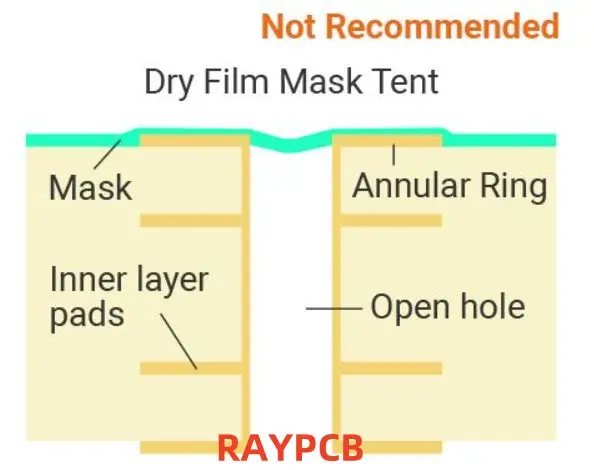
It’s important to decide on the pad and the hole dimension once you begin the design of the PCB. It may vary according to various situations. Sometimes, the ratio of pad-to-hole falls to 1:8. Sometimes, it measures when the pad is bigger than the hole. The manufacturers of PCBs have their own set of standards according to the usage of the application. The ratio gets more crucial as the size of the pads, and the hole decreases.

Factors to Think about When Developing PCB Trace Width 

The trace width of a PCB directly affects the functionality of a PCB in many ways. However, we have a few factors to take into account while determining the value of trace width.

ยท Signal Integrity & Electrical Performance

The majority of PCB digital routing possesses the default trace width value, yet some may need distinct sizes. For instance, the steady impedance net of traces needs the evaluation of trace width on the basis of the stack up of PCB layer consideration. 

In most cases, analog routing requires the PCB trace width according to the circuitry usage. Well, in some cases, one can also decrease the default width of traces in compact spaces. You only need to make sure that it will not extend the surface of the PCB. 

ยท PCB Fabrication

Wider traces fabricate easily on the PCB. The process of etching traces leaves a greater effect on the isolated and long traces. That is why make sure to create wider traces. For example, a trace of 20 mils has a greater current tolerance capacity than a trace of 3 mils. Moreover, the weight of the copper determines the width of the traces in a PCB.

ยท Power & Grounding Routing

The trace of ground and power routing should have enough space to lead to a greater amount of amperes. As thin traces get hot easily, it leads to burning. Moreover, the internal layers of the PCB must have wider and broader traces so that heat disperses easily. Furthermore, the power traces on the outer layers of the PCB have better exposure to the outer air, which helps the traces to chill.

Therefore, outer sheets donโ€™t require wide and broader traces. Traces incorporated in the circuitry of the power supply must have wide but short traces so that the current flows evenly. Make sure for greater spacing between the traces, which also helps in greater current flow.

Conclusion

A Circuit board trace calculator helps you to evaluate various aspects of trace. This includes trace temperature, dissipation of power, voltage drop, resistance, and max current capacity. You can also evaluate the width of the trace following the current capacity it holds while using the calculator. This article explains in detail the PCB calculator of trace width. I hope this information helps you in your endeavor to trace the width of the PCB calculator.

What Is Corroded PCB & How To Clean Corrosion Off A Printed Circuit Board?

Corroded PCB

Electronic device failure is one of the major concerns of everyone around the globe. However, corrosion is one of the main reasons for this failure. Corrosion enhances the track resistance of copper over the circuit board surface. Moreover, progressive corrosion affects the efficiency of the board or sometimes damages it completely. Therefore, let’s dive into the basic details of board corrosion. This also helps you in taking proper care of the PCB, which allows the PCB to operate well throughout its life. 

What is Corrosion?

Corrosion refers to the process of metal oxidation. This occurs when metal bonds with oxygen. In Printed circuits with traces of copper, corrosion creates the oxidation of copper, which acts as an electric non-conductor. As the oxide of copper splinters off, the track of copper reduces the volume and increases the resistance, which may cause efficiency issues. 

PCB surface comprises lead, copper, nickel, and tin thin layers that become more sensitive to corrosion. At the same time, some metal substrates like gold, silver, graphite, and copper have the ability to resist corrosion. Thus, many PCB fabricators mostly cover the substrate metal, such as copper, on the circuit with metals, such as gold, to avoid corrosion. PCBs contain copper traces in high amounts which makes them sensitive to corrosion. 

Corrosion has various types with distinct natures and understanding, which helps in the prevention of corrosion.ย 

Forms of Corroded PCB 

1. General Corrosion 

General corrosion refers to the most typical type of corrosion, which is also termed atmospheric corrosion or attack corrosion. A type of chemical reaction occurs between the environment oxygen and the PCB copper, which results in corrosion. This reaction turns the copper into an oxide of copper with low conductance of electricity. The resistance rise may cause issues in the PCB as it stops the free movement of current in the board. It changes the color of the PCB, but the traces of copperโ€™s mechanical properties stay intact. This process makes it comfortable to detect and avoid it. 

Sulfur and moisture in the air can cause corrosion. It creates a reaction with the PCB copper and makes a bond of copper sulfate. Copper sulfate comprises a powdery substance corrosive in green color. It’s a non-conductive material that erodes the boards and copper gradually until it creates a discontinuity in the tracks of copper. 

This type of corrosion can also occur with the moisture and salt available in the air, particularly in sea areas. It reacts with tracked copper and forms a compound of lead-tin/iron and trace copper of electrical components. Therefore, this process erodes the copper and causes discontinuity in electrical conductance.

2. Localized Corrosion 

Localized corrosion refers to a form of corrosion that limits the level of corrosion on a very small and specific area of the circuit. Therefore, localized corrosion has three types which include

ยท Pitting Corrosion

It is mainly noticed as cavities and holes in the surface of copper, a type of galvanic corrosion localization that leads to damaging the conducting area. As the depth and diameter of the pit increase, it automatically directs to board failure, like discontinuity. Those compounds that create pitting corrosion usually hide these failures and make it hard to find them.

ยท Crevice Corrosion 

Crevices under elements or other apparatus can gather left-over problems like motion or different impurities like cleaning suspension. Close by, copper responds with these substances, and the decomposition begins in the crevices.

ยท Filiform Corrosion 

Despite the fact that surface enamel generally preserves copper cushions, dampness can get in under similar surface enamel. Responding to copper, the dampness begins the decomposition cycle, which then can spread through the same track to different fragments of the panel.

3. Galvanic Corrosion 

It also has other terms like bi-metallic corrosion. It is usually because of the availability of two distinct metals. Galvanic corrosion mostly occurs between the components of metal like tin or gold plating and board copper in the presence of electrolyte corrosion. However, galvanic corrosion has various similarities in behavior with pitting corrosion. But they also have a main difference. Galvanic corrosion arises when two distinct electrochemical metals come in contact electrically as they both make a connection with the Circuit electrolyte.

4. Dendrite Formation

The traces of copper produce dendrites because of the ionic contamination between moisture and the PCB surface. However, the growth of these dendrites results in a short circuit which leads to the malfunctioning of a PCB.

5. Intergranular Corrosion

The presence of chemicals on the granular edges of PCB copper trace creates intergranular corrosion. This happens because the grain edges mostly contain high levels of impurities. Thus, this makes them sensitive to this form of corrosion.ย ย 

Effective Methods to Remove Corroded PCB 

FULL PCB MANUFACTURING Quote

Corroded PCB has two ways of cleaning. This includes a special cleaning spray for PCBs and a solution of baking soda, alcohol, and water. 

  1. First of all, remove the power source and batteries of the device. This not only helps in preventing the short circuit but also keeps you safe from getting injured. Also, remember that this process may expose PCB electronic components to the available corrosion. Therefore, do the process keenly and carefully. 
  2. Corrosion comes in the form of a greenish or white substance that feels and looks like crust. Some general areas to look for corrosion includes battery connectors, charging ports, SIM card ports, and such other wired material that allows connection between them and the device. 
  3. Clean with Q-tips or cotton swabs. In addition to this, you may use water, baking soda, and isopropyl alcohol to scrub corrosion. Vinegar also acts helpful. Apply the solution over the affected surface and wipe it off in a backward and forward manner until it removes all corrosion. Furthermore, you may use the solution over the corroded surface and leave it for a long time and then wipe it off.ย ย 
  4. Utilize a dryer for drying the circuit with a soft fabric and cool set. Always remember not to use a dryer on the heat-up setting to dry the circuit. Ensure that the circuit dries completely before turning on the device or replacing the battery. 
  5. Make sure to replace the failed batteries with fresh batteries. Put old batteries for recycling. Also, make sure not to throw them with common trash as this can cause severe environmental damage.

Tools Used to Remove the Corroded PCB. 

ยท Baking Soda

Baking Soda helps in removing the corrosion from the PCB. Acidic leaks and salty water exposure result in these types of corrosions. Because soda acts only mildly abrasive, it removes erosion without having any negative effects.

ยท Isopropyl Alcohol 

Because it is readily evaporative and inexpensive, isopropyl alcohol makes a great circuit cleaner. However, unlike other Circuit cleaners, the beverage has fewer chemicals in it. Always use gloves when handling isopropyl alcohol because its concentration might harm your skin.

ยท Deionized or Distilled Water 

The majority of people give priority to deionized or distilled water. This happens because it does not contain ions for conducting electricity. Hence, it does not degrade the PCB. Make sure that water bottles must remain closed when they are not in use. This prevents the water from contaminating dust and dirt particles from the atmosphere. 

ยท Compressed Air

Compressed air acts as a calming method of space dirt that assembles on top and within photoelectric leverages crack to blow surrounding air inside the tool across the open areas of the device. The openings seem small, which helps in opening the apparatus and cleaning the board carefully alongside compressed air.

Baking Soda for Corroded PCB

The materials recorded above can reestablish consumed regions on a PCB. Follow these moves in order to clean a leading circuit body of consumption:

  1. Record the Printed Circuit Boards’ design and arrangement. Make sure to catch everything and make notes or an image so you can rebuild the board after cleaning it.
  2. Dismantle the PCB’s links and chips. This step permits you to get to each decomposing piece of the board.
  3. Scrub with baking soda and refined water. Join one section of baking soda with 2 to 4 sections of water and mix well to make a paste. Then, at that point, utilize your brush to wash the paste into every single eroded region. Permit the board to get it free from moisture for 20 to 30 minutes, then wash it with more refined water.
  4. Utilize the cleaner that is present in your home to make one more pass. Splash the cleaner on all contaminated parts, then, at that point, utilize a new brush to wash once more. Wipe the board off with the build-up-free towel.
  5. Remove the dampness from the PCB in the broiler. Set the broiler to 170ยฐC, then switch it off totally once it completes the process of preheating. Place the board into the broiler to allow the waiting heat to dry any excess dampness. 
  6. Rebuild and try out the board. Set up all parts back and check whether the PCB works once more. Utilize a remover to dispose of any extra erosion on the off chance that the board is not working once again.

Preventing Corroded PCB 

The conversation above clarifies that erosion happens essentially within sight of dampness and foreign electrolytic substances present on the outer layer of the PCB. This is particularly valid for circuit sheets in outrageous barometrical circumstances, like in marine regions or aviation. In such conditions, Printed Circuit Boards become exceptionally powerless to various kinds of consumption.

Taking A Few Steps To Ensure Prevention Of Corrosion 

No-Clean Flux vs. Water Soluble Flux

Manufacturers, OEMs, and Consumers can easily clean the assembly of PCB while ensuring the removal of all residue or chemical contaminants like flux residue.

  1. Make sure to keep the PCB assembly always dry.
  2. Second, electrolytes must not be present during the assembly of PCB.
  3. Last but important, try to use a conformal finish on the surface of the PCB assembly as it removes the electrolyte or moisture.

However, the main goal of avoiding circuit corrosion is to keep the board away from liquids or moisture to contact with the PCB surface. For this, one practical method illustrates arranging the assembly of PCB inside a closed space with an appropriate IP Rating.

Therefore, this does not always work. Thus, you must try another approach to keeping the circuit safe from liquid or moisture contact and use a protective coating to surround the PCB. This process is termed conformal coating. The conformal coating comes in various forms. This includes a solder mask, epoxy coating, or aerosol coating. Therefore, use conformal coating appropriately to avoid concerns like taboutrmal management.

Repairing Corroded PCB Boards

The amount of damage of corrosion depicts the success of the repair of a PCB. However, it makes the damage visual after wiping off the sulfate or oxide formation. Therefore, it’s important to extract these chemical residues completely from the surface of the board to prevent repetition. Hence, engineers advise utilizing lint-free fabric completely submerged with isopropyl alcohol. Or one can also use vinegar, water, or baking soda for this very purpose.

Conclusion 

To prevent the PCB from corrosion, many designers are advised to build a PCB and keep the environment in mind in which a PCB will work. RayPCB possesses great years of experience in assembling and manufacturing almost all forms of circuit boards for distinct applications in almost all sorts of environments.  

RFID vs IoT: Is RFID the Future of the Internet of Things?

RFID vs IoT

The ongoing discussion on the role of RFID in the IoT sector once more, brings to the fore, the fact that technology has no barriers. Electronics and related devices that were hitherto used for daily communications and are controlled by the users, are now โ€œempoweredโ€ to aid in data computation.

Thus, there is a concern on whether the growing popularity of RFID would potentially shape the future of the Internet of Things (IoT). If so, what is the extent of the changes it is expected to make?

In this article, we disclose some of the unique characteristics or benefits of RFIDโ€™s integration in the IoT market. We also reveal some of the differences between the two and what the future outlook would be like.

YouTube video

What is RFID?

Let us start by defining the terms, starting with RFID. It means Radio Frequency Identification. It means a lot of things, but the takeaway is that with RFID, it is easier to โ€œidentifyโ€ things by computer systems.

The following key points will also help you understand how an RFID works:

  • Automation: one of the features of RFID is the automated process of identifying the objects and a wide spectrum of assets.
  • Tag Addition:ย it is common for RFID tags to be attached to the objects, humans and animals meant to be tracked.
  • Simplified Tracking: with the aid of RFID tags, it become easier to obtain or โ€œreadโ€ data from the tagged objects. It is also a veritable way of identifying and recording the data about the tagged objects.

What is IoT?

ESP IoT Board
ESP IoT Board

The Internet of Things or โ€œIoTโ€ for short, refers to the โ€œnetwork of interconnected devices designed to have an access to the Internet.โ€ These devices are also equipped with properties for facilitating data transfer.

The following features are peculiar with Internet of Things (IoT):

  • They are a network of vehicles, devices, machines and devices with embedded sensors and software. It is also possible for the IoT devices to be embedded with electronics.
  • The embedding of the electronics, software or sensors helps the IoT devices to collect and transfer data seamlessly.
  • With the Internet-connectivity, IoT devices can easily transfer the data (usually behavioral-based data) over the Internet. This helps the companies utilizing it to make informed decisions going forward, based on what they had in the obtained data.

The Principle of RTID in IoT

To understand how the Radio Frequency Identification (RFID) method possibly makes a difference in the IoT; we would like to make a few important points.

  • The application of the RFID tags to the targeted assets, such as objects and pieces of equipment helps to make tracking simpler. When this combines with the IoT devicesโ€™ access to the Internet, transferring the obtained data becomes simpler.
  • They both are designed to revolutionize the business ecosystem, by way of tracking behaviors, collecting data about the same and sending across the obtained data for excellent optimization. The implementation of the behaviors derived the data could potentially lead to an improved customer experience, as it relates to the assets being tracked.

With that being said, let us now look at some of the different ways that RFID and IoT can work together.

1. Interaction Capabilities

At the core of its operations is the RFIDโ€™s capabilities to trigger and sustain interactions among the โ€œtagged objects.โ€

In this case, we are looking at the possibility of enabling โ€œordinary things,โ€ objects or machines to โ€œinteractโ€ with one another. By this process, data is mined or obtained and the same is transmitted.

Besides, the overall application of RFID in IoT in this regard is the enablement of the โ€œthingsโ€ or devices to connect to a central network (Internet). From there, they can produce and deliver obtained behavioral data over the Internet.

2. Application or Object Tracking

The core goal of RFID application in IoT is to streamline the process of tracking or โ€œtaking noteโ€ of an objectโ€™s behavior. From human beings to objects and machines; the tracking is necessary.

It is through this process that the RFID tags take note of the asset, application or objectโ€™s activities. The obtained data is then transmitted for future use.

3. Wireless Communication

Both the RFID and IoT share a similar feature โ€“ wireless connectivity. Since they use a wireless communication method, they tend to collect and transmit data over a longer distance.

Besides, the wireless connectivity is helpful in the prevention of hitches in the data collection and transmission process.

Examples of RFID Technology in IoT

FULL PCB MANUFACTURING Quote

For maximal results, the application or integration of Radio Frequency Identification (RFID) in the Internet of Things (IoT) market is limited to certain industries.

The following are some of the examples denoting the application of RTID in the IoT market:

RFID in the Healthcare Industry

The medical or healthcare system could do with the application of RFID tags to make the things or objects smarter.

For example, the integration enables the use of the RFID tags for tracking, monitoring and transmitting the health or medical records of patients. This helps the medical personnel to take a note of the patientsโ€™ previous medical conditions and come up with better solutions.

Smarter Cities and Buildings

The world is getting โ€œsmarterโ€ and the role of RFID and IoT can be felt here. The creation of โ€œsmart citiesโ€ and โ€œsmart buildingsโ€ is simplified by the use of RFID tags to monitor and trigger certain actions.

The following are some instances:

  • The tag can be used to monitor the efficiency of the different items or pieces of equipment in the home.
  • It can also be used to turn on the street lights to shine brighter, when someone gets closer.
  • The integration of RFID and IoT in the home can helps towards automating the opening and closing of doors once it โ€œsensesโ€ someone approaching.
  • For smarter cities, it can help open the parking garageโ€™s doors, as soon as a car approaches it.

The Transportation and Logistics System

The transportation industry is also disrupted with the integration of RFID and IoT. From tracking the location of a package to creating an accurate map for the delivery of products; this helps to make the logistics system better.

Object Location and Identification

Ever connected your smartphone to a Bluetooth device and it showed the name? That gives you an idea of what it feels like to identify a device with the aid of RFID and IoT.

The addition or attachment of the RFID tags to the important devices, such as smart sensors, cameras, home electronics and GPS can make identification simpler.

The Components of RFID in IoT

For the Radio Frequency Identification (RFID) to work best for Internet of Things (IoT); the components need to be maximized.

There are a wide range of components or solutions one can use to bolster the tracking of assets. These components include:

1. RFID Tags

The use of RFID tags in IoT helps to determine where a device is, what it does and the obtained behavioral data is transmitted.

The properties of RFID tags include:

  • Compact: the smaller size allows for the tags to be added or attached to objects without being visible.
  • Extensive Composition: the components of the RFID tags include Integrated Circuits (ICs) and an antenna. The tags also have a microchip used for the storage and processing of the information obtained about the tracked asset/object. The antenna is used for two purposes โ€“ receiving and transmitting radio signals, wirelessly.

Passive vs. Active RFID Tags

You will find two types of RFID tags. These are the active and passive tags. They have different properties, thus:

  • Active RFID Tags: these are the tags that have a dedicated power source, and which also supports a sensor. The active RFID tags are commonly used due to the ability to transmit the obtained behavioral data over longer distances.
  • Passive RFID Tags: on the contrary, the passive RFID tags are the ones that donโ€™t have a dedicated power source. Instead, they rely on the reader for data transmission. Also, due to the zero-power source, the distance covered by the data transmission is usually shorter.

Downsides to RFID Tags

There are certain downsides or disadvantages to using the RFID tags. The reasons include:

  • Tag Efficiencyโ€™s Reduction: there is a chance that the efficiency of the RFID tags will decrease. Examples of such scenarios are the reduced transmission rate due to the use of the passive RFID tags, and the interference by metal or water.
  • Cost-Factor: certain types of RFID tags are more expensive than the others. An example is the active tags with a dedicated power source.

2. RFID Antennas

These are the devices used for radio wave emissions. The RFID antennas are also used for the following purposes:

  • They serve as the major connectivity path between the reader and the RFID tags.
  • RFID antennas are equipped to receive reflected signals from the RFID tags.

Types of RFID Antennas

There are two (2) major types of RFID antennas used in IoT. They are the circular and linear RFID antennas. The choice of one over the other depends on factors like the desired range and the location of the RFID tags.

Here are the differences between the linear and circular RFID antennas:

  • The Range: the range or the extent of the RFID tagsโ€™ signal transmission is a difference. While the circular RFID antennas are suited for the short-range applications; the linear RFID antennas are best-suited for long-range applications.
  • Method of Propagation: while the circular-shaped RFID antennas have a double plane with a spiral shape, the linear antennas have a vertical propagation. The other difference here is that the circular antennas give a wider range that boost the linear antennasโ€™ performance, while the linear antennas offer readable RFID tags and better control.

3. RFID Readers

These are the devices responsible for reading and writing into tags. For this to happen, the RFID readers need to utilize the RFID antennas for capturing and reading the radio waves emitted by the RFID tags.

The following are some of the processes that go into the capturing and reading of the radio waves in IoT devices:

  • The sending out of Radio Frequency (RF) signals from the RFID antennas.
  • The sent-out RF โ€œenergizesโ€ the tag, in the sense that it enables the tagโ€™s reflection back to the ID code.
  • The RFID reader is used to decode the reflected signal, after the RFID antennas reflect the same.
  • The decoding leads to the identification of the specific tag.

RFID Readersโ€™ Availability

A lot of options await you when choosing the best RFID readers for IoT operations. Some of the options cut across the following parameters:

  • Shapes and Sizes: you can find these readers in the form of mounted, handheld and desktop variants.
  • Frequency: they also differ by the operating frequency. An example is the low-frequency RFID reader used for tracking assets over a long distance. On the other hand, there is the high-frequency RFID reader used for tracking stationary assets or assets that donโ€™t move around. They tend to track these assets over a shorter distance.

4. RFID Software

Also called the โ€œRFID asset tracking software,โ€ the role of the software includes:

  • Monitoring and tracking the objects or devices connected to the RFID tags.
  • It supports the generation of analytics, in terms of using advanced reporting, data filtering and event management.
  • The RFID software also oversees the processing of the data collected by the RFID antennas and tags.

What is the Difference between RFID and IoT?

IoT Computer
IoT Computer

Despite the impressive uses or integrations of RFID tags in IoT, there are a couple of differences between the two.

Here are some of the common types of technologies:

Connection Method

IoT typically supports different communication channels. Ideally, it needs to connect to either Ethernet cable or Wi-Fi to be able to access external data sources.

On the other hand, RFID requires the use of a specific Radio Frequency (RF), and is mostly connected via the use of radio waves for data transmission between the RFID readers and tags.

Data Capture and Exchange Method

For data exchange, RFID relies on the RFID tags. For the data capture, it is best-suited for recording the proximity of the monitored or tagged objects.

On the other hand, the IoT thrives on real-time data capturing and it uses both the wired and wireless networks for data transmission.

Conclusion: RFID vs. IoT Which is Better?

Both the Radio Frequency Identification (RFID) and Internet of Things (IoT) are well thought-out technologies for tracking, accessing and reporting back on the behavioral data of objects, animals and human beings.

However, if you are to choose between the two, it has to be based on the distances covered for object identification, the types of applications and the comprehensiveness of the solutions.

Nevertheless, the fusion of RFID IoT aids in the accurate tracking, improved safety and increased efficiency of things, across different industries.

Via Tenting in PCB Design: Essential Rules and Fabrication Guidelines

Via tenting refers to the process of completely covering a via’s opening with soldermask material, effectively sealing the conductive barrel. These plated through-holes serve as critical interconnects between PCB layers, with their treatment significantly impacting board performance.

Key Characteristics:

  • Untented Vias: Remain exposed for potential post-assembly access
  • Tented Vias: Fully encapsulated by soldermask for protection

What is PCB Via Tenting?

Before we dive into via tenting, it’s important to understand what a via is in PCB design. A via is a small hole drilled through a PCB that is plated with conductive material, allowing electrical connections between different layers of the board. Vias play a crucial role in routing signals and power in multi-layer PCBs.

Via tenting is a process used in PCB manufacturing to cover or “tent” over vias with a layer of solder mask material. This technique is employed to protect the vias from environmental factors and to improve the overall reliability and appearance of the PCB.

Read more about:

What Does it Mean to Tent a Via?

When we talk about tenting a via, we’re referring to the process of covering the via hole with solder mask material. This creates a protective barrier over the via, effectively “sealing” it from the external environment. The solder mask, typically green in color (though other colors are available), is applied during the PCB manufacturing process.

Tenting a via involves several steps:

  1. Drilling the via hole
  2. Plating the via with conductive material
  3. Applying solder mask over the entire board
  4. Ensuring the solder mask covers the via opening

The result is a smooth surface over the via, with the hole underneath protected from external elements.

The Advantages of Tenting Via

Via tenting offers several significant benefits in PCB design and manufacturing:

1. Enhanced Protection

Tented vias are shielded from moisture, dust, and other contaminants that could potentially cause short circuits or corrosion. This protection extends the lifespan of the PCB and improves its reliability in various environmental conditions.

2. Improved Aesthetics

Tenting creates a smoother, more uniform surface on the PCB. This not only looks more professional but can also aid in the assembly process by providing a cleaner surface for component placement.

3. Solder Mask Dam

The tenting process creates a solder mask dam around surface mount pads, helping to prevent solder bridges during the reflow soldering process. This can significantly improve the quality and reliability of solder joints.

4. Reduced Manufacturing Defects

By covering vias, tenting helps prevent solder from wicking down into the via holes during the soldering process. This reduces the likelihood of insufficient solder on component leads, which can lead to weak or faulty connections.

5. Cost Reduction

In some cases, via tenting can eliminate the need for via plugging, a more expensive process used to fill via holes. This can lead to cost savings in PCB manufacturing.

Via Tenting Vs Non Via Tenting

To fully appreciate the benefits of via tenting, it’s useful to compare it with non-tented vias:

Tented Vias:

  • Protected from environmental factors
  • Smoother board surface
  • Reduced risk of solder wicking
  • Improved aesthetics
  • Potentially lower manufacturing costs

Non-Tented Vias:

  • Exposed to potential contamination
  • Visible holes on the board surface
  • Higher risk of solder wicking during assembly
  • May require additional processes like via plugging
  • Useful for test points or when heat dissipation is needed

The choice between tented and non-tented vias depends on the specific requirements of your PCB design and its intended application.

11 PCB Design Rules for Via Tenting

To ensure successful via tenting in your PCB design, consider the following rules:

1. Size Matters

The size of the via is crucial for successful tenting. Generally, vias with a diameter of 0.3mm (12 mils) or less are easier to tent reliably.

2. Consider Via Location

Vias placed too close to pads or other board features may be difficult to tent effectively. Maintain adequate spacing between vias and other elements.

3. Use Appropriate Solder Mask Thickness

The thickness of the solder mask layer is critical. It should be thick enough to cover the via opening but not so thick that it interferes with other aspects of the board design.

4. Account for Manufacturing Tolerances

Remember that manufacturing processes have tolerances. Design with some margin to ensure successful tenting even with slight variations in production.

5. Specify Tenting in Design Files

Clearly indicate which vias should be tented in your design files and manufacturing notes to avoid confusion.

6. Consider Signal Integrity

For high-speed designs, consider the impact of tenting on signal integrity. In some cases, exposed vias may be necessary for optimal performance.

7. Balance Tenting with Heat Dissipation

In designs where heat dissipation is crucial, selective non-tenting of vias may be necessary. Balance protection with thermal management needs.

8. Evaluate Stackup Impact

Consider how via tenting might affect your overall PCB stackup, especially in terms of board thickness and layer-to-layer spacing.

9. Plan for Testing

If in-circuit testing is part of your quality control process, ensure that tented vias don’t interfere with necessary test points.

10. Consider Impedance Control

For controlled impedance designs, factor in how via tenting might affect impedance calculations and performance.

11. Document Special Requirements

If your design requires specific tenting approaches or materials, clearly document these requirements for your PCB manufacturer.

Via Tenting Types

There are several types of via tenting that can be employed depending on the specific needs of your PCB design:

1. Full Tenting

In this approach, the via is completely covered by solder mask on both sides of the board. This offers maximum protection but may not be suitable for all designs.

2. Partial Tenting

Partial tenting involves covering the via on one side of the board while leaving it exposed on the other. This can be useful when some level of access to the via is needed.

3. Selective Tenting

This method involves tenting some vias while leaving others exposed, based on the specific requirements of different areas of the PCB.

4. Epoxy Tenting

In some cases, epoxy may be used instead of solder mask for tenting. This can provide enhanced protection in harsh environments.

Via Tenting Materials and Methods

The choice of materials and methods for via tenting can significantly impact the performance and reliability of your PCB:

Solder Mask

The most common material used for via tenting is solder mask. It’s typically applied as a liquid and then cured, creating a durable, protective layer.

Epoxy

For more demanding applications, epoxy-based materials may be used. These can offer superior protection against moisture and chemicals.

Dry Film Solder Mask

Some manufacturers use dry film solder mask for tenting. This can provide more consistent coverage, especially for smaller vias.

Tenting Tape

In some prototyping or low-volume production scenarios, special tenting tape may be used to cover vias.

PCB Via Tenting Fabrication Process

The via tenting process is integrated into the overall PCB manufacturing workflow:

  1. Design and File Preparation: The PCB design, including via locations and tenting requirements, is finalized and prepared for manufacturing.
  2. Via Drilling: Holes for vias are drilled according to the design specifications.
  3. Via Plating: The via holes are plated with conductive material to create electrical connections between layers.
  4. Solder Mask Application: Liquid solder mask is applied to the entire board surface.
  5. Tenting Process: The solder mask is allowed to flow over the via holes, creating the tenting effect.
  6. Curing: The board is cured, typically using UV light or heat, to harden the solder mask.
  7. Inspection: The board is inspected to ensure proper tenting and overall quality.
  8. Additional Processing: Any necessary additional steps, such as surface finishing or silkscreen printing, are completed.

By following these steps and adhering to best practices in via tenting, PCB designers and manufacturers can create high-quality, reliable circuit boards that meet the demanding requirements of modern electronic devices.

In conclusion, via tenting is a crucial aspect of PCB design and manufacturing that offers numerous benefits in terms of protection, aesthetics, and reliability. By understanding the principles, types, and best practices of via tenting, designers can make informed decisions that lead to superior PCB performance and longevity. As PCB technology continues to evolve, mastering techniques like via tenting will remain essential for creating cutting-edge electronic products.

Features and Benefits of Zuken PCB Design Software

ATmega328P PCB Layout

Zuken is a PCB design software mainly built to help in designing multi-chip modules and circuit boards. This software has been used in different applications which include wiring harness, electrotechnical engineering, etc.

Zuken has gained popularity in the PCB and engineering industry as it designs software for electrical and electronic engineering data management (e-PLM). The electronics industry is the main markets of Zuken. It specializes in the design of mobile communications devices, industrial equipment, construction machinery, digital home electrical appliances.

Also, you will find Zuken in other applications that include production of medical devices and automobile parts. With Zuken’s strong presence in the space and aviation sector, this company has been able to make huge impacts in these sectors through its products. Zuken is one of the best EDA companies that deals in the development of PCB design software. Other companies such as Mentor Graphics, Altium, and Cadence Design Systems also specialize in circuit board design software.

What are the Features of Zuken PCB Design Software?

Isola IS550H PCB

PCB design engineers can integrate Zuken in their layout and schematics. This software has standard features to help you achieve a smooth workflow. In Zuken PCB design software, you will find excellent features like:

Schematic design and schematic capture

The process of circuit board design usually commences with schematic design. It prepares you ahead of the PCB design. Zuken provides industry-standard and exceptional schematic capture tools and schematic editors. The PCB schematics is an important aspect of PCB design which requires special tools to create.

Simulation and analysis tools

Zuken is a great platform that offers various simulation and analysis features for both digital and analog systems. It as well provides features for mixed-signal systems.

PCB layout

Another important thing you would benefit from using Zuken is its PCB layout features that helps you arrange components and as well route traces.

Production planning and BOM management

Every PCB design requires a schematic or more. To plan PCB manufacturing, you need Bills of Materials (BOM). Zuken has a standard BOM and generation tools to help you plan your PCB manufacturing process

What is Zuken CR5000?

This is an advanced PCB design software designed by Zuken. Zuken CR5000 is equipped with sophisticated features for laying out multilayer structures like IC packages and circuit boards. This integrated software provides lasting solutions for design issues like electromagnetic compatibility (EMC), power integrity, and signal integrity. Furthermore, Zuken CR5000 offers high-throughput manufacturing.

This Zukenโ€˜s design suite for PCBs and electronics systems focuses at the enterprise market before CR-8000 was released in 2011. CR-5000 comes with a lot of integrated tools which offer the interactive workflow needed for an effective and clear design process. Also, these tools offer the technologies required for the successful development of electronics. These technologies include PCB design, constraints management, system design and analysis.

Also, CR5000 features PCB layout and verification, output manufacturing, and EMC. There are also additional features in CR500 which offer the smooth workflow needed for a successful design process. These additional features include effective documentation system, comprehensive parts library, and parts library manager. Also, Zuken enables co-verificatin and co-design with electrical and thermal design applications.

Other Features of Zuken CR5000

CR-5000 Library Tools

One of the amazing thing about CR5000 is that it integrates common library data all through the entire design cycle. These libraries are very easy to search and edit. Furthermore, there are tools needed for easy and fast component creation.

CR-5000 System Designer

Zuken CR5000 has a system designer. This is a sophisticated and industry-standard design solution for developing advanced electronic products. The system designer is an advanced graphical took used for analysis and design capture. Also, this tool offers support for various textual and graphical design entries. It is ideal for for both analog and digital signal circuit design at the PCB level.

The system designer tool is closely connected to verification, synthesis, debugging, simulation, and timing analysis all through the process of design. Furthermore, the design entry methodology can help in minimizing product size, design time, and product cost.  It can as well enhance the product quality.

CR-5000 Board Designer

The CR5000 board designer by Zuken offer integrated environment for PCB and BGA design. Its user interface combines floorplanning, routing and placement, and schematic capture into manufacturing. These help in guiding the user.

Also, CR5000 board designer works seamlessly across platforms such as Windows and Unix by combining the functions of a sophisticated tool with ease of use. Although the rules are constant all through the process of design, these rules are connected to ensure a high level of flexibility and consistency.

What does Zuken Cadstar Offer?

FULL PCB MANUFACTURING Quote

Zuken created a Windows-based  software that provides solutions to HDI PCBs and high speed layout. CADSTAR is a schematic and PCB design solution specially cretaed for high-speed PCB layout and High density interconnection (HDI). This solution has sophisticated PCB layout functions that help designers to seamlessly realize their design intent.

CADSTAR is an easy-to-use software that helps to reduce design errors and as well provide effective designs with less efforts and in less time.

CADSTAR is equipped with industrial-strength technology and as such, it features the capabilities required to address the design challenges being faced in the PCB and electronics industry. It is an affordable program that offers great functionality and performance.

CADSTAR has many satisfied users across the globe. As a professional and accessible software, CADSTAR is a great option for designers. It is optimized for both mid-sized and small design team.

Features and Benefits

  • Zuken CADSTAR can handle any design, regardless of its complexity.
  • It is a constraint-driven design that defines and integrate high-speed layouts.
  • CADSTAR comes with 3D-MCAD/ECAD integration.
  • The variant manager in CADSTAR enables a design to meet many target market or application requirements.
  • It features excellent performance and manufacturability.
  • CADSTAR is equipped with interactive and automatic placement and routing tools.
  • It comes with a various manufacturing formats.
  • This scalable design solution provides a high level of flexibility that can help you design complex circuit boards.

Conclusion

Zuken is a great platform for designing both simple and complex PCB designs. This software is available in other versions such as CR5000 and CR8000. Zuken is known for its advanced capabilities and benefits.

A Guide to VFBGA: Very Fine Pitch Ball Grid Array

VFBGA

VFBGA basically stands for a very fine pitch array. It is something that many people might not have heard of before. But no worries. Since we are going to elaborate on this untouched topic for you in detail and see how the process works for real-world applications.

It is not like standard TFBGA packages; instead, it is much smaller in size. It also uses solder balls that are together in the form of a group.

These are mainly responsible for enhancing the electrical transmission throughout the system. By far, you must be getting the idea that VFBGA is suitable for congested solder balls. However, there is more to it. Letโ€™s hop onto the next section on this note! 

What Is VFBGA (Very Fine Pitch Ball Grid Array)?

You can define VFBGA as a small type of ball grid array that is so precise that it does not give you much margin for negligence and human error. The solder balls of VFBGA come in the form of a group that you can find under the integrated circuit. Well, a pretty difficult place to reach out, but solder balls work at their finest under the setup when you are considering VFBGA. So if you don’t forget this point, we shall move further in this discussion.ย 

How Does VFBGA (Very Fine Pitch Ball Grid Array) Work?

chips-bga

As we have successfully described what VFBGA is, we need to shed some light on the working of this technology. We are not going to make it overwhelming for you, so letโ€™s have a look at the following bullets to get a better understanding of how VFBGA works!

  • Hereโ€™s the thing, VFBGA has multiple coatings. One of them is the dielectric layer, the second is the solder mask, and the third comes for substrate material. 
  • The substrate used for VFBGA if of clay which is highly important for stabilizing the base for integrated circuits since they can be short on performance later and we don’t want that.
  • The dielectric is for ensuring the protection of the conductive tracks present on the substrate
  • The solder mask is responsible for protecting the solder balls from one of their biggest foes, yes, tainting. 
  • Now that you have learned about the individual roles of the layers of VFBGA, you need to know that the VFBGA package needs a reflow process to bolster solder connections.
  • You heat the solder balls until they melt like ice cream melts on a hot sunny day. So that they will contribute to solidifying the connections between the PCBs and their dedicated integrated circuits.

Features Of VFBGA (Very Fine Pitch Ball Grid Array)

ยท Fine Pitch

VFBGA bundles are fine, as you already know. Therefore, they serve best when you are talking about precise frequency that stays under 1milimeter. It comes in handy when you are working on increasing the density of integrated circuits for your setups. The high density mainly reduces the size and weight of devices, making them much more portable for users. So what makes VFBGA so fine to be a great fit for this purpose? Itโ€™s the latest cutting-edge process. It helps in maintaining a high pin count even if there is no large space present.ย 

ยท High Pin-Count

Speaking of high pin count, if you don’t know it yet. Feel lucky as you are going to consume so much new information from this post for your next VFBGA project. Bear in mind that VFBGA packages always rely on a high pin count. Now, this pin count is important to impart different features to the bundles. Such as less number of components needed, more simplified wafers, and less weight. 

ยท High-Speed Performance

The VFBGA bundles are not only responsible for making your devices easy to carry. But their speed and performance also owe to VFBGA bundles. It is important for quick data transmission between PCBs and their integrated circuits. Not just this, VFBGA goes deeper to the solder balls and also skyrockets their rate of transmission on the whole. High-speed performance devices matter extremely in the domains like consumer electronics and also telecommunication. 

ยท Low Power Consumption

VFBGA is not going to let you down when you want to save the world by saving energy. Now how does VFBGA help your setups consume less power? Pretty logical! VFBGA bundles do not need much power because they are small in size. It means if you use them in a smart gadget, they will easily make it use less energy. 

ยท High Reliability

VFBGA is reliable, and you should know this by now. No other technology can beat VFBGA for solidifying the solder connections. These connections, even between the PCBs and circuits, promise prolonged dependability just due to VFBGA.ย 

Applications Of VFBGA (Very Fine Pitch Ball Grid Array)

FULL PCB MANUFACTURING Quote

ยท Consumer Electronics

Consumer electronics is a prominent use case of VFBGA. Devices like smartphones and gaming consoles are all existing due to this method. Just imagine you are playing a video game that is actually helping you consume less power and energy at the same time. Not just the portable nature of VFBGA needs your attention, but the quality of such devices remains consistent over the years as well. 

ยท Telecommunications

Telecommunications devices like routers, modems, and consoles work on VFBGA. It is because entire telecommunication systems would just collapse if they were not quick and efficient. Guess what? VFBGA exactly makes this happen. It allows quick data transmission and forms precise networking between all the connected devices. 

ยท Automotive

Automotive devices like Motor control units and ADAs all use VFBGA. It is because the efficiency of this technology, along with the less power consumption, makes it a perfect fit to develop such equipment. 

ยท Industrial

VFBGA has vast applications in machine control frameworks, cycle mechanization, and mechanical tech. It is useful for modern gear because it works impressively even on less power and promises positive results. 

The Final Say

It is not wrong to say that VFBGA is a driving force for so many industries around us. So many portable devices that we are using today all involve VFBGA in the core. Now that we have made you familiar with VFBGA by going in-depth, it’s time that you start considering to level-up your future assignments with VFBGA to make everyone rub their eyes out of surprise! 

What are the Best Autoroute PCB Softwares?

PCB Routing

The routing traces present on a PCB can be described as a significant step during the layout, which creates the needed functionality and connectivity for the board. It could also consume so much time if the autoroute PCB software for the design doesnโ€™t have the appropriate routing tools.

The software for PCB design must feature routing tools of high precision specially designed for automating several parts of the entire routing process. Furthermore, advanced printed circuit boards require the best possible autoroute PCB, as well as tools for automated routing that should aid in the designing of PCBs offering maximum efficiency.

What is PCB Routing?

Routing can be described as one of the most stressful tasks during the process of PCB design. Designers with vast experience usually enjoy this challenge, because they will be able to use their creative talents to create art work. However, new designers as well as those that will prefer to focus on the other areas of design usually struggle to execute this.

The great news here is that so many design tools are available, which can reduce the overall design time. These autoroute PCB tools help designers with those difficult processes involved in the PCB trace routing. Generally all these tools help in speeding up the trace routing process in complex circuit boards. Below are some of the softwares used for PCB autorouting.

Working with a PCB Routing Strategy

In the real printed circuit board, you will have to connect hundreds of the lines between the components. The fitting of the traces on the board comes as a difficult task. Also, if you will be making use of the autoroute PCB tool, there will be a need to integrate it in a larger strategy for routing.

In addition, you may have to route the different functional blocks via different layers or these layers may have to be routed sequentially. Whichever path you decide to take, you will be able to configure the setting in your auto-router, especially altium.

What is Auto-Interactive Routing?

Rout out Process of Aluminum PCB Manufactturing

With auto-interactive routing you have more Control. As a circuit board designer, you must have handled PCB autorouting before. Of course you will understand the significance of completing the routing process faster than it would have been when done manually. Also, you will understand that the usual PCB autorouter generates results that are not too ideal and will need manual cleanup.

Some of these traces might be illogically routed, bus patterns scrambled, and then the eventual results of the routing may need much cleaning up that manual routing might have been better from the beginning.

It is at this stage that auto-interactive routing offers more control over the routing. Also, you can execute virtually all routing strategies possible, rather than force your routing strategy to work with the auto-router settings. With the AutoRoute tool of Altium, you will be provided with a user-guided router that is advanced, and which automates the trace routing in-between the different points of your circuit board.

How Does Auto-Interactive Routing Work?

With the automated routing tools, you will be able to route the signal nets very quickly while ensuring your device works with the strict design rules. Also, your tools for PCB autorouting ought to make it very easy to function with any feature combination present on the circuit board. These include routing through the vias, with differential pair nets, and across many boards.

Also, tools for automated routing must make part swapping and pin swapping simple, coupled with preserving the differential pairs. It must also control the impedance, as well as conform to the rules of your design.

With this capability of guiding the routing paths, ActiveRoute solves one of the main issues with autoroute PCB tools. Also, with ActiveRoute you will be able to guide the routed traces path between the points of a circuit board. This provides you with more control over the layout. Also, this helps in organizing the bus routing, as well as direct the routing from areas reserved for several other purposes.

Softwares Used for PCB Autorouting

Below are the best softwares used for PCB autoroute.

Altium Autorouter

In contrast to the older tools for autorouter PCB, that needed their individual setup and functioned in their individual environments, the altium autorouter forms a component of the Altium Designerโ€™s design environment, which is driven by rules.

Rather than spend quality time with the setups of the complex router, as well as data transfers, youโ€™ll just configure the PCB design constraints and rules.

What are the advanced autoroute features present in Altium Designer?

Once you begin the routing in the PCB editor of Altium design, the traces of the PCB autorouting tool will place the traces making use of some design rules that are predefined. These include impedance tolerances, and pad/trace tolerances. Furthermore, high-speed interfaces need that specific tolerance rules regarding trace length are met. Also, differential pairs have to be routed in almost-perfect harmony throughout the layout of the PCB. These tools for PCB design have to work hand in hand with the already defined design rules.

Also, the automated routing of every signal net makes sure that the layout works with the design rules that you have set and also gives an accurate trace arrangement. Note that, just because youโ€™re utilizing layout software within a specific PCB autorouting tool does not indicate that the results will be accurate.

Strong tools for auto router pcb makes it very easy for the layout to be adjusted if there is a need to include new parts, swap parts, as well as rearrange the elements present on the circuit board.

Great Routing Accuracy

FULL PCB MANUFACTURING Quote

The low end design packages have the ability to create the usual routing issues as a result of the conflicting rules. Poor design softwares will not just route the differential pairs and traces wrongly, but you wonโ€™t get the routing features as well, unless you decide to buy them as an add-on.

Fortunately, the design environment of the altium designer offers the PCB editor with a strong auto routing tool, an ActiveRoute module, as well as different design features.

Auto Routing in KiCad

Note that the autorouter added to KiCad 4 version was taken out in KiCad 5 version. There is a high chance that the autorouter feature will be added again later on. However, till then, thereโ€™s a way you can perform auto routing in KiCad making use of an external autorouter. Here we will be teaching you how to utilize FreeRouting for autorouting simple PCBs.

From my experience, one easy way for you to install this FreeRouting is through the installation of LayoutEditor. This LayoutEditor is another general editor used in nano and microelectronics. It comes with FreeRouting’s binary version as well as installers that suit different operating systems. What this means is that you wonโ€™t have to download this FreeRouting Source Code as well as compile it for the operating system.

Once you have gained access to FreeRouting, go ahead to utilize it. In Pcbnew, create your unrouted project. Then export the DSN file containing that information needed by FreeRouting so as to carry out the routing.

Then go ahead with FreeRouting. Go ahead and run it by double-clicking the .jar file. To run this autorouter, clock Routing, then Autorouting. Soon, FreeRouting would create these routes and then reveal them in blue and red color. This depends on that layer, which the route exists in. To export, click File, then export, then export the spectra session file.

Go to Pcbnew, choose file, then import, and then โ€œSpecctra sessionโ€ then choose that file having the .ses extension created by FreeRouting. Pcbnew will then display your completely routed board.

Easyeda Auto Router

Automatic routing is a very important feature which can save you so much effort during the design of printed circuit boards. Creators of software recognized this and ensured that the EasyEDA auto router tool was implemented.

If you wish to utilize the Easyeda auto router, begin by selecting it from your โ€œRouteโ€ submenu, which is found at the top region of your screen. Here, you will have different options that will help in configuring your automatic router.

You can easily adjust some things such as router server, clearance, track width, etc. Immediately you run this, you will require some patience before you get your completed board. This process may take some minutes. Also, there’s another option for you, which is making use of your local auto-router. This is much moirรฉ reliable compared to the cloud type.

Conclusion

The software for PCB design must feature routing tools of high precision, which are specially designed for automating several phases of the entire routing process. If you will be making use of the autoroute PCB tool, there will be a need to integrate it in a larger strategy for routing. Furthermore, auto-interactive routing offers more control over the routing. Also, you can execute virtually all routing strategies possible, rather than force your routing strategy to work with the auto-router settings.

What are XC7K160T-2FFG676C’s specifications and features?

Xilinx Zynq fpga

When it comes to designing an electronic device, you want to make it perfect in all aspects. Designers and engineers try different parts to improve their functionality.

If you are also into the design of electronic circuits and devices, then you must know about FPGAs. These FPGAs are popular due to their configuration and customizations. Low power management is another feather added to the cap. These FPGAs are different from integrated circuits. Nowadays, different, most powerful and advanced FPGAs are available in the electronic market. The FPGA XC7K160T-2FFG676C is one of the well-reputed FPGAs. Let’s have a look at the specifications to know the technical information and how it is different from the rest of all.

Let’s Know About The XC7K160T-2FFG676C FPGA.

XC7K160T-2FFG676C is an FPGA from a leading company Xilinx. Xilinx is a chief provider of FPGA technology and logic devices in the digital market around the globe. The XC7K160T-2FFG676C is one of their most popular FPGAs due to its features and price bracket. This FPGA is part of the Kintex-7 family of FPGAs. In addition, this family is famous for their high performance and power saving. The XC7K160T-2FFG676C is particularly notable for its large capacity and versatile architecture.

Following are some specifications to tell about the FPGAs architecture. These specifications tell us the basic information about the FPGA.

  • The FPGA belongs to the Kintex-7 family of FPGAs by Xilinx.
  • It has a maximum of 768 DSP slices and 16.3 Mb of Block RAM. RAM is helpful for data storage.
  • The number of logic Elements is 162240 in this FPGA, and this is a fairly good number of logic elements.
  • This FPGA has 676 pins. As a result, it can support a variety of protocols. Similarly, it supports PCIe and SATA,
  • The number of Transceivers is eight in this FPGA. These are not ordinary Transceivers but high-speed GTX transceivers. That’s why you can expect good performance.
  • The device operates at a maximum clock frequency of 400 MHz.
  • It has a 2.5V core voltage and supports various power-saving features to reduce power consumption. Over all it has great power saving features.

Alphanumeric Breakdown Of The Part Number XC7K160T-2FFG676C

FULL PCB MANUFACTURING Quote

A layman thinks these numbers are serial numbers or just numbers. But let me tell you, it is not right. These alphabets and serial numbers have significance. If you can break down these numeric and digits, then its means you can have good information regarding this FPGA.

The XC7K160T-2FFG676C is a specific model of FPGA. It was developed by the company Xilinx. Here are some of its alphanumeric breakdowns.

  • The XX indicates that it belongs to Xilinx’s 7 series of FPGAs.
  • The 7K indicates that it is a mid-range device within the 7 series.
  • The 160T indicates that it has more than 160,000 logic cells. These logic cells are basic blocks in FPGA fabric. It is nearly impossible to have any FPGA without these logic cells.
  • The -2 indicates its speed, and it is the average or moderate speed. It is neither slow nor fast.

Eminent Features Of The XC7K160T-2FFG676C.

Let’s take a closer look at the eminent features of the XC7K160T-2FFG676C.

1. The Right Combination Of Price And Performance

Kintex-7 FPGAs have many eminent features. It allows designers to choose a package with the right combination of price and performance for the applications. If the designers go for the

XC7K160T-2FFG676C FPGA, then it would be a good choice. Overall, it’s a performance-based FPGA and that is suitable for both pocket ad applications.

2. Reduced Development Time

ย When it comes to configuration or customization of FPGA, then, it takes reduced time. All seven-series FPGA families leverage the Xilinx unified architecture to protect IP investments and make it easy to migrate 6 series designs. Especially XC7K160T-2FFG676C shows better performance. It hasย great unified architecture which conation logic fabric, Block RAM, DSP, clocking, and the list are long. The unified architecture also facilitates rapid retargeting within the 7 series. As a developer, if you want to do some migration or want to do new projects, this FPGA is exceptional. Its unified architecture dramatically reduces development times. As a result, the designers focus on product differentiation and other functions easily. It saves their time and energy.

3. Half Power Consumption

Power saving or low power consumption is the aim of designers and engineers when it comes to electronic devices. This FPGA has advanced technology to cut power consumption.

 It has an HPL process. As a result, it cuts power in half compared to the alternative twenty-eight nm High-Performance (HP) process. Moreover, it uses a Low 1.0V core voltage for some Devices. As a result, it translates into lower system power and lower cooling required. That’s why this FPGA is ideal for more green designs.

Additional power reductions from intelligent clock gating are just icing on the cake. 

As a result, you can expect more power efficiency. In addition, it has fifth-generation partial reconfiguration. That’s why it also maximize power saving. Above all, it can operate at low voltage and save power but doesnโ€™t compromise functionality. So its power saving quality is overwhelming for the designers.

4. Convenient Package Type

 Package type is very important when it comes to FPGA. This XC7K160T-2FFG676C FPGA comes in a convenient package type. It comes in FCFBGA676 packaging. It means Flip-Chip Fine-Pitch Ball Grid Array with 676-balls. This packaging makes it compact and easy to integrate into the systems. It doesn’t contain lead or any other harmful material. That’s why it complies with all the rules and standards of the industry.

Final Note

The XC7K160T-2FFG676C architecture is an enormous balance of performance and power consumption. It is pocket friendly, so designers and hobbyist engineers can go for it. As a result, it is also a suitable choice for applications that require high processing power. But it also needs to conserve energy at the same time. Above all, if you are looking for the latest and pocket-friendly FPGA for your project, then go for XC7K160T-2FFG676C. It has excellent specifications and features.

Unleashing the Potential of XC7A15T-1CSG324C: Understanding its Specification

Xilinx Spartan

FPGA, aka field-programmable gate arrays, are game changers in the electronics and digital world. Many things seemed impossible a few years back, but FPGA is making these things possible. For example, configuration, re-configuration, and customization are so easy with FPGA. There are several FPGAs in the market, and XC7A15T-1CSG324C FPGA is one of them. This FPGA XC7A15T-1CSG324C is also gaining popularity due to its high performance and state-of-the-art technology. Read the following content to know more about this FPGA.

Let’s Know About XC7A15T-1CSG324C.

XC7A15T-1CSG324C FPGA is a well-liked FPGA of engineers and designers. That’s why it offers powerful capabilities and is part of many versatile applications. In addition, it comes from the Artix-7 family of FPGA. This family of FPGA is well known for its specifications and features. All the FPGAs belong to a family. Moreover, it is part of many applications and systems. Let’s have a closer look at its specifications for a better understanding.

  • Two million logic cell capacity makes FPGA fabric stronger and more efficient. You cannot expect any FPGA without logic blocks.
  • It has 5.3 TMAC
  • 740 DSP slices make this FPGA ideal for better signal processing.
  • This FPGA has a Micro Blaze CPU for better processing and performance.
  • It has 16 Transceivers for better processing
  • Input and output pins numbers are 500 for this FPGA. It is fairly good number of input and output pins.
  • Great memory interface of 1,066 Mb make it ideal for storage.

Alphabet And Numeric Breakdown of FPGA XC7A15T-1CSG324C

To understand the XC7A15T-1CSG324C, let’s break down its name into its key numerals and alphabets. You may consider them ordinary numbers like serial numbers. But all of them have significant meaning and importance.

All of you know that FPGA belongs to a specific family. Here XC7 indicates that the FPGA belongs to the Xilinx 7 series. This series is known for its high performance and low power consumption. Its integration with other systems also improves the efficiency of the system and device.

  • A15 refers to the size of the FPGA. A15 is one of the smallest options in the 7 series. That’s why you can take this FPGA as space efficient. It can easily integrate into compact systems and devices.
  • T indicates what the industrial temperature range of the device is. It means it can operate between -40ยฐC to 100ยฐC. As a result, you can expect it to survive in harsh environments. -40 centigrade is extremely cold, and 100 centigrade is an extremely high temperature.
  • One (1) indicates that the device has a single-core processor.
  • CSG324 shows the package type of the FPGA. It refers to the number and arrangement of its balls. Finally, the letter C at the end indicates the speed grade of the FPGA. Most package type is BGA.

Distinguished Features

 Every FPGA has some prominent features and specifications that make it distinguished from all other FPGAs. The following are some imminent features that make XC7A15T-1CSG324C FPGA stand out among all. That’s why its demand is increasing in the industry.

1. State-Of-The-Art Technology

 This is one of XC7A15T-1CSG324C FPGA Built on state-of-the-art and high-performance technology. In addition, low-power (HPL) and 28 nm, high-k metal gate (HKMG) process technology make this FPGA ideal for several reasons. As a result, its uses and popularity are increasing day by day. These Artix 7 series FPGAs enable an unparalleled increase in system performance.

2. Extremely Efficient Power   System

 We all know that FPGAs are power efficient, but this FPGA has an extremely efficient system. It consumes fifty percent less power than previous-generation FPGS. Moreover, it offers a fully programmable substitute for ASSPs. As a result, it is part of many sophisticated systems and devices.

3. Additional memory

ย Data storage is one of the biggest problems when it comes to logic devices and FPGAs. This FPGA has a great number of logic cells but also a great memory for the storage of data. The good news is that it can store more data. Because additional memory is available in the form of distributed RAM, you can use this additional memory for more data storage or use it for complex configuration processes.

4. High-Speed Serial Connectivity

 This FPGA has fairly good numbers of input and output pins. Moreover, it has built-in multi-gigabit transceivers. This FPGA has 16 transceivers for better and high-speed serial connectivity. As a result, connectivity with other devices and systems is no more issue.

5. Higher Precision and Low Jitter

 This FPGA provides you with more precision and control over devices. That’s why it is ideal for automation systems in different industries. On the other hand, Jitter and noise are common issues in most devices due to the low-quality FPGA. But this FPGA has Powerful clock management tiles.

As a result, it combinesย phase-locked loop and mixed-mode clock manager blocks for high precision and low Jitter. That’s why you can expect low Jitter. Moreover, it also offers Frequency synthesis and phase shifting. Such features also contribute to better performance. As a result, you can expect better performance.

6. Package Type of FPGA

FULL PCB MANUFACTURING Quote

This XC7A15T1CSG324C FPGA comes in CSBGA-324 packaging. CSBGA stands for Chip-Scale Ball Grid Array with 324 balls. That’s why this package is designed to provide a high density of connections between the FPGA and printed circuit board. Surface mount technology is ideal for such type of packaging. The package size is relatively small. As a result, it is easy to integrate in to the system.

Wrapping Up

The XC7A15T-1CSG324C FPGA is a compact and robust FPGA. As a result, it can operate in industrial settings with a single-core processor and a standard speed grade. The XC7A15T-1CSG324C FPGA from Xilinx from 7 families is a popular choice for designers. It is a low-cost, low-power, and high-performance FPGA. That’s why it is in most demand.

It offers an ideal choice for applications that require high-speed processing. So if you are also looking for high-performance FPGA, then go for it. You will tanks to us for informing you about this FPGA.

What Makes 10M04SCU169C8G FPGA Different from Other FPGAs?

10M04SCU169C8G

FPGAs are the heart of electronics and contemporary digital devices. FPGA 10M04SCU169C8G, possessing exceptional qualities. That’s why it is the top choice of engineers, designers, and programmers.

Intel is another leading manufacturer of FPGAs. That’s why their FPGAs are doing great in this digital world. This particular FPGA belongs to the MAX 10 FPGA family. Nowadays, every contemporary device has this FPGA. From the Internet of Things to automation FPGs are prevailing in the major circuitry. It is a robust technological solution for efficient devices and systems. Let’s dig deeper to know more about this FPGA.

What Does This FPGA Fabric Have?

Technical specifications tell us about the technical fabrication of FPGA. As a result, you can have a better understanding of this FPGA. In addition, you can know the basic details.

 The following specifications make 10M04SCU169C8G ideal among all other FPGAs

  1. This FPGA has four K logic elements. In addition, these are basic building blocks.
  2. Input pins make connection and integration with other devices hassle-free. That’s why it has 130 input and output pins.
  3. Eight dedicated clock inputs and 480 Kbits of embedded memory. In addition, it also has embedded multiplier blocks.
  4. This FPGA supports RoHS Compliant
  5. This FPGA has 1.8V to 3.3V standards support for a variety of configuration methods.
  6. This 10M04SCU169C8G FPGA supports JTAG, AS, and PS modes.

Alphanumeric Breakdown Of 10M04SCU169C8G

FULL PCB MANUFACTURING Quote

 If you read the code first, you may confuse. Many people think that these are just numbers and ordinary numbers. Actually, these are not ordinary numbers and alphabet. In addition, these alphabet and numeric have value. They give you basic information about the part number.

 Following are the intricacies of the alphanumeric breakdown of 10M04SCU169C8G.

  • As you all know that FPGA belongs to a specific family. Here 10 represent the MAX 10 family of FPGA. It means that this FPGA device belongs to the MAX10 family.
  • There are different divisions of devices, and the letter M specifies that this FPGA lies within the mid-range division of FPGAs.

Next, 04 is not an ordinary number. It represents the number of logic elements. It means four K logic elements for 10M04SCU169C8G. Logic cells are bricks that build FPGA fabric.

  • SC shows the maximum operating frequency.
  • The S shows the standard speed grade. Similarly, C specifies a maximum frequency of 300 MHz for this FPGA.
  • The U1 is, again, is not an ordinary combination of words and alphabets. It tells you about the device’s package type.
  • 8G specifies the device’s temperature range. The Operating temperature varies from device to device in the case of FPGA. Several factors affect the operating temperature. The operating temperature is 0ยฐC to 85ยฐC. Asa result, you expect that this FPGA will work in harsh and extreme environments.

How Is This FPGA Different from All Other Devices?

1. Simple and fast configuration

 FPGAs are known for their configuration and re-configuration properties. That’s why FPGA is ideal for going with different systems. In the past, integrated circuits were taking the digital world, but now these are FPGAs. You can configure them according to your need. Moreover, it is easy and fast to configure this FPGA. On-die flash memory configures the device in less than ten ms. what else are you expecting 

In terms of fast configuration? There are no hard and complicated configurations. As a result, you can easily configure this device.

2. Longer life span

 Designers and engineers expect a longer life span of PCB and devices. This FPGA not only has a longer life span but also has improved the functionality of the device. Yes, it is true; its life expectancy is twenty years. Moreover, it is all possible due to the latest manufacturing technology. That’s why it is built on TSMC’s 55 nm embedded flash process technology.

3. Sleep mode

Power efficiency is one of the great expectations when it comes to efficiency. We expect that device must consume less power but without compromising efficiency. That’s why this FPGA has great features, such as sleep mode. 

 Sleep mode makes this FPGA ideal for many systems. All FPGAs are designed to consume low power. They have a built system for consuming less power. This FPGA 10M04SCU169C8G has Sleep mode. As a result, it helps to standby power reduction and resumption in less than one ms. similarly; longer battery life makes it the top choice of designers. As a result, its resumption from full power-off in less than ten ms is again remarkable. Above all, this FPGA 10M04SCU169C8G has great power-efficient features.

4. Compatible with design tools

Integrated circuits were not adaptable, and they didn’t support different tools. The good news is that this FPGA is highly customizable. It supports different design tools. It supports Intel Quartus Prime Lite edition. It is a free version or no-cost edition of Intel Quartus.

ย In addition, it also goes with the Platform Designer system integration tool, but it supports its standard version. DSP Builder for Intel FPGAs is again supportive of this 10M04SCU169C8G. Last but least, Nios II Embedded Design Suite, aka EDS, is compatible with this 10M04SCU169C8G FPGA. Still, there are other third-party tools that goย  for this FPGA.

5. Packaging details

This FPGA comes in tray packaging based on surface mount technology. The Packaging For this particular FPGA is a plastic quad-flat package. It contains 144 pins. As a result, FPGA remains intact and easy to integrate. This Packaging also supports RoHS Compliant. It means it doesn’t contain any harmful things, such as lead.

Now you may understand that these codes are not ordinary numbers. They have significant meaning.

Conclusion

This FPGA has exceptional properties, and that’s why it is ideal for different applications. Especially its low power consumption and sleep mode make it for several modern devices. As a result, its popularity is increasing day by day. In addition, its compatible features make its integration with other systems so easy. That’s why whether you are an engineer or and hobbyist designer, you must try this FPGA for your next project.