A Guide to PCBA Prototype or Quick Turn PCBA in Electronics

PCB prototype assembly suppliers

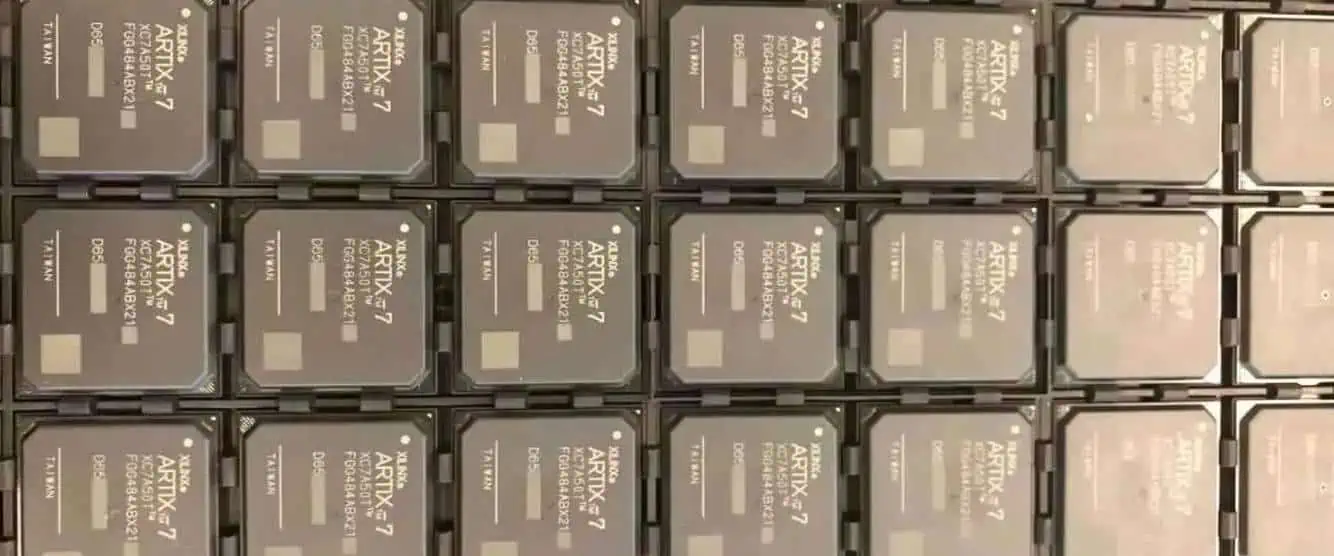
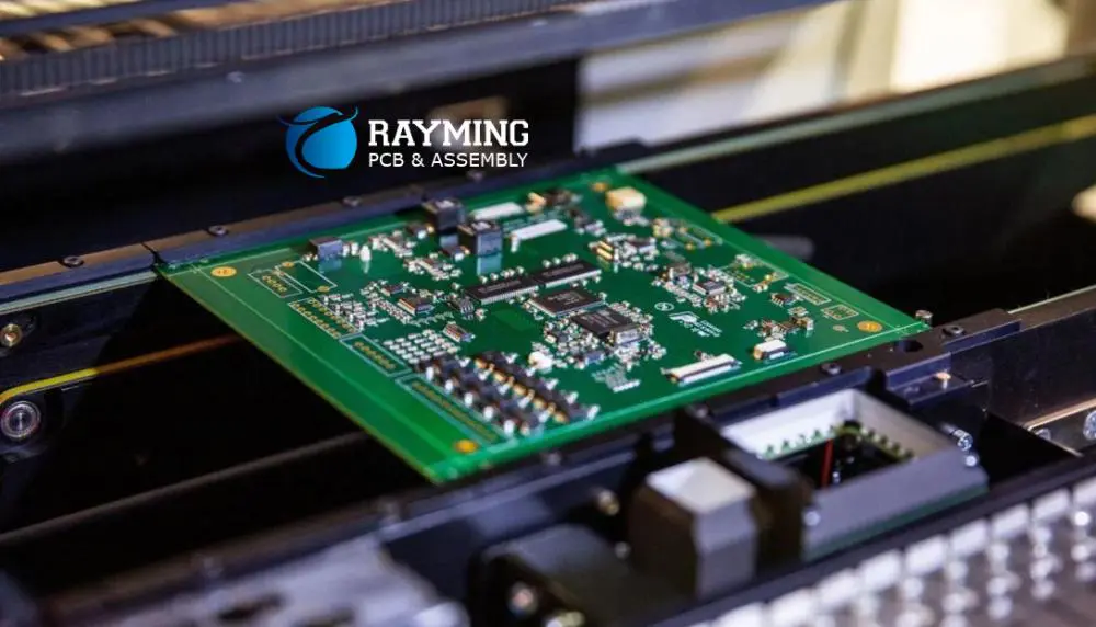
Are you searching for what is the quick turn printed circuit board? Well, it is the circuit boards that manufacturers design and manufacture rapidly in a brief period. We manufacture it in a way that it can manage demanding orders accompanied by quality products in a very short time. This article will explain its manufacturing procedure, advantages, and steps.

Introductionย 

Producers and constructors quickly produce Quick turn PCBs, as the name implies, to meet timelines. Electronic manufacturing companies avail these circuit boards not only for the quality products but also for their time-consuming and less cost quality. As you know that this I the age of electronic appliances, and with time, the demand for electronics is rising day by day, and it’s entering into the huge competition, so mass production is important. These circuits help manufacturers to produce goods in large quantities and at high standards.

What is Quick Turn in PCB manufacturing?

pcb-assembly-san-jose

You might have already heard about quick turning. But today, you will see it from a different perspective. So how do you define quick turning? It is a special method for developing PCBs. Many producers rely on quick turning because of its advantages. It maintains the PCB quality and also speeds up the production process. Quick turning involves all the steps from prototype PCB assembly to developing PCB parts and producing the PCB layers.

With this method, you can achieve all your PCB goals in a successful manner. Another great thing about quick turning is that it is an affordable method for PCB production. Therefore, no matter if you are a small PCB producer, you can go with this technique easily. It ensures consistent quality and also gets everything done at an affordable cost. However, there are some considerations that you have to keep in mind when using the quick-turning process. Always use PCB designs in the form of Gerber files. The Gerber files are reliable for safe and quick data processing and are more dependable for PCB designs when you are working with quick turning. After working on the designs, it’s time to go for the fabrication. The firm analyzes the designs, inspects them, and overviews them for the purpose of ruling out any defects in these designs. After this, the firm will decide on a quote and forward it so that the final stages of PCB production and PCB assembly can ultimately begin.

Also, if you think there is no need for prototypes for quick turning, then you are wrong. Prototypes are useful for in-depth inspection of PCBs before a producer hands them over to their clients. Prototypes also come in handy when you are producing PCBs in bulk. However, quick-turn PCBs are inevitable for stabilizing the tech-based domains and industries. These are more efficient in working and also ensure positive results.

Quick turn PCBs are also fast to produce, which means as a producer, you don’t have to invest much time in their production. Other than this, quick-turn PCBs are affordable to produce, which helps you in sticking with your production budget on all counts. All this won’t be enough when we are discussing quick-turn PCBs. Instead, we have gathered some salient reasons why you have to consider quick-turning for PCBs down below. So letโ€™s check them out right now!

Why should you consider quick turning?

  • Such PCBs are helpful in speeding up the PCB assemblies, and especially complex PCBs are easier to assemble if you follow the quick turning method.
  • You can produce Flex PCBs, which are easier to change as compared to other types of PCBs. Flex PCBs are portable, small, and have other features just because of the quick turning method.ย 
  • Quick turn PCBs are also a contributing factor for the progress and development of the telecommunication field and equipment used in this domain.ย 
  • You can even develop fast, efficient, and the latest prototypes with quick turning. It enhances their pace and also helps the producers for meeting consumer demands.
  • Quick-turn prototypes are extremely valuable for real-time inspection and detection of errors so that you can save your prototypes from the potential risk of damage and ultimate failure.ย 
  • It is an affordable method meaning the production cost is not much, which helps in bulk production always.ย 
  • The Flex PCBs developed from quick turning are heavy-duty and durable. These allow impressive heat dissipation to protect the PCBs from potential damage caused by overheating.ย 
  • It is a useful method, and it does not take much time when we are assembling the PCBs.
  • The turnaround time of PCBs is always less as compared to other methods, and it implies both flex and rigid PCBs, which is another impressive benefit of quick turning.ย 

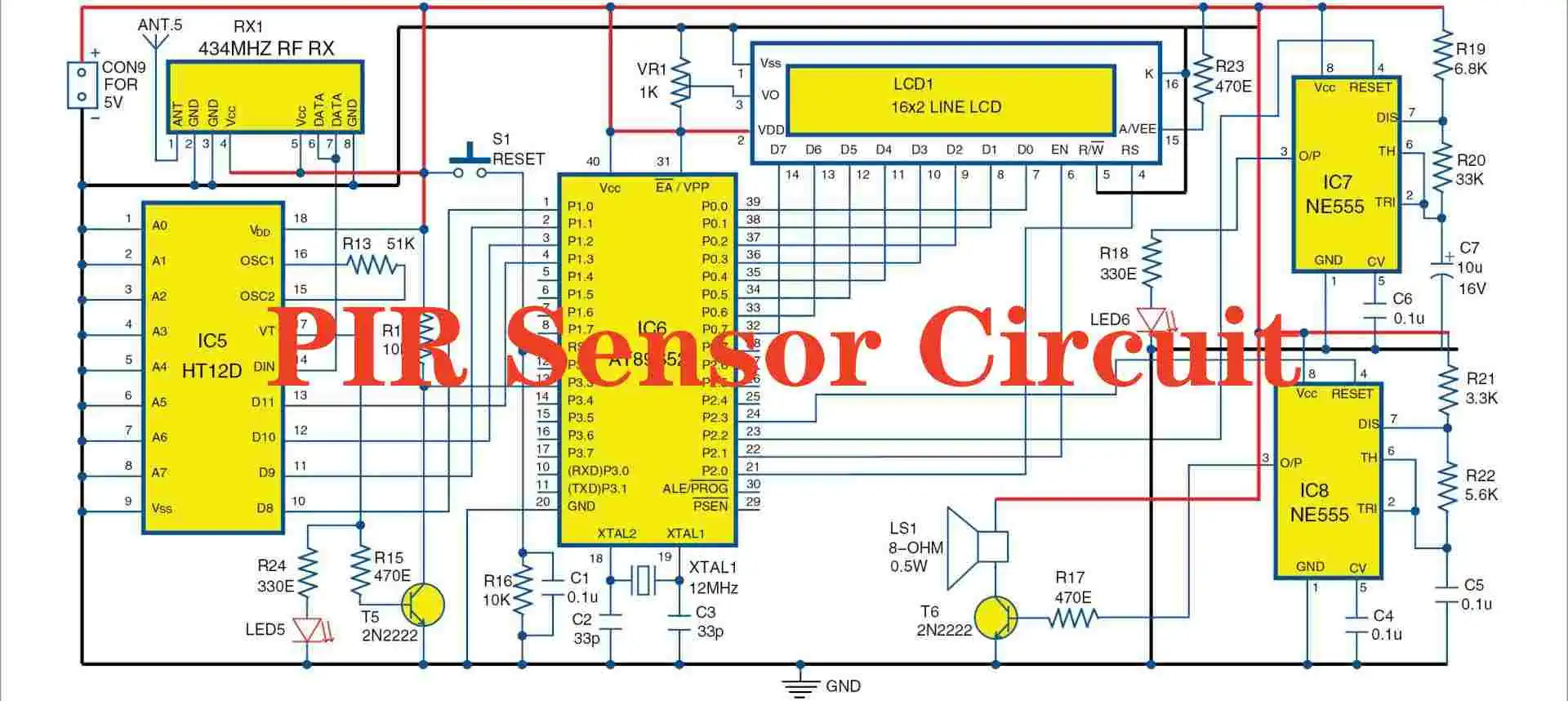
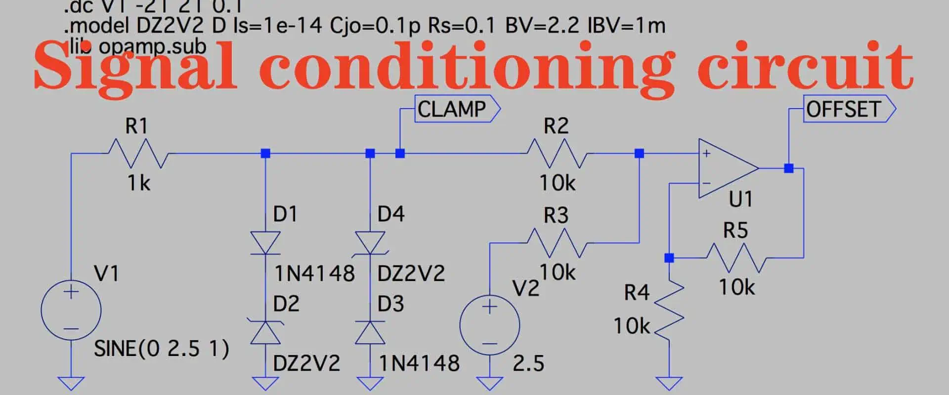
Quick Turn PCB Prototypes

ย To check the performance and potential of the circuit, we create a PCB prototype in such a way that it reaches the current applications manufactured, including the possible formalities and resources that are required from it. This help to improve the design of PCBs, providing the testing avenue and resolving any technical or regulatory issue before the start of the manufacturing process.

To make sure these PCBs are without any errors and complications, we perform corrections, addition, or omissions of features before the automation process. Prototype testing is required significant time investment in order to make sure effectiveness and performance. It is not possible to change a complete (PCB), so we can say that prototypes are crucial.

These Prototypes are beneficial because:

  • It’s cost-saving.
  • Avoid spotting manufacturing defects at the very early stage of manufacturing.
  • It saves the time of delivery by checking the manufacturability design.
  • Minimizing the changes during its production process, it also avoids manufacturing delays.
  • Based on the reviews of customers, it provides opportunities for producers to make accommodations before full production.
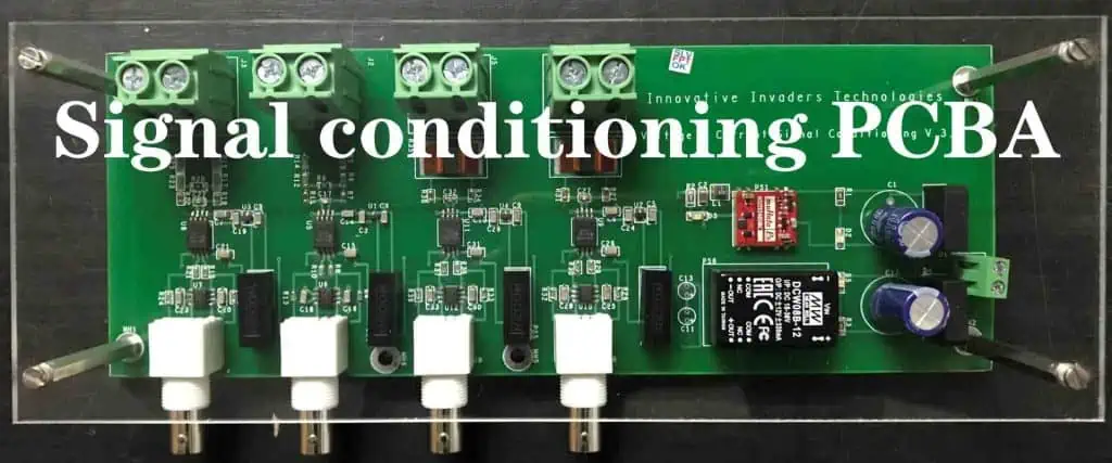
  • ย 

Pre-Production PCBs

FULL PCB MANUFACTURING Quote

Before investing considerable resources in high-volume production, these PCBs are a way to ensure production components.

It goes beyond the functionality testing that occurred during the prototyping in a way that preproduction is important for improving the gathering methods and collecting all kinds of information about manufacturing cost and time.

It is beneficial for:

  • Ensures trust and pleasure
  • Checks the arrangements of the final tooling.
  • Optimize the layout of the board for efficiency.
  • Detects faults.ย 

Full-Production PCBs

At the point where the engineering and design teams reach satisfaction point with the basic prototype. When corrections, testing, and changes have been done, at this point, full manufacturing can start. As compared to the previous stages, full production orders are larger. Companies produced large quantities of materials for the production at mass quantity production of the actual boards that will be used in devices and applications.

After the producer has done all the production steps, there is a high-quality PCB waiting for urgent delivery.ย 

Benefits of Quick Turn PCBA

When you use quick turning for your PCBs, it promises you exceptional results and more efficiency. Perhaps this much efficiency you won’t be able to get from other assembly methods. We are going to have a look at some major benefits of quick-turn PCBs here:

A time-saving advantage: PCB production is not a small process. It includes different steps which are highly crucial to develop an industrial-grade PCB. Therefore a producer invests a lot of time in this production. However, this is not the case with quick turning. It is useful when you are running short on time, and your deadlines are yet to meet. It is a good method and also saves time when you need to deliver bulk orders.ย 

Cost-saving advantage: The producers invest a lot of money in PCBs. The individual steps of the process demand a small portion of the total budget. Therefore, it is obvious that PCB production is not affordable at all. However, quick turning saves you from investing tons of money in PCB production. Quick-turn PCBs are affordable, and the entire process can be achieved within a small budget as well.ย 

Circuit board variety advantage:ย Different PCB users have different expectations of their PCBs. It means a producer has to be mentally prepared to meet the requirements of their clients. It can get difficult when you are not relying on quick turning. Quick-turn PCBs allow more room for making alterations as per your clientโ€™s demands.ย 

Applications and some more benefits of Quick turn PCBs:

  • Quick-turn PCBs are more robust than other types when the conditions are not favorable. Humidity, moisture, and heat never create a negative impact on quick-turn PCBs due to their heavy-duty and durable structure.ย 
  • The field of IoT always relies on quick-turn PCBs since these are portable and small. It means they are an integral part of telecommunications and high-frequency equipment.ย 
  • Quick turning is an incredible asset for prototyping which is why time-to-market can be minimized to a large extent. Due to this reason, quick turning is a common method used by various PCB producers. It helps them meet the customerโ€™s demands and maintain the flow in the market as well, which becomes more important than ever in some emergency cases.ย 

Disadvantages of PCB Prototyping

  • There are not many disadvantages to PCB prototyping.
  • It totally depends on you how you choose to prototype the board design.
  • While using the breadboard, most challenges arise.
  • It has many limitations, so it is not good for those who are manufacturing a complicated design.
  • It is very difficult to map your work, so it can lead to many challenges.ย 

Key Takeaways

(Quick-turn) PCB manufacturing is the best step to produce PCBs, receiving- commendations from all industries for helping in the fast increase in production with zero chance of any kind of defect. It also standardized research, design, manufacturing, and trial in order to save time and value.

Understanding the Basics of Current Sensing Circuits

current sensing circuit

The field of electronics is lifeless without current sensing circuits. Different electronics need current sensing systems for their efficient performance. Or else technical faults, short circuits, electrical fires, and complete failure can take place if there is slight negligence in current sensing.

So what exactly is a current sensor? Well, to not confuse you for this, we can define a current sensor as a mechanism for detecting the current in wiring and indicating its value no matter whether it is high or low. Now, the value given by a current sensor can be used by an ammeter for further filtering down to gain an accurate value as per the experiment or the application. The current sensors are complex and include different small circuits as well.

These sensors are available in a variety of types in the market. Different domains, like automotive, use current sensors for multiple applications. It’s time to quickly check out the principle of current sensors.

So that you can have a clear idea about how this mechanism works in major applications right from the beginning!ย ย 

Principle of Current Sensing Circuits

current sensing circuit diagram

The current sensor is not only for detecting the current. There is more to its role. It is also important for transforming the current into a voltage that has a direct relation with the current itself.

When the current flows, it will decrease the voltage along the route from which the current is flowing at the moment. The conductor that contains the current also produces a magnetic field in the system. So these are the things that you need to keep in mind while constructing a current sensor. 

Current Sensing Element or Sense resistor

Current sensing means that the system produces a voltage signal as per the current in the circuit. One common way to sense this current is to rely on a resistor and place it in the way of the current. Use a series arrangement for this so that you can keep the resistors almost anywhere in the currentโ€™s path. It means you can also call a current sensor a current-to-voltage converter.ย 

Factors affect the functions of Current Sensing Circuits

ยท Low Values to lessen power failures:

The values that you obtain from the current sensor directly relate to the threshold figure. The threshold value for such a circuit depends on the sensed data of the current. 

ยท Low-temperature coefficient:

Temperature is another factor that influences resistance. In order to maintain accuracy, you need to focus on the temperature. If a resistorโ€™s resistance is near 0, it means you can use it for your experiment. The power is also variable at different temperature ranges. However, you cannot ignore the peak power, and due to this, you need to keep monitoring the energy graph as well. 

Advantages and Disadvantages of Current Sensing Circuits

Pros:

  • Current sensing resistors are affordable
  • These offer impressive precision
  • The current ranges from low to medium
  • It can also detect AC and DC

Cons:  

  • It might interact with the resistance of the circuit flow, which can boost the output resistance leading to faulty loading.
  • Excessive power loss due to dissipation.

Procedures of Current Sensing Circuits

FULL PCB MANUFACTURING Quote

1. Direct current sensing:

  • This type of sensing follows Ohmโ€™s law.
  • You need to use a shunt resistor with a load when constructing the circuit.
  • After this, it will produce voltage through the shunt resistor.
  • This voltage will be in direct relation with the current.
  • You can use different amplifiers to determine the shuntโ€™s voltage.

2. Indirect current sensing:

  • Indirect current sensing follows Ampereโ€™s and Faradayโ€™s Laws.
  • You need a loop across the conductor that carries current.
  • It will induce voltage for the loop that directly relates to the current.
  • You can only use this indirect sensing for currents ranging from 100A to 1000A.

 You can perform indirect sensing by two more methods. These are low-side current sensing and high-side current sensing. So letโ€™s see what are the differences between their work below:

3. Low-Side Current Sensing:

  • The voltage of this type of current sensing is low in input.
  • You merge the resistors of the load and the ground together.
  • The low side current sensing is a common mode voltage which means it supports near the ground.
  • Therefore, it is reliable to use for rail-to-rail input and output for OP-AMPs if you are using any. 
  • You need to ground the resistance while the load works with the supply.
  • However, this type of sensing can interfere with the loadโ€™s functioning and potential. 

4. High Side Current Sensing:

  • It works by joining the resistors of the power supply and the loads of the circuit.
  • It is useful because it detects the current of the power supply, which helps in the prevention of the defects of a load like load shorts.
  • The input of the amplifier should have a similar range as the loadโ€™s voltage.
  • You need to ground the load after this, and you will obtain the sense current through it. 

Current Transformer (CT):

A current transformer (CT) is a device that determines a certain amount of current for you. Different producers love CT because these offer brilliant performance for the high current applications.

It has the ability to determine huge amounts of current without using much power. It is a complete power saver when it comes to its job and can be a multipurpose device for determining voltage as well.

However, it is important that you perform every step with undivided attention to prevent any chances of mishaps and complications. Or else, you can end up ruining the circuit, and it would fail to give you desired results as well. 

Summary

The range of creativity with a current sensor is limitless. You can use it as per your needs to never fall short of producing highly efficient tech electronics and the latest gadgets. Different technologies instill remarkable features in current sensors, like precision and efficiency.

We hope that this discussion rendered some interesting facts before you regarding current sensors. Now that you know how current sensors work, it’s time to give them a shot for your upcoming projects!

Understanding the Basics of Heat Sensor Circuit and Working Principle

Heat Sensor Circuit

The human body has receptors that allow it to sense heat and temperature. Similarly, machines have sensors that help them detect temperatures. So that when the temperature exceeds, it will notify the device, and the same happens when the temperature is low. Heat sensors are highly crucial for the safety and fine performance of electronics.

It is because these detect peculiar temperature changes and prevent mishaps like electrical fires and mechanical problems in the devices. If your fridge and stove are working efficiently, itโ€™s because of the temperature sensors present in their systems. We have heat sensors to talk about in this post. If you are a physics lover, you are going to enjoy learning about these sensors. So letโ€™s not keep you waiting and explore heat sensors right now!

Heat Sensor Circuit 

The heat sensors contain temperature sensors. The sensor detects temperature fluctuations when the temperature exceeds a certain limit. A LED is also present in this system, and some sensors have a buzzer as well. The phenomenon is somewhat similar to a smoke detector circuit. There are also resistance temperature sensors available.

You can also call them thermocouples. It works on electrical pulses to record temperature changes. The domain of electronics cannot survive without temperature sensors. These are working in high-end computers, home appliances, and whatnot! Such sensors are also useful to provide protection against potential damage caused by overheating. These sensors also come in handy when there is a margin to upgrade security alarms for homes and offices.ย 

Working of Heat Sensor Circuit 

LM741 Heat Sensor Circuit

The job of a temperature sensor is to efficiently monitor the temperature changes and heat fluctuations. The output voltage of these sensors greatly influences the circuitโ€™s performance. There is a diode present in the circuit which allows voltage to pass through it. So, we can infer that the resistance and temperature, in this case, are in a direct relation. Increasing the temperature means you are improving the resistance. A variable resistor can help you set the threshold if you need it for your project.ย 

Types of Heat Sensor Circuits 

The two major categories of heat sensors include:

1. Fixed temperature heat detectors

2. Rate of rising heat detectors

1. Fixed temperature Heat Sensor Circuit 

Such a sensor will contain a duo of thermocouples, and there is also a monitor present in the system. These components make heat transfer feasible through the processes of radiation and convection. The temperature changes never influence the heat detector, and it keeps performing in its natural state. If you are lucky enough to happen to determine the threshold level, you can make the sensor work even in low temperatures.

2. Rate of rising Heat Sensor Circuit 

As you know, extremely low temperatures can cause electrical fires leading to the failure of the devices. Well, if you are relying on the rate of rising heat detectors, you are on the safer side. Such sensors never support low temperatures, which are the root cause of major problems for electronics that use such sensors. It alerts you as soon as it detects unusual temperature changes. It features a special temperature element that acts up when the temperature reaches a certain limit. You will find several types of temperature sensors based on their properties. A temperature sensor is available in two types:

  • Contact temperature sensor: There must be physical contact between the object and the sensor so that it can detect solid, gaseous, and liquid through different modes of conduction.
  • Non-contact temperature sensor: It relies on modes of radiation and convection that make it able to detect gases and liquids by using IR radiation. 


Benefits of Heat Sensor Circuit 

The following are the major benefits that you get from using temperature sensors:

  • It performs its job irrespective of the medium since it has no influence on the sensor.
  • It is always quick to respond to temperature changes to save the device from electrical fires due to hot temperatures.
  • It gives output without any interference at all. 
  • It is reliable to use because of its accuracy.

Working Principle of Heat Sensor Circuit 

A temperature sensor processes the electrical signal. These sensors use some common metals that make their design efficient to work under stress conditions. These metals are responsible for producing voltage as per the temperature changes.

It also determines the voltage that moves through the diodes. When you increase the temperature, it will increase the voltage as well. 

ยท Temperature sensor circuit:

An IC Temperature Sensor has a pair of ICs in the form of temperature transducers. Now, their job is to generate current as per the temperature. The overall size of this circuit is small. It features less thermal mass and is fast with the response time, which is impressive. There is a certain range of temperatures that is optimum for this circuit to perform efficiently. 

Frequently Asked Questions

FULL PCB MANUFACTURING Quote

What Is the Definition of Heat Sensor Circuit?

A heat sensor is a type of circuit that senses heat changes by teaming up with a thermistor. Its working is similar to the changes in resistance by detecting heat. The circuit contains a buzzer, transistor, capacitor, and variable resistor in its construction. It has different applications in multiple industries. 

What are the components to design Heat Sensor Circuit?

The components important for making a temperature circuit are as follows:

  • 9V DC supply
  • Thermistor
  • Transistor
  • Relay
  • Diode
  • Variable resistor
  • 9V battery/transformer or use an adapter

What Are the Two Kinds of Heat Sensor Circuits?

You will find four versions of temperature sensors available. All these sensors have crucial applications in the electronics. These are important for ICs made of semiconductors, thermocouples, RTDs, and thermistors. 

What is the use of a Heat Sensor Circuit?

You can use a heat sensor in different electronics like refrigerators, stoves, and ACs. These are important to monitor and regulate the hot and cold temperatures of consumer electronics.

Due to this reason, temperature sensors are reliable for the efficient performance of consumer electronics and ensure their safety as well. In this way, such home appliances serve you remarkably in the long run. 

What are the Benefits and Applications of Cavity PCB?

Cavity PCB

Majority of the compact and complex multilayer circuit boards of high frequency need cavity structures in order to allow the mounting of high-power devices on heat sinks as well as mounting of sensitive devices on the ground planes.

What Does Cavity PCB Mean?

This can be described as cutouts or holes in the printed circuit board from the outer layer of copper to an inner layer of copper. However, it doesnโ€™t pass through the printed circuit board completely.

Using cavities in a circuit board for reducing the height of the component or increasing the clearances of the component is a useful as well as viable technology. Also, it can serve heat real estate constraints as well as heat requirements, just to mention a few.

The SMT testing of assembled cavity boards with BGA packages of 0.4mm at many cavity depths has revealed that printed circuit boards can be assembled, paste printed, as well as reflowed in one multilevel process successfully with the existing capability of the equipment.

Asides from keeping the mechanical design in low-profile formats, the cavity down is useful in reducing the overall thickness during the insertion of components or the design for wave guides to help reduce loss of signal and increase the transmission speed for the high frequency signals. As it does this, it also limits the transmission of signal in the slot.

What Does Plated Cavity PCB Mean?

Cavity PCB board
Cavity PCB board

A cavity can be described as any recessed opening that permits the placement of a component on layers asides from the bottom or top. This can also be described essentially as cutouts that donโ€™t find its way all through the circuit board. Though cavities could serve sophisticated and complex RF purposes, as well as aid in thermal management, cavities are commonly useful in saving physical space.

The components mounted in the recessed cavities reduce the PCBAโ€™s height effectively. The benefit of this is that this assembled board would be able to fit inside slimmer enclosures. Other cavities that are more advanced permit the complete embedding of the components. After installing the component in the cavity, other materials will be laminated over the top region, thereby sealing it inside that multilayer structure.

Placing the component in the board helps to free up space found on the external layer. This allows the placing of additional circuitry or components, or for turning the footprint of the board to become smaller.

The formation of cavities need experience with the processes of lamination as well as the selection of materials. When the layer thickness is more consistent, it becomes easy for you to control the cutโ€™s depth. It is also important to machine the cavity accurately. Due to the inevitable variations seen in the thickness of materials and the setup of the CNC machine, in addition to the copper surfaceโ€™s roughness after the mechanical milling process, it is usually necessary to substitute mechanical milling with an ablation step that is more controllable.

Construction of the Cavity PCB

The cavity PCB features structural recesses that allow extra functionality in contrast to the standard PCBs. This feature allows heat sinks to be inserted. These heat sinks are called โ€œcoinsโ€, which are useful for positioning electronic components underneath the surface. This gives your assembled printed circuit board a thinner profile overall.

Also, the surfaces of the inner cavity are also useful for electrical contacts, usually ground connection. Though there are lots of ways for creating a cavity in a printed circuit board, the method that is most common is through the removal of the material mechanically from the structure of the PCB to create a cavity in window form in the multilayer PCB.

As the prepreg and laminate materials are assembled, these layers that form the windows would create the cavityโ€™s walls. If this cavity will act as a microwave/RF resonant cavity, you determine the frequency by the cavityโ€™ size and the manufacturer of the printed circuit board must control the cavityโ€™s X, Y, and Z dimensions. Also, you can apply the designs of the cavity in many locations as well as different depths present on one PCB and can be edge plated as well

What are the Applications of the Cavity PCB Technology?

The coin and cavities technology are useful for boards that serve the following applications and industries.

What are the Benefits of Cavity PCB?

FULL PCB MANUFACTURING Quote
  • Miniaturization with the use of cavities is cost-effective in contrast to different other approaches
  • Cavities permit miniaturization in circuit board technology to rise a step further.
  • You can position cavities flexible and it can be adapted easily to new systems or components
  • With cavities, you can accommodate the components inside the inner layers; therefore it fits very complex assemblies in smaller spaces.

Creating the Cavity PCB

Devices have now become smaller, thus the PCBs space is now more precious. For a very long time, assembling outer layers hasnโ€™t been sufficient, and also its inner layers are being used.

Also, cavities ensure that components can be accommodated in its inner layers; therefore it will easily fit complex assemblies into smaller spaces. By making use of several layers, you can utilize this same areaโ€™s space to its maximum.

To be able to place the microchips, the resistors or heat sinks on recesses, circuit boards, and cavities are usually made inside the circuit boards through a laser so as to take out the desired material. First, the laser opens the surface of copper and then takes out the dielectric. Then a different laser will clean this exposed inner surface of copper from the resin residues.

Conclusion

In summary, PCB cavity can be described as a cutout in a PCB from the outer layer of copper, into the inner layer of copper. However, it doesnโ€™t pass through the circuit board completely. Using cavities in PCBs is a way of reducing the height of the component as well as increase the clearances of the component.

Why is Design for Manufacture Critical in the Electronic Product Development Cycle?

Design for Manufacture

Modern electronics are subjected to a wide range of testing processes and evaluation techniques. The design for manufacture is one of such techniques. This article explains what it is all about.

What is Design for Manufacture?

Also abbreviated to DfM, it refers to the process of engineering and modifying electronic products in a way that they follow the laid-down guidelines.

According to Wikipedia, โ€œDfM describes the process of designing and engineering a product in order to facilitate the manufacturing process in order to reduce its manufacturing costs.โ€

Basically, you can leverage the concept to ensure the quality of the product, while saving up on costs.

When to Implement Design for Manufacturability

The best time to use this technique is during the production stage of the electronic product. The following support this claim:

  • The early-stages of production are when potential loopholes are created in the productโ€™s manufacturing process. Implementing the DfM process here helps to identify these issues in real-time.
  • Once the problems and design-related issues are realized, they can be fixed in the shortest time possible.
  • It is also possible to save costs with the DfM process steps. By identifying and fixing the design issues before final production; you get to save money on dismantling the coupled product for fixture and repair.

The Core Design for Manufacturing Product Areas

The DfM process can be used in different areas of the electronic product development. The popular ones are Integrated Circuits (ICs), Printed Circuit Boards (PCBs) and CNC Machining process.

Here is a summary of how DfM can make a difference in the respective areas:

DfM for ICs

The DfM process steps are used in optimizing the performance of Integrated Circuits (ICs). The relevance here is due to the need to achieve high-yielding designs, despite the dominance of the VLSI technology.

Certain techniques are used to make the ICs โ€œmanufacturable.โ€ The cardinal points here are the reliability, functional yield and parametric field of the circuits.

Here are some of the things you need to know about the DfM techniques for ICs:

  • The techniques are used to optimize the amount of redundancy in the ICโ€™s internal memories.
  • A combination of routability, timing and power can be used to substitute the higher yield cells.
  • If permitted, the DfM techniques can be used to substitute the fault tolerant vias in a design.
  • These techniques also aid the ICโ€™s resistant, by changing both the width and spacing of the interconnect wires.

Design for Manufacturability for PCBs

Printed Circuit Boards (PCBs) also benefit from the DfM processes. Here, the design for manufacturing guidelines is used as parameters for adjudging the circuit boardโ€™s compliance with the design processes.

The following are some of the benefits in this regard:

  • DfM aids in PCBโ€™s manufacturability.
  • It also aids in the cost-saving methods. For example, it can be used to support the automation of the component placement process, rather than the hand-processing methods.
  • Design for manufacturability supports the resolution of probable production problems for PCBs.

Design for Manufacturability for CNC Machining

The primary goal of DfM for the CNC Machining process is to reduce costs. The cost-saving mechanisms are driven by the following processes:

  • It reduces the setup time for the CNC machine set-up process.
  • The process also supports the minimization of the time spent removing (machining) the materials.

The Broader Design for Manufacturability Scope

FULL PCB MANUFACTURING Quote

Different approaches can be used to actualize the manufacturability compliance of electronics and other related products. There are three (3) broader perspectives to the DfM process steps.

Design for Assembly (DfA)

This is the design-centric measures taken to ensure that the product in view is assembled properly. At the same time, the DfA process ensures the cost-effectiveness and time-efficiency of the said product.

The goals of DfA include:

  • Simplifying the component assembling process.
  • It reduces the time spent on assembling these components.
  • Labor and costs are also saved in the process. It is possible because of the use of automated processes, which reduces human inputs and in extension, saves money.

Design for Manufacturability (DfM)

Also called the design for manufacture and DfM, it focuses on how best to optimize the productโ€™s parts for the best results and to save costs.

Comparing DfA to DfM

Both Design for Assembly (DfA) and Design for Manufacturability (DfM) can be used for improving the efficiency and cost-savings of electronics.

However, they operate distinctly. Here are some of the differences between the two:

  • Design vs. Manufacturing: DfA focuses on improving the designs of the product, as a way of streamlining the component placement. On the other hand, DfM focuses on the designing and optimizing of the parts and assemblies to ensure they meet the manufacturability demands.
  • Reduction Areas: both processes deal with reduction. However, the scope of the reductions differs. For DfM, the reduction is for the number of manufacturing operations, as this helps to bolster the operational capabilities. On the other hand, the Design for Assembly (DfM) process supports the reduction of the numbers of the total numbers of parts used for the assembly.

Design for Manufacturing and Assembly (DfMA)

This refers to the combination of the Design for Manufacturability (DfMA) and Design for Assembly (DfA).

The DfMA process involves the following:

  • Process Merger: the design and production processes are merged in one package. This allows for the optimization of the productโ€™s design, while supporting the merger of the design (DfA) requirements with the production (DfM) process.
  • Integrated Product Development: for better cost-savings and to improve the productโ€™s reliability; a wide range of product development processes can be utilized.

Design for Environment (DfE)

As a holistic approach to product development, Design for Environment (DfE) has to do with the following:

  • The reduction of the environmental impacts of the product. The best results towards this regarded are derived from the reduction of the recyclability, consumption and pollution tendencies.
  • DfE goes on as long as the product is in use. Unlike the DfA and DfM processes that end after the productโ€™s assembly and production; DfE runs throughout the productโ€™s lifecycle. It starts from the raw material extraction process to the end-of-life phase of the product.

How to Develop the Best Product with the Design for Manufacture Principles

wire connector manufacturer

Certain principles must be followed to get the best results from the DfM processes. We will help you create DfM-friendly electronic products that follow these principles.

1. Select the Appropriate Manufacturing Process

The right manufacturing pathway makes the productโ€™s development easier. In the selection of the manufacturing process, you want to consider the following:

  • It is possible to use a cost-effective, yet efficient and faster variant to the productโ€™s development.
  • The overall viability of the chosen manufacturing process must also be considered. This comes in handy for the balancing of the costs with the performance. For example, the ideal production process shouldnโ€™t offer only low costs for the production and stack-up during the productโ€™s distribution.

The following parameters should help you choose the best manufacturing process for the product:

  • The post-processing needs.
  • The types of materials used.
  • Overall cost of manufacturing the product.
  • Surface finish
  • Volume: how many units of the product are to be manufactured?
  • Tolerances: the choice is to decide between the loosest and tightest tolerances. Mention must be made that the costs can add up quickly for the tighter tolerances, due to the need for secondary machining processes and the need for additional machining time. On the other hand, loose tolerances bolster easy production, cut down on the number of possible defects and reduce the design for manufacture tool costs.

2. The Product Design

How the product is designed before the actual development also impacts the design for manufacturability processes. The goal is to make the design compliant with the manufacturing principles.

Due to the complexity, the challenges and the need to make the product very design-to-manufacture-compliant; it is better off using the design for manufacture tools. These tools help to provide real-time info on the designโ€™s effects on the productโ€™s development.

Here are some of the additional details you need to know about the product design:

  • It is always necessary to juxtapose the thickness of the material before choosing one.
  • The best materials should always be used.

3. Choose the Appropriate Material

The material used for the design is as important as what the outcome would be. When making the material selection, prioritize the properties of the material, which align with what the product is all about.

The two major considerations here are the form and the overall properties of the material. For the form, the following are considered:

  • The form refers to the materialโ€™s size and shape before the machining process.
  • The product can use a variety of form, but it is important to compare the performance of one of the forms over the other.

For the materialโ€™s properties, the following are considered:

  • Flammability: this refers to the materialโ€™s exposure to burns and flames. How resistant is it to fire?
  • Mechanical Properties: this has to do with the materialโ€™s strength. However, note that certain materials might suffer reduced machinability when they become harder.
  • Electrical Properties: this lets you into the materialโ€™s acting capabilities. If it is to act as a dielectric, it means that it would be an insulator instead of a conductor.
  • Color: this has to do with the color of the material.
  • Optical Properties: this helps you determine whether the material will be transparent or reflective.
  • Thermal Properties: the material needs to have heat-dissipating capabilities. The thermal properties let you know the extent of the materialโ€™s heat resistance.

4. Exposure to the Service Environment

One of the DfM process steps is to be certain of the materialโ€™s compliance with the service environment. The properties of the product differ, based on the environment where it is subjected to.

These are a few tips on how to choose the best service environment for the product:

  • Functionality: the product should be able to function to its full capacity in the environment it is used. For example, electronic products optimized for marine applications might not operate optimally in dusty areas. The goal is to maintain a product quality that functions optimally under the normal operating conditions.
  • Environmentโ€™s Intensity: the effects and intensities of the target environment also plays a role in the productโ€™s performance. The following factors influence the intensity: abrasives, rain, moisture, snow and salt.

5. Standardized Testing and Compliance

The testing and compliance expectations must also be met, as they form a part of the basis for the productโ€™s streamlined entry into the targeted market.

The following are some of the different standards to be fulfilled:

  • Internal Standards: these are the standards set by the company and are aimed at ensuring the productโ€™s quality before it is shipped.
  • Industry Standards: these are the prevailing standards and requirements that guide the development of electronic products.
  • Third-Party Standards: this covers the standards set by the third-parties, including the regulatory agencies.

The compliance of the product to the existing standards is one way to look at it. You also want to test the product to validate the compliance before shipping. Here are some ideas on how to make the most out of it:

  • Pre-Mass Production Testing: always test the product during the design phase. This helps to prevent hiccups discovered after the entire production process is over. Testing as you design helps you to identify and fix design issues on time.
  • Vary the Test Methods: endeavor to use a variety of testing methods for the process. You may want to consider the non-destructive testing method that allows for the test equipmentโ€™s continued functionality even after the testing is completed.

Conclusion: What Does Design for Manufacture Mean?

Design for Manufacturability (DfM) is all about the designing and assembly of electronic parts, as a way of ensuring the flexibility of the manufacturing process. The benefits include a significant production cost reduction, shorter time-to-market, increased ROI, smoother manufacturing process and improvements in the productโ€™s quality.

You need to work with a DfM specialist who is good at streamlining the product development process, minimizes assembly direction, maximizes your budget and creates a modular design. RayPCB will help you do all that. Contact us today!

SOIC Vs SSOP – What are the Similarities and Differences between these IC packages?

SOIC vs SSOP

Integrated circuits are an integral part of electronic devices. These circuits are commonly found in modern devices. They are responsible for the compactness of electronic devices. Integrated circuits are the heart of most printed circuit boards. These ubiquitous black chips are available on almost every printed circuit board.

At least one IC is available in every electronics. ICs comprise a collection of components such as capacitors, diodes, transistors, etc. These components are all included in a tiny chip, which is the IC. Also, these components are connected together to help the electronic device function as expected. Integrated circuits have several types of packages. Examples of these packages include SOIC, SSOP,TSSOP, and more.

What is the SOIC Package?

SSOP
SSOP

SOIC package is a type of surface mount integrated circuit that has a rectangular body with leads protruding from two sides. The small outline integrated circuit (SOIC) package has one of the easiest SMD parts that can be soldered. Each pin on an SOIC package has a space of about 1.27mm from the next.

The leads of the SOIC package are in a gull wing shape that enables footing during PCB assembly. Due to the benefits and features of SOIC, it is one of the most commonly used SMT IC packages today. One of the benefits of this package is that it is JEDEC compliant. Also, this package is available in various body widths. The most popular body width is 3.8mm or 150 mils.

However, the standard lead pitch for SOIC package is 50 mils or 1,27mm. This IC package is usually shipped in reel and tubes. SOIC is available in various types which include the small outline J-leaded packages (SOJ), the small mini outlines package (MSOP), the shrink small outlines packages (SSOP), and the small thin outline integrated circuit package (TSOP).

These variants come with different structural measurements. However, the SOIC features 1.25mm lead spacing . SOIC is standardized and regulated in order to make installment an easy process. This IC package comes with package information that has a prefix SO. The number after the prefix is the pin count of the particular integrated circuit.

The small outline integrated circuit package is shorter than the dual inline package (DIP). It is a surface mount IC package with its DIP bins shrunk down to a smaller size. SOIC has an exposed pad which helps to improve heat dissipation more than a standard TSSOP. This helps to increase the operating parametersโ€™ margin.

What are the Advantages of the SOIC package?

SOIC offers a lot of advantages. Compared to other IC packages, SOIC provides more benefits. The most significant benefit of SOIC is the footprint reduction. This is because space reduction helps in fabricating smaller printed circuit boards. Also, SOIC minimized the cost of fabricating integrated circuits since the materials used in the packaging are reduced.

With the small outline IC package, it is easy to access small size components by a machine during PCB assembly. This IC package makes the fabrication of multilayer boards very easy since it is a surface mount IC package type. Another advantage of SOIC is that it is suitable for applications where low-cost solutions are required.

Furthermore, SOIC package makes use of at least 0.50-inch lead spacing. This helps to ensure the pins or leads have enough spacing.

Features of SOIC Package

  • It features gull wing lead configuration
  • Multilayer ceramic package
  • Comes with footprint similar to plastic SOP
  • The leads of SOIC are gold plated
  • It is a type of surface mount package with .050 inches as its lead spacing
  • SOIC is available in a few variants.
  • The pin sizes and package size of SOIC have references
  • SOIC comes with an identical pinout

SOIC Standards

The SOIC package is ideal for use in different applications. SOIC package makes use of the JEITA and JEDEC standards. However, it is quite confusing to decide which of these standards are better. JEITA is a standard set up by the Japanese trade organization to evaluate the performance of specific electronic s and the IT industries.

JEDEC, on the other hand, regulates the activities of the semiconductor market. It oversees the standardization of semiconductor part numbers and the Electrostatic Discharge (ESD) standard. The best way to differentiate between JEITA and JEDEC SOIC is the sizes. JEITA SOIC is smaller and lighter than JEDEC SOIC.

Also, the JEDEC standard is popularly used for manufacturing SOIC in the U.S while JEITA is a standard set up and used for manufacturing SOIC in Japan.

SSOP Meaning: What is SSOP Package?

FULL PCB MANUFACTURING Quote

The SSOP package is a variant of SOIC package. The shrink small-outline package, popularly known as SSOP is a smaller type of SOIC package. It integrates SMT in packaging integrated circuits. This variant of SOIC is suitable for applications where optimum performance is crucial in IC packaging that has tightened lead pitch.

The body size of SSOP is usually compressed to get a smaller version of SOIC. Also, the lead pitch of SSOP is also tightened to achieve this smaller version. The lead counts of SSOP is within the range of 8 to 64. Its body size ranges from about 209 to 300 mils. One of the benefits of this IC package is that it complies with standards like EIAJ and JEDEC.

This IC package offers a significant reduction in terms of size while providing low-cost and value-added solutions for various applications. The gull-wing leads of SSOP are extending from its longer sides. You will find SSOP in end-products like disc drivers, RDF devices or components, radio, and telecom. This compact IC packaging option comes with a lot of benefits which include improved electrical performance and better heat dissipation.

Furthermore, SSOP has solder plated leads which helps to ensure excellent performance when used in some applications.  SSOP package features leads in both sides of periphery. Also, the lead pitch of this SSOP is less than 1.0mm.

Features of SSOP

  • The tube quantity varies
  • The parts of this package are available on reel and tape according to request
  • Its body widths ranges from 209 to 300 mils
  • The copper lead frames have high conductivity
  • Also, its moisture sensitivity complies with JEDEC level 3
  • Multi-die production capability
  • The leadframe strips have higher density
  • Comes with standard JECEC package outlines

SOIC vs SSOP Package

SOIC package is a type of surface mount integrated circuit that has a rectangular body with leads protruding from two sides. The small outline integrated circuit (SOIC) package has one of the easiest SMD parts that can be soldered. Each pin on an SOIC package has a space of about 1.27mm from the next.

The SSOP package is a variant of SOIC package. The shrink small-outline package, popularly known as SSOP is a smaller type of SOIC package. It integrates SMT in packaging integrated circuits. This variant of SOIC is suitable for applications where optimum performance is crucial in IC packaging that has tightened lead pitch.

The major difference between these IC packages is in their size and the spacing between their leads.  SOIC features 1.25mm lead spacing. Each pin on an SOIC package has a space of about 1.27mm from the next. The lead pitch of this SSOP is less than 1.0mm. On the other hand, standard lead pitch for SOIC package is 50 mils or 1,27mm.

When comparing SOIC vs SSOP package, you will realize some similarities between these two packages. This is because the SSOP package is a smaller version of SOIC. Therefore, there are a few similarities these packages share. SOIC vs SSOP compares the features, advantages, and applications of these packages.

TSSOP Vs SSOP

TSSOP means thin shrink small outline package. This variant of SOIC integrates surface mount technology to package integrated circuits. TSSOP provides an efficient solution for installing ICs on PCBs. TSSOP looks like a flat rectangular IC die fixed to a lead frame encapsulated in plastic material. Also, the lead frame comprises elongated pins or leads arrange along a packageโ€™s perimeter.

From its name, TSSOP is a thin variant of SOIC. The thin profile of this IC package enables greater density on a circuit board. Furthermore, TSSOP is more compact and thinner than other IC packages or SOIC variants. Due to the space-saving feature of TSSOP, this IC package is an ideal option for applications where functionality and high level integration is needed in a limited space.

Although the SSOP package is a variant of SOIC package, TSSOP is more compact than it. The shrink small-outline package, popularly known as SSOP is a smaller type of SOIC package. It integrates SMT in packaging integrated circuits. This variant of SOIC is suitable for applications where optimum performance is crucial in IC packaging that has tightened lead pitch.

Asides from the compactness TSSOP package offers, this package option provides enhanced heat dissipation when compared to SSOP. Furthermore, TSSOP offers excellent electrical performance due to the close spacing between the leads and the IC die. Therefore, this enables reduced parasitic and shorter signal paths.

This IC package offers a significant reduction in terms of size while providing low-cost and value-added solutions for various applications. The gull-wing leads of SSOP are extending from its longer sides. TSSOP provides a wide range of benefits which include increased reliability when used in electronic devices.

Both TSSOP and SSOP packaging are popular IC package options for different applications in the electronics industry.

What are the Applications of TSSOP?

TSSOP is an alternative option when SSOP is not suitable. The thin shrink small outline package is widely integrated in various electronic devices. Due to its compactness and excellent electrical performance, it has become a popular IC package option among electronics manufacturers.

TSSOP package is commonly used in microcontrollers. Microcontrollers are used in various devices like medical equipment and industrial machines. Since TSSOP is very thin, it is ideal for microcontrollers. Also, this package is great for various electronic devices like power management ICs and memory modules. Since these devices need great functionality and high level of performance within a limited space, you can consider TSSOP package.

Over time, TSSOP has found its use in several electronic applications. Also, you can find this packaging in different markets and industries like consumer electronics, automotive, and telecommunications among others.

Other SMT Packages

Asides from SOIC packages, there are also other SMT packages. These days, there are various surface mount IC packages. You need a custom PCB to work with these packages. This PCB must have a matching pattern of copper for soldering. Below are some SMT IC packages.

Quad flat packages

A quad flat package has IC pins in all its four directions. These pins are about 8 per each side of the package. The pins of this package have a spacing from about 0.4mm to 1mm. There are smaller variants of the quad flat package. This include low-profile packages (LQFP), thin quad flat package (TQFP), and very thin quad flat package (VTQFP).

Quad flat no-leads (QFN) package

You can achieve a quad-flat no leads (QFN) package if the legs of a QFP are sanded off. QFN packages have tiny connections and there are exposed pads. Sometimes these pads are exposed on the bottom and both sides. The other package exposes the pad on the chipโ€™s bottom. Also, the QFN package has smaller variants which are TQFN, micro lead (MLF), and VQFN. There are thin-dual no-lead (TDFN) packages and dual no-lead (DFN) packages.

Conclusion

SOIC packaging has several variants which include TSSOP, SOIC, MSOP, and SOJ. We have discussed SOIC and TSSOP in this article. These IC packages are some of the most popular IC package options. SOIC packaging and its variants integrate the surface mount technology to package ICs. These IC packaging options offers unique benefits.

Due to the benefits of these IC packages, they are considered a great option for various electronic devices. Also, they are used in different industries like telecommunications and automotive.

What do you need to know about PIR Sensor?

PIR Sensor Circuit

PIR sensors play vital roles in modern daily life. No one can imagine starting without them, as they are present in almost all modern devices because of their amazing features, which include consistency, easy usage, and cost-efficient.

These sensors are mainly used in security alarms. Door openings, lift lobbies, vending machines, auto light switches, and much more. Moreover, as these sensors give a variety of benefits, it also takes part in projects like Arduino and Raspberry. This article, however, tells you about PIR sensors, their usage, applications, and working principles. 

What Is PIR Sensor?

Passive Infrared or PIR sensor refers to a type of sensor that helps in measuring the light of infrared radiation coming from objects such as animals or the human body. PIR sensor has the ability to detect or identify human or animal movement in a specified range. Typically, every object that has a body temperature above zero produces heat in the form of IR radiation. Therefore, the higher the temperature of the object, the greater the radiation. Moreover, the human eye cannot see or observe these radiations because of theIR wavelength it emits. Thus, PIR sensors are basically made to detect and sense these types of infrared radiation. It usually uses in motion sensor devices, auto light switches, and security alarms.

Working Principle of PIR Sensor

PIR Sensor
PIR Sensor

The PIR sensor contains two basic components. This includes a fresnel lens and pyroelectric sensor. The sensor comes in a circular metal form which contains a crystal in a rectangular form right in the middle of it.

However, the fresnel sense refers to a type of lens that identifies the infrared signals through a pyroelectric sensor. Moreover, a pyroelectric sensor can detect various levels of infrared radiation.

The Pyroelectric Sensor

A pyroelectric sensor contains a window with two slots in a rectangular form. Moreover, it comprises silicon coating, which allows the infrared radiation to flow simply. Then, it has two separate electrodes of the Infrared sensor. In both of these electrodes, one produces positive output while the other produces negative output. 

However, when the movement in the sensor region stops, then both rectangular slots identify similar Infrared radiation, which gives zero positive output signal. Even when the body of an animal or human moves in a sensor region, it just interrupts half of the sensor first. Thus causing a positive change between the two parts. However, when the body moves through the other half, it generates the opposite result, a negative output signal. The changes between the voltages detect the motion.

Fresnel Lens

A Fresnel lens basically enhances the field and capacity of view of sensors. It contains the capacity to gather light as well as being compact and lightweight. Hence making the size of the sensor small yet powerful.

When the body of an animal or human enters the sensor detecting range, the sensor automatically starts getting the IR wavelength of the light from the object. When it detects the infrared waves, it automatically turns on the light. However, when a body does not pass through the range, the sensor cannot sense any wave and automatically turns off the light. So a type of sensor that senses waves and switches lights is called a Passive IR sensor light. Moreover, if an object or body remains in the detecting place, the light also stays on constantly. But as the body or object leaves the detecting place, the delay automatically turns off the light.

Specification & Characteristics of PIR Sensor

PIR sensors offer various types of specifications and features. Some of them include voltage supply input and output. The input must range from +5 Volts, while the output voltage must range to 3.3 volts. It does not detect the human or object but also differentiates between them properly. Moreover, it contains both non-repeatable and repeatable operation modes. The drain of the current must stay above 60uA while the angle of detection must stay above 140 degrees. At the same time, it offers a distance of detection ranging from 7 to 3m. It contains a 2.5s blockade time default. Lower utilization of power must range 65mA while working temperature between+80 -20ยฐC. 

Different Types of PIR Sensors

Passive Infrared sensors have two types. These types include;

ยท Thermal Infrared Sensor

Pyroelectric IR sensor or Thermal IR sensor uses thermal sources such as infrared, which helps in detecting objects. These sensors process slowly and give slow detection and response time.

ยท Quantum Infrared Sensor

Quantum IR refers to a type of sensor that detects or identifies photos present over the wavelength. However, these photons respond more quickly than detecting heat. This type of sensor operates efficiently and has fast detection and response time. Though, it requires a proper and constant cooling mechanism to measure the exact location.

Circuit Diagram Explanation of PIR Sensor

PIR sensor proves ideal for installing in security systems. It offers features like robustness and low cost, which makes it perfect to use in the design of security circuits. The PIR sensor supports the circuit to make a motion detector device along with a relay.

This relay turns on the light as the motion detector senses any human movement. Motion detector PIR circuit requires a few basic components to make. This includes a PIR sensor, A relay of 5 V, a BC547 transistor, a 1N4007 diode, a 1k Ohm resistor, an electric bulb, and a 9 V battery.

Major Applications Of PIR Sensor

FULL PCB MANUFACTURING Quote

Passive Infrared sensors are used in a variety of applications and devices in distinct fields. These fields include a lift lobby, outdoor light automatic switching, and covered parking lots. Moreover, it also uses automatic switches for garden lights which work on the human presence. Also it is used in automatic doors of shopping malls which also works on sensing a human presence. Here are two basic yet innovative design projects of PIr sensors. 

ยท Automatic Door Opening System

The latest, innovative automatic door system uses a PIR sensor to operate. When a human goes through an automatic door, the sensor produces output pulses.

However, these pulses go to a microcontroller. This microcontroller controls and manages the motor driver. It accepts the input pulses and enables the motor driver to work appropriately.

ยท Security Alarm System

Banks and big companies that need utter safety of their assets use security systems. These systems use PIR sensors to work. The circuit contains IC UM3561. It refers to a type of integrated circuit.

This special IC takes input in digital signals and produces multi tones for the alarm like police, ambulance, and fire brigade sirens. Like other sensors, it detects the presence of humans as one passes through it, and it gives output in digital form. This output goes to the IC UM3561, which produces the desired siren.

The Ultimate Guide to Signal Conditioning Circuit

signal conditioning circuit

The process in which we collect the data with the help of a signal conditioner is known as signal conditioning. This device will convert the input mechanical signal into another form known as an output signal.

We do this so that we will convert difficult data into easy data which a user can read easily.

We use this device because it is more convenient than human working as it is more accurate in calculations.

It converts hard reading of data into simplest ones. Not only this but this signal conditioner also does many other useful functions which are not easy for humans to do in less time. We humans are more efficient than machines, but still, we made some mistakes that make us less efficient than machines in some aspects.

Now we will discuss the structure of the signal conditioner :

The signal conditioner will convert the input mechanical signal into another form known as an output signal. We do this so that we will convert difficult data into easy data which a user can read easily. In all of its functioning, signals plays an important role as it converts from mechanical to other type of signals, which are readable and easy to monitor.

The signal conditioner has different types, which depend on the physical value as well as on specific features.

Types of Signal Conditioning Circuit 

Signal conditioning PCBA

ยท Temperature Signal Conditioning Circuit 

There is some kind of conditioners that are responsible for measuring temperature of different ranges; they are known as temperature conditioner. They are used in the fields where we have to deal with sensors and deals with other aspects. After examining these, we will transfer signals ahead for further examination.

ยท Thermocouples

Thermocouples are another type of conditioner, as they are most common in industries in building applications. The output of the thermocouples is nearly to +ve or -ve 80 million volts. This is such a small amount of voltage which is difficult to monitor and display as they are weak. Signals with more temperature are easy to manage and display.

Signal conditioning is important not only for making signals stronger but also for fixing temperature measurement mistakes caused by something called “cold junctions.” You see, when we connect a thermometer thingy called a thermocouple to a measuring device, there’s a voltage that shows up at these junctions, and they’re cold, hence the name. These cold connections mess up the real temperature readings and give us wrong results. But fear not! Temperature signal conditioners come to the rescue. They fix these variations and make sure we get accurate temperatures. They’re like the superheroes of thermometry, saving us from bad measurements and keeping things cool. Now that’s what I call a hot topic!

ยท Thermistors Signal Conditioning Circuit 

So, there’s this thing called a thermistor, and it’s a fancy temperature sensor used in all sorts of industrial stuff. But here’s the deal: this sensor needs some special treatment to work properly that requires current and voltage. The way we give it this attention affects how stable and accurately it works.

Now, temperature signal conditioners step in as the cool cats take care of thermistors. They not only give them a boost but also help them chill out (low pass filtering), making them super easy for digital devices to understand. 

These signal conditioners are like the backstage crew for thermistors, making sure they shine bright on the temperature measurement stage. They’re the heroes that make sure things go smoothly. So next time you see a thermistor, say, “Thanks for being cool, little temperature detective!”

Functions of a Signal Conditioning Circuit 

FULL PCB MANUFACTURING Quote

ยท Signal Conversion

The signal conditioner will convert the input mechanical signal into another form known as an output signal. We do this so that we will convert difficult data into easy data which a user can read easily.

In all of its functioning, signals plays an important role as it converts from mechanical to other type of signals, which are readable and easy to monitor. It can convert any kind of signal into another form of it as we discuss it earliest.

ยท Linearization

This is a process in which a conditioner performs a function where the sensors will not catch a straight line with the help of a physical medium.

In it, it will catch signals from the software and convert them into another form of signal. Letโ€™s be honest. We all want a correct and accurate result, and by using this process known as linearization, we can get desired output.

ยท Amplifying

After linearization, we have another step amplifying, as it is a multi-stepped process. It will work under two major points

  1. We will increase the frequency of the signals which we are taking as an input.
  2. The option is that we can increase the ratio of signal to noise.

There are other types of signals known as Dc input signals, and for many other purposes, conditioner uses amplifiers of different ranges.

ยท Filtering

Listen up, folks! Signal conditioners have this function called filtering, and it’s all about cleaning up the signal’s frequency party. We want to keep the good stuff and kick out the noisy stuff. As we all know, it is the most important part of filtering.

  1. Now, there are different types of filters, and they can be built with weird components. Passive filters are like a small thing, using stuff like capacitors, resistors, and inductors. They keep the gain (volume) at a max of one, so no one gets too loud.
  2. On the other hand, active filters are like the life of the party! They mix passive components with active ones, like operational amplifiers and transistors. 

Remember, filtering is the way to keep the signal accurate and noise-free. As it is the most important part of the filtration.

Evaluation and Smart-functions

To get more benefits from it, we modify the signal conditioner into a modern conditioner having more advanced features in it. This can include weird alarms and different sounds. We modify this so that we will get advanced features.

ยท Interfaces

Ok, so, like, signal converters help send signals to machines. They can do it in two ways – analog or digital. Analog signals are like +/- ten V or +/- twenty mA, which is pretty simple to handle, but each one needs its wire. And they can even transmit extra info, like when your sensors are feeling sad or sick or whatever. It’s like a doctor for machines. But overall the wires play an important role in it. The different information on different parts of the machines is very important as it helps in the maintenance of the machine.

A Closer Look at FCBGA: Flip Chip Ball Grid Array

Flip Chip

You might be doing the flip-chip method all wrong this whole time! The purpose of a flip chip is to reduce the connections between the chips themselves. One thing that eases the purpose of the flip chip is the solder joints. 

You only need to put these solder bumps on the upper surface of the pads. The first step of the process is to use and place circuits on the semiconductors. After that, you need to position the pads and place the solder carefully on individual pads. 

Now it’s time to cut the chips and flip them all. It will assist you in placing the solder on the pads as well. In the end, you need a reflow method for the solder that solidifies its bonds with all the pads.

We know that all this must be too overwhelming for you to read straight in the introduction. No worries, since this post is going to render you all the necessary information about the flip-chip method in a fun and insightful way. 

Letโ€™s get started with this fun ride without wasting any instants!

Common Flip Chip Ball Grid Array Packages

Wait, did you not know about common flip packages? Well, these are important to have a look at in order to understand this whole process. These are made from ceramic substrates, and you can use natural laminate for these as well.

 The flip-chip wafers give you an edge since you can use two metallic layers to group them or assemble them in as many layers as you want. 

Why Use a Flip Chip Ball Grid Array?

Now that we are discussing the flip chip in detail. Have you ever wondered why they even matter in the first place? Sit back and relax since this section is going to shed some light on the major benefits of using a flip chip BGA for you:

These are reliable for intense machinery and high-frequency tools.

Flip chip BGA is always small and takes less space on the wafer, which makes it dependable for regulating inductance and increasing the transmission of signals.

The flip chip prevents moisture from taking over your wafer as well.

It allows more thermal conductivity to take place. 

The flip chip process is more practical to use instead of the regular wire bonding technique.

The flip-chip BGA method is a cost-effective technique that all producers can perform.

The flip chip is highly inevitable for the fine performance of common semiconductors used today.

Drawbacks of the Flip Chip Ball Grid Array

It’s time that we leave no stone unturned in providing you with an unbiased review on flip-chip BGA. Hereโ€™s the thing, the flip chip does have several benefits to offer. But you cannot use this method blindly. There have been cases when the recklessness of the producers in using flip chips caused them irreversible trouble. So the common drawbacks of the flip chip method that you need to know are:

They are carrier-less which means you cannot always replace them easily when needed

Due to no carrier, these are not suitable if you are trying to install them on your own (manually)

You need highly flat surfaces to combine flip chips for efficient performance 

The flat surface needs to be maintained for temperature regulation which is not always easy to achieve 

Factors affecting the Flip Chip Ball Grid Array methods: 

Now you know about the common disadvantages of flip chips. There are some factors that you need to take care of while working with flip chips. These are:

Keep the surface as flat as possible

Maintain optimum temperature on the flat surface

Control thermal expansion as it can develop cracks in wafer

Use suitable flip chips right from the start because they don’t allow easy replacement

Market Overview of Flip Chip Ball Grid Array

The connections that develop among flip chips are collapse connections. It is a process that joins the semiconductors and integrated components to the circuits that are on the outer side. All this happens with the help of industrial-grade solder bumps that you need to accurately place on the pads. If you ask for one thing that acts as a fundamental block to make it all function is the solder bumps.

Without these, no wafer can get the benefits of flip chips at all. You need to integrate the circuit on the wafers before proceeding with the process. One chip contains a pad and a solder ball of its own. After cutting the chips, it’s time that you face them toward the external circuit. All that remains is to reflow the solder to harden the bond between the solder and the setup.

Market Dynamics

FULL PCB MANUFACTURING Quote

High-performance Flip Chip Ball Grid Array

The semiconductors need to offer precise electrical performance, or else they will not meet your expectations at all. As you know, BGA always has small connections among its components. It means it reduces the resistance of these connections at the same time. Due to this, it boosts the electrical performance. Now, if you are successful in increasing the electrical performance, it will automatically improve the signal transmission and signal speed. 

Miniaturization

FCBGA impresses producers due to its irresistible benefits. It is now more important than ever for producing small and midrange consumer electronics. Wearables and mobile phones cannot work in a natural state without this method. Not only this, but CPUs also start performing better due to the excellent miniaturization offered by FCBGA. 

Improved signal integrity

You will find this interesting. FCBGA maintains the connections of IC and PCBs that give birth to short signal routes. If a signal route is short, it will prevent the disturbances as well. Signal disturbance mostly happens when there is too much noise at the backend. The solder amount used by this technique is less, which is beneficial for preventing signal fluctuations. 

Market Restraints of Flip Chip Ball Grid Array

Expensive Packaging

You might be hurt to know this, but FCBGA is not affordable at all. Only giants of the industry can think about using this method for efficiency. Several steps of this process require an individual budget that definitely is important to consider in case you need to save your business from bankruptcy. 

High Cost

The FCBGA sector is already facing enough problems since analyzing and manufacturing wafers through this method is expensive. It is a high-cost deal that hampers other processes as well. There are some other technologies, like metallization and lithography, that increase the cost of FCBGA. 

Competition

The FCBGA sector has now become ever-competitive. There is an extreme sense of remaining ahead of each other among business rivals. It is healthy, but just to some extent. Such a throat-cutting competition can create a negative impact on the buddy companies that are just stepping into this field. 

Market Opportunity for Flip Chip Ball Grid Array

Enhancing Performance

You can rely on FCBGA since it produces highly efficient semiconductors. The role of these chips is to make sure that the devices perform the best possible in the long run for the users. Due to this reason, these are useful for extreme and intense applications like super-computing operations, complex data processing, gaming, and much more

Personalization

Customization is another factor that gives FCBGA an edge over the others. It is because this produces mostly small and portable devices that are easy to change and personalize. 

Factors driving the development of the Flip Chip Ball Grid Array market

 The growing attraction of miniaturization is one of the primary factors that is contributing to the expansion of the FCBGA sector. Not only this, IoT and its vast applications in the lives of consumers are also drawing the attention of investors in the market. 

Key trends in the Flip Chip Ball Grid Array market

 Some enticing trends that are important for setting a direction for the FCBGA domain are:

The growing need for HDI that promises more miniaturization

Significance of industrial-grade materials

Solutions for thermal regulation

Applications of FCBGA in the field of 5G infrastructure

XC6SLX16-2FTG256I FPGA vs. Traditional Microcontrollers: Which One is Right for Your Project?

Xilinx Artix 7

Technology and electronics are constantly evolving. As a result, you have access to a wide range of innovative applications. A few years back, it was a microcontroller that revolutionized the world, but nowadays, FPGS is making the buzz. Both are useful in electronic projects. Field-programmable gate arrays and microcontrollers are both different. If you need clarification on using an XC6SLX16-2FTG256I FPGA or traditional microcontrollers for your project, then you don’t need to worry. The following content will help you decide which one is better.

Our vote is in favor of FPGA XC6SLX16-2FTG256I, but we will let you decide. The following content will help you understand the differences between these too. It will also help you to make an informed decision about which one is perfect for your project. That’s why it is necessary to know the basic difference between these two.

 What Are Microcontrollers and FPGAs?

 Before we dive into the differences between microcontrollers and XC6SLX16-2FTG256I FPGA FPGAs, let’s first define what they are.

 What Are Microcontrollers?

ย A microcontroller is a small computer on a single IC. It can control various devices in electronic projects. They are pre-programmed with specific instructions. They can perform several useful tasks, such as reading sensors and controlling motors. It can send data to other devices, but its compatibility is an issue sometimes.

What Is XC6SLX16-2FTG256I FPGA?

 XC6SLX16-2FTG256I FPGA FPGAs, on the other hand, are programmable logic devices. That allows users to design their own digital circuits. These are not pre-programmed, but rather you can program and reprogram them. If you particularly talk about the XC6SLX16-2FTG256I. It is manufactured by Xilinx. It belongs to the Spartan-6 family of FPGAs. This FPGA has 16,640 logic cells for better function. It has an amazing 576 KB of RAM and 20 DSP slices. It operates at a maximum speed of 400MHz. The FPGA is also so amazing because it has a range of I/O interfaces and Ethernet. That’s why it is suitable for a variety of applications, such as high-speed communication and image and video processing. This FPGA is also suitable for digital signal processing. As a result, you can achieve your electronic objectives so easily.

Differences Between Microcontrollers And XC6SLX16-2FTG256I FPGA

 Now you have a basic understanding of what microcontrollers and FPGAs are.  Letโ€™s dive into depth to know the differences between the two.

1. Flexibility For Programming

One of the key differences between the microcontroller and XC6SLX16-2FTG256I FPGA FPGs is their flexibility. Microcontrollers are not flexible in terms of programming. It is pre-programmed with specific instructions. That’s why they can only perform tasks that they have been programmed to do. On the other hand, FPGAs are able to perform a wide range of tasks, making them much more flexible than microcontrollers. Reprogramming is easy for XC6SLX16-2FTG256I FPGA FPGs, as compared to the microcontroller.

2. Processing Speed Matters

 Another important difference between microcontrollers and XC6SLX16-2FTG256I FPGA FPGs is their processing speed. Microcontrollers have a downside in matters of processing speed. They take time to take instructions and process them. In short, all microcontrollers typically have a lower processing power than FPGAs. It means that they may struggle to perform more complex tasks. XC6SLX16-2FTG256I FPGA FPGs have a higher processing power with an amazing 576 KB of RAM and 20 DSP slices. That’s why it can handle more complex tasks with ease. So again, FPGA wins the race.

3. Development Time And Customization

ย The development time is again different for both microcontrollers and FPGAs. Microcontrollers are pre-programmed. That’s why they require less development time. XC6SLX16-2FTG256I FPGA FPGAs require more development time. Users program it according to their needs. Again there is another thing: customization. You cannot customize the microcontroller. They are programmed with specified instructions and programs. That’s why they perform specific tasks.

However, XC6SLX16-2FTG256I FPGA offers greater flexibility than microcontrollers. That’s why you can easily customize them. Many designers compromise developmental time due to customization. Customization allows you to make you. The XC6SLX16-2FTG256I FPGA is more unique and suitable.

4. Power Consumption and Management

Designers and engineers always try hard to maximize efficiency and want to consume less power. Power consumption is another discriminating factor. It will help you decide your cup of tea.

 Some microcontrollers typically consume lower power while some consume more. It depends upon their programming and the specific task they can perform. On the other hand, every FPGA consumes less power especially. XC6SLX16-2FTG256I FPGA. So you can compare the power consumption of both for a particular project. As a result, you can choose which suits your needs. It is also possible thatXC6SLX16-2FTG256I FPGA is consuming more power when you compare it with your selected microcontroller. So power consumption is another important decision factor.

5. Price Difference

ย Price is also an important factor to consider but not that much. ย In my opinion consider the cost as the last deciding factor. If you are a hobbyist, then you must consider it. Microcontrollers are generally less expensive than. XC6SLX16-2FTG256I FPGA. That’s why if you are working on a tight budget, then go for the microcontroller. FPGAs are at a higher cost. But they can integrate into systems seamlessly. However, it’s important to note that the cost of FPGAs has been decreasing in recent years/on the other hand; its popularity is also increasing. Most designers consider it a more viable option for some projects.

Wrapping Up Things

I hope now you have a better understanding of both microcontroller and your technical requirements also matter a lot. Nowadays, devices and machines are more sophisticated, so an FPGA can fulfill your needs best. However, sometimes microcontrollers are the economical solution. That’s why it is up to you which option you go.

But nowadays, most modern applications use the XC6SLX16-2FTG256I FPGA due to its unique features. That’s why an FPGA is more sophisticated than any microcontroller. So go for any one of them by keeping your needs in mind. Above all, if you find yourself confused, you can seek professional or expert help.