Everything you need to know about Keypad PCB

keypad PCB

If you are an engineer, gamer, or hardware enthusiast, you have probably heard of or come into contact with a keypad-printed circuit board. However, these keypad PCBs often present themselves in a manner that makes them feel and look like complex components. Therefore, most people in the tech industry usually prefer to purchase ready-made keypads instead of producing their own. But what if there was a way to produce your keypad-printed circuit board?

A keyboard-printed circuit board sets aside the mechanical keypad from a regular keypad. Therefore, no matter the type of keypad you are planning to generate, a traditional membrane or mechanical keypad, you’ll need in-depth knowledge of the different kinds of keypad printed circuit boards. Moreover, you should be able to answer simple questions such as, what is a keypad PCB? What is the difference between traditional membrane keypads and mechanical keypads? And so much more.

What is a Keypad?

keypad board
keypad board

Keypads are generally sets of keys or buttons bearing digits, alphabetical letters, and/or symbols placed in perfect order on a simple pad. These components are usually utilized as input devices on various gadgets, which include personal computers or PCs.

Keypads can bear numeric digits exclusively; for example, keypads found in calculators or digital doors. Moreover, they can also bear alphanumeric values, for instance, the keypads on various cellular phones.

Desktop computers mostly come with keyboards with various keys that users utilize to input data onto a computer. For instance, a standard desktop computer keyboard comes with two variations of input keys for numerical digits:

  • One variation is found on the upper part of the keyboard in row-form
  • The second variation is on the right portion of the keyboard, and it tends to be more efficient in terms of data entry

However, for more compact computers, for example, notebooks and laptops, users sometimes have to insert external plug-in keypads to gain all the features that come with the standard desktop keyboard.

Keypad Printed Circuit Boards in a Nutshell

A keypad-printed circuit board is basically a sheet or a panel in a PC that acts like the keypad’s foundation or main component. Typically a keypad printed circuit board senses and defines whatever happens when users press keys in a keypad.

Using a keypad-printed circuit board, you can easily determine the key that was pressed on the computer. Moreover, you can also transfer information to your PC using the keypad in a matter of seconds.

A keypad has two main parts, which are the following:

  • The physical keys โ€“ these are the keys that the users see
  • The controller part โ€“ this is the part that carries out all the processing. Unfortunately, it is usually in the background; therefore, users can’t see it while using the keypad.

Most technicians use thin plastic sheets and metal or epoxy components to generate keypad circuit boards.

Main Differences between membrane and Mechanical Keypads

FULL PCB MANUFACTURING Quote

Membrane and mechanical keypads have multiple differences, which include the following:

Size and Cost

Membrane keypads, which also go by the name traditional keypads, are generally light and affordable. On the other hand, mechanical keypads are bulky and expensive.

However, even though membrane keypads are affordable and lightweight, they tend to have a shorter life span when compared to mechanical keypads.

Operation

Membrane keypads have rubber underneath. Therefore, you get a mushy feel whenever you press a key when using this type of keypad. Moreover, this rubber feature makes these keypads relatively silent. On the other hand, mechanical keypads have spring-loaded switches beneath the keypads that effectively trigger whenever you press a key. As a result, mechanical keypads tend to respond with pretty loud clicking sounds.

Feedback

Due to the design of the mechanical keypad, it provides more efficient feedback compared to the membrane keypad.

Rollover

Mechanical keypads tend to have a vital feature known as rollover which helps them spot essential key presses simultaneously. Due to this feature, the mechanical keypad tends to be great in the following:

  • Fast typing
  • Playing games
  • Crouch jumping and much more

On the other hand, the membrane keypad lacks this crucial rollover feature. Therefore, these keypads tend to lag your input due to limited processing.

Pressing Power

When using a mechanical keypad, you don’t have to apply much pressure to the keys to input data. By gently clicking on the keypad keys, the board’s mechanism automatically detects the keystroke and registers it into the processing unit. However, when working with a membrane keypad, you must apply a lot of pressure on the keys to register the keystroke. That is because the rubber layers on the membrane keypad must touch the circuit for the data to be submitted effectively.

Customization

Mechanical keypads are super easy to customize, unlike membrane keypads which require a lot of effort and time.

How can you generate a Custom Mechanical Keypad?

In this section, we will effectively discuss all the steps you must follow to generate a custom mechanical keypad.

First, you’ll have to gather various components you will use on your mechanical keypad. These components include:

  • A printed circuit board
  • USB cable
  • Keycaps
  • Case and back plate
  • Keypad switches
  • Stabilizers

Combining the Parts

To combine all the parts and generate a functional keypad, you should follow the following steps:

  • First, check whether or not the keypad printed circuit board is working.
  • Next, carefully mount the keypadโ€™s cherry stabilizer on the circuit board.
  • After attaching the keypad’s switch to the circuit board, flip the printed circuit board over and solder the components.
  • When the soldering process is over, you must connect the keycaps.
  • Once you are done mounting the keycaps, you can move on to the testing phase, which involves testing the keypad to ensure it is functioning according to your specifications.

To test the keypad, connect it to your PC using the USB port, then check whether the keys function accordingly.

Conclusion

Keypads are vital components in any desktop, laptop, or simply any computer setup. Without a keypad, users can’t be able to input critical information into a computer. Moreover, the entire industry shifted since keypad-printed circuit boards hit the market. These components basically make keypads more efficient compared to traditional membrane keypads. Therefore, if you want to try out keypad-printed circuit boards, we hope this article has helped you with all the information you were looking for regarding keypad PCBs.

How Toย Order PCB with componentsย in the Right Way?

The contents of this repository comprise all the necessary files for the production and assembly of b-parasites. Typically, the fabrication process involves placing an order with a company capable of manufacturing the PCB and performing surface mount technology (SMT) assembly, which consists of mounting various components such as capacitors, resistors & oscillators. This page overviews the required files, functions, and locations. 

PCB manufacturing headaches are universally disliked, but there are numerous steps you can take to ensure a smoother production process. By adhering to the following printed circuit board production advice, you can reduce costs, minimize production faults, and enhance the overall quality of your PCBs. 

If you have never ordered Printed Circuit Boards for the product before, the process can be pretty daunting. 

If you are delegating your electronics layout to an outside engineer, they will typically handle most of this process for you. However, if you plan to undertake this task independently, you will quickly realize that numerous intricate terms & specifications require your comprehension. 

Regardless of your approach should possess, at the bare minimum, a fundamental comprehension of the prerequisites to order new PCBs. 

This article aims to dissect all of the specifications & terms to assist you in comprehending the different tradeoffs. 

While certain manufacturers may employ unique terminology for these specifications, most will apply universally, regardless of the location where you order circuit boards. 

Basics of Ordering Printed Circuit Boards

Order Quantity
Order Quantity

Creating a fully functional PCB comprises two primary phases: the production of the bare board and the subsequent soldering of all the elements. This article categorizes all the diverse specifications into two stages. 

To order the printed circuit board fabrication for the bare boards, you must provide the producer with Gerber files, which are made from your printed circuit board layout software. 

To facilitate the printed circuit board assembly process, you must provide the manufacturer with a BOM that contains a comprehensive list of all the components. Additionally, a file must be submitted, which includes the exact coordinates of each element that will be employed to program their soldering device. Your printed circuit board layout software creates these files. 

PCB with Components

Standard Specifications

  • Board type: Typically, you will opt for “single pieces” when placing your order. PCBs are not created individually but produced in large panels with many copies of the circuit board. This approach allows for better production of smaller committees. Following the printed circuit board assembly or final testing, the boards on every panel are depaneled. 
  • In the majority of cases, penalization will not be a concern for you, as the producer will provide you with fully assembled PCBs that have been separated. 
  • Different Design in Panel: It is feasible to consolidate various boards on the already present panel. Whether your product necessitates multiple boards, you can place them all on a single panel to reduce costs. However, there is an extra charge for a discussion with diverse board designs.
  • Size: If you are ordering single pieces, the dimensions of the PCB are a crucial factor in determining the printed circuit board cost. Alternatively, if you order panels, the panel dimensions will play a significant role. 
  • Quantity (single): Commence with five boards for your initial version, and gradually escalate the amount as the confidence in the layout improves.
  • Layers: The number of routing layers utilized in your printed circuit board design is a crucial factor. Apart from a single layer, it is typically an even number. A basic PCB design employs 1 to 2 layers. Most moderately complex structures, such as those containing microcontrollers, require four to six layers. In contrast, more intricate designs, like those containing microprocessors, necessitate eight layers. The no. of layers directly impacts the price of the printed circuit board. 
  • Material: The base substance employed in the printed circuit board between stacked layers is the substrate. FR-4 is the most widely used substrate material, which is adequate for most layouts. 
  • FR-4 is available in various Tg versions, where Tg denotes the transition temperature. It indicates the temperature or heat at which the substance loses its rigidity and becomes more flexible. For most layouts, TG150-160 is the suitable choice without any additional cost. However, upgrading to TG170-180 results in a significant cost increase. 
FULL PCB MANUFACTURING Quote

If your design comprises custom RF circuitry, including transmission lines, you may require an RF-specialized substrate material. The substrates from the Rogers R4000 series are widely utilized for RF designs. The R4003C substrate material is halogen-free and more eco-friendly compared to R4350B. Both materials exhibit comparable RF-related specifications.

If your design necessitates effective dissipation of heat, a substrate with a metal core may become imperative. This is exceptionally ordinary in high-power applications, such as LED lighting.

An HDI board is a type of printed circuit board that has a higher trace density, miniaturized features, and more layers than a commonly printed circuit board. This advanced technology is typically used for very complex or small layouts, and it can be considerably more expensive than a standard printed circuit board. 

Buried vias and Blind vias are typically utilized when mini size is essential as they increase the cost of the board. In comparison, standard vias are PTHs, meaning they traverse through all layers, even if they are unnecessary on particular layers. Standard vias connect through all layers of the PCB, even when they are not required on specific layers, taking up extra space. Conversely, a blind via establishes a connection from an outer layer to the inner layer and is solely visible on one terminal of the ultimate board. A buried via connects between two inner layers and is completely invisible on a final circuit board. Both blind and buried vias are used when space is critical, but they significantly increase the board’s cost. 

  • Thickness: The board thickness is the final dimension of the PCB. The most commonly used density is 1.6mm. If space/weight is a critical factor, then a thin board would be preferred. On the other hand, if the strength of a circuit board is a concern, then a thicker board would be the best choice. 
  • Min track / Spacing: This refers to the minimum width of routing traces or tracks and the less space allowed between them, measured in miles. The standard minimum width is six mils, but in layouts where the area is essential, the minimum width may be reduced to 3-5 mils. However, going below six mils will significantly increase the price of the board. 
  • Min hole size: The minimum size of the hole refers to the minor diameter that can be pierced on the PCB. This is particularly relevant for creating vias that route connections between layers. A smaller hole size can allow for tight packing of elements and reduce the amount of space taken up by the vias. 
  • Solder mask: The solder mask is like a coating that is put on the top and bottom layers of the board to protect against oxidation and prevent solder bridges between adjacent pads. Although green is the most ordinary color, you can choose other options. 
  • Silkscreen: Silkscreen is the coating that allows you to add text and basic images, such as logos, to your circuit board. Its primary use is to indicate component identifiers. 
  • Gold fingers: If your board includes edge connectors, it is recommended to opt for gold plating to enhance corrosion & abrasion resistance.
  • Surface finish: The surface finish is a coating that is put on the metal pads on the outside layers of the PCB to make it easier to attach components and protect them from damage caused by rusting. Previously, Hot Air Solder Leveling (HASL) was the most widely used surface finish, but it has now been replaced mainly by Immersion Gold (ENIG) due to its lead-free nature. Immersion Silver is also a non-toxic option for surface finishing. 
  • Via Process:ย Typically, the vias remain unsealed, but there may be situations wherever you need them to be shut. Tenting the via is the simplest & most cost-effective option, as it covers the via with a solder mask coating. However, tenting works best with minimum diameter vias.
  • Sometimes, when Ball Grid Array packages are very close together, the tiny holes called vias near the chip pins can cause problems with soldering. This can result in bad connections between the chip and the circuit board. To fix this issue, the vias can be filled with a material to prevent the solder from being drawn away from the chip pins. This solution is more expensive but necessary in some cases. 
  • Finished copper weight: The copper weight measures how much copper is on each square foot of a circuit board. It tells you how thick the copper is. When we say 1oz of copper, the copper is 1.4 thousandths of an inch thick. In designs with a lot of power, thicker copper makes narrower paths for the current to flow through. This specification is essential for the outside layers of the circuit board.
  • Inner copper weight: It is the weight of copper (as described in the Finished copper weight section) for the interior layers of the board. It is generally recommended to route significant current traces on the exterior layers of the board as they offer excellent heat dissipation

PCB Assembly with Components

through-hole assembly process

Standard Specifications

  • Component sourcing options: There are three options available: Turnkey, Kitted, or Combo. Turnkey involves the supplier sourcing and providing all components, Kitted requires the customer to provide the features, and Combo is a blend of both Turnkey and Kitted options. 
  • Board type: This option determines whether the boards will be assembled individually or as some panel. If the board count exceeds twenty pieces or the board size is smaller than fifty million meters per side, penalization is recommended to optimize the production process for efficiency. 
  • Quantity: 
  • This refers to the number of PCBs that will be assembled separately
  • The number of Unique Parts: This indicates the number of distinct elements that will require soldering on your PCB. For instance, if your layout utilizes five identical capacitors in different locations, it would be considered one unique element. This count encompasses every discrete chip, resistor, inductor, capacitor, connector, etc. 
  • Several SMT Parts: This refers to the number of elements necessitating Surface-Mount Technology. This count encompasses all components, not unique. For instance, if you have identical SMT capacitors, it would be counted as 5 SMT parts. 
  • Many Through-Hole Parts: This indicates the number of components necessitating the through-hole manufacturing procedure. PThs parts are infrequently used in contemporary electronic designs, except when a more robust attachment is required, like for the connector that will endure recurring forces.

Conclusion

Suppose you’re interested in ordering expertly created boards, whether in small numbers for prototyping or larger volumes for creation; my preferred manufacturers include PCB way, Seeed Studio & Bittele, located in China. For manufacturers located in the United States, I would recommend Sunstone Circuits Board.

While you also have the option of manually assembling your boards, I usually don’t advise it unless you possess advanced soldering skills. Most modern microchips are not amenable to manual soldering.

Another major drawback of manual soldering is that if you encounter issues with your layout, it can be difficult to distinguish between poor soldering and fundamental layout problems. By procuring boards & assembly services from an expert manufacturer, it will considerably make simple the testing and debugging of your layout.

While there are numerous technical things that you should be familiar with to place an order for PCBs, this article hopefully assisted you in comprehending those prerequisites more thoroughly.

How to calculate PCB design cost?

Altium Designer 20

Printed circuit board (PCB) design is a complex process involving many steps like schematic capture, board layout, DFM analysis, prototype fabrication and assembly. Estimating an accurate PCB design cost is important for budgeting any new electronics hardware project. This article will explore the key factors that contribute to overall PCB design costs.

Types of PCB design costs

The main components of PCB design costs are:

Engineering costs

  • Schematic design
  • PCB layout
  • Simulation and analysis
  • Component selection
  • Design reviews and documentation

Prototype fabrication costs

  • Board materials
  • Number of layers
  • Board size
  • Line width and spacing
  • Special processes like impedance control
  • Testing
  • Shipping

Assembly costs

  • SMT programming
  • Component cost BOM
  • Placement and assembly
  • Test and inspection

Tool costs

  • EDA software licenses
  • Library costs

Other costs

  • Communications like conferences calls
  • Travel and expenses
  • Project management

Key factors impacting PCB design cost

Below are some of the main considerations that affect overall cost:

1. Complexity

More complex boards take longer to design and cost more. Factors adding complexity:

  • Component density and pin count
  • Number of unique parts and BOM line items
  • High speed signals requiring impedance control
  • Small board size relative to complexity
  • Multiple voltages and power domains
  • Layer count
  • Mixed-signal content – analog and digital

2. Design quality

Higher design quality results in fewer spins and reduces overall cost. Parameters indicating quality:

  • Schematic completeness and consistency
  • Layout precision and manufacturability
  • DFM analysis like thermal, signal integrity
  • Test point inclusion
  • Documentation

3. Prototypes and spins

Multiple prototype iterations add cost but reduce long term risk. Consider:

  • Number of prototype builds
  • Quantity per build
  • Design or fab driven spins

4. Certifications

Certification requirements like UL, CE increase design time and prototype costs.

5. Volume

Amortize NRE costs over total production volume. High volume reduces per unit cost.

6. Schedule

Faster time to market has higher engineering costs for resources and tools.

7. Support

Post design support like fab liaisoning, assembly support, DFM review adds cost.

8. Team location

Labor rates vary based on geographic location.

PCB design cost estimation methods

Below are some methods to estimate PCB design costs:

1. Historical data

Leverage costs and metrics from similar past projects of known complexity and scope. Adjust to account for differences.

2. Vendor quote

Get budgetary quotes from vendors outlining their cost structure. Compare multiple vendors.

3. Estimation by hour

Estimate hours needed for each task and multiply by hourly rate based on complexity.

4. Cost per component

Estimate cost based on cents per component placed, adjusted for complexity.

5. Cost by board size

Estimate based on cost per square inches of board area. Adjust for layer count, density, complexity.

6. Cost by design phase

Allocate percentage of total cost to design phases – schematic, layout, prototyping etc based on project scope.

Cost driving PCB attributes

PCB Antenna Layout
PCB Antenna Layout

Below are some PCB characteristics that drive fabrication and assembly costs higher:

Layers

PCB TypeTypical Layers
Single sided1
Double sided2
Multilayer < 6 layers4-6
Multilayer > 6 layers8+

Board size

  • Minimum charges apply for small boards
  • Each additional square inch adds cost

Fine features

  • Tighter line width and spacing
  • Smaller vias
  • High layer to layer alignment

Materials

  • Standard FR4 cheaper than high frequency materials
  • Exotic materials like ceramic, Teflon costly
  • Thicker boards more expensive

Finishes and coatings

  • Immersion silver, gold, ENIG cost more than HASL
  • Conformal coatings add cost

High density

  • More components per area add complexity
  • 0402 vs 0603 vs 0805 size components
  • BGAs vs QFNs vs 01005 passives

Impedance control

  • Tight impedance tolerance layers like +/- 5% add cost

Testing

  • Test point access required
  • ICT, bare board testing
  • Flying probe, boundary scan techniques

Fab and assembly cost drivers

In addition to the PCB, fabrication and assembly processes impact cost:

ProcessCost driver
Solder maskTight tolerance on registration adds cost
Legend printMulti-color prints cost more than single color
Via fill/pluggingFilling unused vias
Gold fingersEdge connectors with gold plating
PanelizationTooling and handling for panel assembly
SMT programmingComponent packages, inspection programs
Selective wave solderAdditional process step
TestingInvestment in test fixtures and handling
Box buildFinal product assembly steps

Example cost calculation

Corne PCB Layout
Corne PCB Layout

Below is an example cost estimate for a hypothetical medium complexity PCB design:

PhaseHoursRateCost
Schematic design40$80$3200
PCB layout60$60$3600
Library creation10$40$400
DFM analysis12$50$600
Prototype fabrication$2000
Assembly setup$500
Test preparation16$45$720
Project management20$65$1300
Total$11,320

This provides an initial cost estimate that can be refined as details become clearer. Quote must be obtained from the fabrication shop and assembler for final pricing.

Conclusion

Estimating PCB design costs requires an analysis of the various cost factors based on design complexity, schedule, quality and prototype requirements. Allocating cost by typical percentages for each design phase also provides good budgetary guidance. The cost drivers outlined here help identify areas that can be optimized to reduce overall PCB cost and development risk.

Frequently Asked Questions

Pads Layout Viewer Download

Q1: What is the typical cost per square inch for 2 layer PCB fabrication?

For low to medium complexity 2 layer boards, typical cost per square inch is around $2 to $5. High complexity boards can be $6 to $10.

Q2: How can PCB design costs be reduced?

Cost reduction approaches include:

  • Simplify schematic and layout as much as possible
  • Use fewer layers
  • Reduce board size
  • Standardize on component packages and footprints
  • Reuse proven schematic blocks and layout patterns
  • Select standard materials and finish
  • Build sufficient DFM review time

Q3: Does PCB assembly cost more for BGA packages versus QFPs?

Yes, boards with many BGA packages often cost more to assemble than QFPs due to:

Q4: How much does fabrication cost reduce at higher volumes?

For volumes above 10,000 pieces, fabrication cost can decrease by 25% to 50% compared to low volume prototype pricing for the same PCB design.

Q5: Does prototyping PCBs in Asia reduce cost compared to North America?

Yes, typically assembly costs in Asia are 30-50% cheaper than North American vendors for low to medium volume batches. So prototypes assembled in Asia can reduce cost.

What is the Cost of PCB Layout Services

Pads Layout Viewer Download

Printed circuit boards, or PCBs, are vital components of multiple electronic and electrical products. These components connect various elements, and they function in everything from computer and DVD players to car engines and underground sensors. Moreover, printed circuit boards have been available since the second world war when governments were utilizing them exclusively for military applications. As of the 21st century, you can find these components in almost every electrical or electronic gadget that you come across.

However, this means that when you are developing an electronic gadget, you will likely require the services of a printed circuit board designer to generate your PCB layout. Moreover, you will probably need an electrical engineer to help you convert the design into a physical circuit board.

But, before you move on to the hiring stage, it is crucial to first figure out the average rates of hiring a printed circuit board designer for PCB layout services. Doing so will help you generate a reliable budget for your project. So how much does it cost to gain PBC layout services? And should you outsource the PCB layout development process or work on the project independently?

What you will need

Reducing PCB Design Risk-Layout

Even though you can quickly gain a rough estimation of how much it will cost you to hire a printed circuit board designer, for you to gain an official PCB layout quote, you’ll have to provide sufficient details about your board design to the circuit board engineer. After receiving this information, the circuit board design engineer will calculate how much it will cost you to generate the design and then provide you with an estimated price that is more accurate.

If you skip this step, your estimation may be inaccurate, leading to you going over budget.

When generating the PCB layout quote, you must provide some documents to the printed circuit board design engineer. Moreover, there are additional documents that you can also provide that, though optional, can help offer a more accurate estimation.

Here are the most common documents that youโ€™ll have to provide:

Schematic

The schematic is, without a doubt, one of the most crucial documents you must provide to the PCB design engineer. The documents should be in a PDF or Native design format for portability.

Generally, schematics tell printed circuit board design engineers a lot about your product, including the following:

  • How much effort will go into generating your circuit board layout design
  • How many hours will go into creating the layout design

Moreover, this document also gives the PCB designer a rough idea of the complexity of your PCB design.

Bill of Materials

The next document is the bill of documents, commonly known as the BOM. Generally, BOMs contain a list of all the parts and materials the manufacturer will utilize to generate your printed circuit board. Typically, you can take BOM as a complex shopping list containing all the elements that you’ll need to develop your printed circuit board.

BOM documents will inform the printed circuit board designer about the components you wish to use on your PCB.

Mechanical (simple X and Y dimensions, PDF, IDF, or DXF)

FULL PCB MANUFACTURING Quote

The last essential document you must hand over to the PCB designer is the document containing mechanical information. The mechanical info document typically includes details about the board’s outline and dimensions.

When it comes to this document, printed circuit board designers need all the information you can share, do not leave anything behind. That is because this information will help them design the PCB so that it will be functional and still fit impeccably into the product that you will use the circuit board on. Therefore, if you mess up this document, you might get an oversized or under-size printed circuit board in return.

These are generally the most crucial files that you have to share with your PCB designer for them to generate an excellent and accurate PCB layout. However, you can still add more details to help the PCB designer get your PCB layout quote more accurately. Moreover, this additional information will be helpful during the design process.

Some optional files that you can choose to share include:

  • Component datasheets
  • Placement floorplan
  • Constraint/routing rules
  • Netfiles

What next?

With these details, your circuit board designer will clearly see how your printed circuit board is supposed to look like at the end. Hence, they should be in a position to give you a close-to-accurate estimation of how much money you’ll have to spend to produce the PCB layout.

However, if you do not have this document ready, you might have to bring in an expert early in the PCB development project. The expert should be able to study your project requirements and generate all these files for you.

Printed circuit boards are pretty complex components, and they usually pass through multiple hands before you get the finished product. Therefore, if you do not have the detail needed to generate the PCB, or you leave gaps for the engineers to fill. Then you might end up getting a printed circuit board that doesn’t function appropriately. Or you may have to pay more to get the finished product.

Other things your PCB Designer might want to know

pcb layout
pcb layout

While the documents we went through earlier are the most crucial elements when getting a PCB layout quote, other details might further help the PCB designer. Moreover, these additional details also help the designer communicate and minimize errors that might come haunting your project later on.

Generally, the PCB designer might want you to provide answers to the following questions:

  • What is your estimated PCB layout generation price?
  • Which date do you expect to get your finished product?
  • Do you have internal component libraries?

Using this information, the designer can effectively tailor the PCB layout to your needs. Moreover, these details might also impact the PCB layout service price.

If you have any inquiries regarding the design creation process, this is the perfect time to voice your concern. By communicating your issues with our designer at this time, you can easily set up communication at an early stage which might ultimately help you out throughout the designing process.

Tips to Estimate Working Hours

Generally, most printed circuit board engineers tend to charge their fee by the hour. Therefore, by effectively calculating the hours it will take to generate your PCB layout, you can come up with an estimated layout production cost.

PCB layout completions typically include the following elements:

  • Output file generation
  • Routing
  • Critical routing
  • Placement
  • Critical placement
  • Library component creation

If you have a component library already, this might reduce the amount of time needed to produce your circuit board layout design. However, on the flip side, if the pin placement area is tiny, the designer might take a lot of time trying to generate a layout that will cater to these pins.

That is why generating the layout production cost is more challenging than multiplying the circuit board’s size with the hourly fee of the PCB engineer. Doing so will only help you get a rough idea of the price. However, it would help if you started with the actual base price and adjusted this cost by eliminating various add-ons.

Why do we need PCB Engineer when handling Printed Circuit Board Layout Services?

PCB layoutย lineย design

Without in-depth inspection, you might think that a PCB engineer and a CAD designer do similar work. And generally, no one can blame you for thinking this because they are both:

  • Showing the circuit board layout and how the layout works
  • And they are also generating the circuit board in various ways

Therefore, most people tend to skip printed circuit board engineers and then head on to a CAD PCB designer to help them complete the PCB layout.

However, printed circuit board engineers have impeccable value that can help you save much money in the PCB development life cycle. Moreover, these engineers often have impeccable knowledge of the following:

  • How the circuit board actually works (in-depth)
  • The manufacturing process

By combining these two, the engineers can help you generate not just your layout but also your physical board in a cost and time-effective manner.

CAD PCB designer can quickly generate a circuit board design that works per the user’s requirement. However, they might not have the knowledge to test the design and figure out whether or not it can be manufactured. That is where a PCB engineer comes to play. Moreover, the PCB engineer can make simple alterations to your design which can help you save up a lot of money in the production process.

Conclusion

Rates for PCB layout services are pretty variable. And even though most people think that they can calculate the average PCB layout production cost by multiplying the hours needed to work on the board by the hours actually utilized by the engineer to work on the board. These hours can fluctuate impeccably depending on various factors, such as the type of board you are developing. Therefore, we hope the information in this article will help you gain impeccable cost estimates to help you achieve the best PCB layout services.

What are the Best Electronics Companies in Sweden

Electronic companies in Sweden

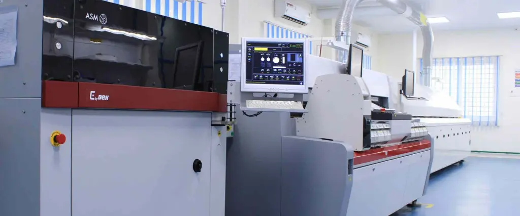
The electronics industry comprises the design, development, manufacturing, and sales of electronic equipment, parts, and components. This industry produces electronic parts and components for various applications. Therefore, it plays a crucial role in the development of various sector of the global economy.

Europe is well-known as a large manufacturer of electronics. Countries like Germany, the UK, France, Sweden, Spain, and more have contributed to the development of the global electronics industry. Here, our major focus will be on electronics companies in Sweden. We will discuss their market value, specialization, and what these companies offer.

Overview of the Electronics Industry

Smart Electronics Manufacturing

The electronics industry comprises organizations that deal with the design, development, manufacturing, assembly, and distribution of electronic components and equipment. These organizations provide various products that share one similarity: they operate based on electronic technology. The electronics industry is a fast evolving and innovation one. It is also competitive.

This industry keeps experiencing growth and development in different segments. In the electronics industry, investing in the research and development of new products is very important. This is crucial in an industry where companies and organizations want to remain relevant amidst competition. Therefore, these companies compete to be the first to introduce the most recent and advanced technologies to the market.

Electronics is an aspect of technology that involves the application and control of electricity in liquids, in semiconductors, and in gases. There are a wide range of electronic products. These products comprise subassemblies, materials, components, equipment, and parts that integrate electronics principle to carry out their functions.

In general, the goal of the electronics industry is to provide electronic products or parts to meet the growing needs of electronic producers. A lot of money and effort have been invested in the research and development of electronics to manufacture products and parts. The development of new electronics can require a huge amount of money and a lot f effort. This development might take time to orchestrate.

The electronics industry has been existing for centuries. This industry keeps evolving as new technology and processes are being introduced. However, this industry has continued to stand strong in the phase of challenges and economic crisis.

Electronics Manufacturing in Sweden

FULL PCB MANUFACTURING Quote

The electronics manufacturing industry is one of the main industries in Sweden. This industry has been experiencing growth for the past few years. The market size of the electronics manufacturing industry is said to grow at a fast pace. All thanks to the integration of advanced and most recent technologies in this industry.

According to a research, the electronics sector in Sweden will experience a 2.83% growth from 2023 to 2027. This will result in a market volume of about 4.4 billion dollar in 2027. The electronics companies in Sweden have been contributing to the global electronics industry. There are a wide range of electronics companies in Sweden.

In 2023, the electronics market is expected to experience an annual growth of 0.75%. Innovation is the driving force of this market. Also, constant improvement on existing products and creation of new ideas contributed to the growth in this industry. The electronics industry can be included among the most innovative and competitive industries in Sweden.

Top Electronics Companies in Sweden

Niob AB

This emerging Swedish company specializes in the production of consumer electronics. In 2004, the company launched its first product which was an mp3-player called NB-110. The design of electronic products takes place in Sweden. However, the production facility is located in China. This electronics company in Sweden focuses on investing in its expansion across the world.

Niob AB puts quality and functionality when developing their products. To achieve this, this electronic company ensures all of its products adhere to industry standards. Through the integration of cost-efficient technologies and processes,  Niob can offer low prices on its product without the need to compromise the quality and functionality of their product.  

This company believes their customers must get good value for their money. Niob hopes to continue with the development, manufacturing and sale of consumer electronics and as well have good partnership within this area.  Niob AB produces consumer electronics like video equipment, TV sets, and music players. As an innovative and unique electronics company in Sweden, this company is dedicated to offering top-notch products from a consumerโ€™s perspective.

Rejoy

If you are in need of an online provider of technical peripherals like spare parts video game accessories, Rejoy is the right choice for you.  This leading online provider of techincal peripherals  provides video game accessories for gaming consoles on the market.  In 2004, this swedish based company was founded.

It is one of the top leading providers of video game accessories in Sweden.  Rejoy offers new innovative products. Rejoyโ€™s strong relationship with gamers made it ranked as one the largest supplier of video game accessories in Scandinavia 2008. One of the benefits of working with this company is its focus on delivering the best to their customers.

Rejoy makes decision by prioritizing the interest of their customer first. This company ensures all products meet the needs and requirements of their customers. The team at Rejoy will support you all through the whole process of making your order and purchasing their products.

Zoro Industries

Electronic Equipment Manufacturers

This is an electronics company located in Stockolm, Sweden. With over 12 years of professional experience in consumer electronics manufacturing, Zoro industries has been supplying quality consumer electronics.  Zoro supplies a wide range of consumer electronics which include mobile phones, washing machine, computers, and more.

Zoro Industries doesnโ€™t just offer affordable products. All of its products offer high-performance and quality. Also, they provide aftersale services to their customers. With Zoro industries, you can never get it wrong. This electronics company is presently ranked as one of the best in Sweden.

Venus Electronics SB

This Swedish electronic companyโ€™s specialization is in the consumer electronics. Venus Electronics SB is a producer of consumer electronic products like video games, mobile phones, TVs, and digital cameras among others.  Venus Electronics SB has more than 10 years experience in the production of consumer electronics.

This company is ranked among the best electronic companies in Sweden because of its dedication to providing high-quality electronic products. Also, Venus Electronics SB is compliant to some standards in the industry. This company has its headquarters located at Stockholm, Sweden. As a large distributor of consumer electronics, Venusโ€™ products are sourced from well known vendors across the world.

They offer worldwide shipping. Also, they ensure customers get their products delivered within a short period of time. As a popular consumer electronics company in Sweden, Venus Electronics SB offers top-notch consumer electronics that meet the specifications of various consumers.

Hyperlife Technologies Ltd

Hyperlife Technologies Ltd is a renowned electronics company in Sweden. This company has a wide range of electronic products. You will find the most recent televisions, game consoles, and home appliances from various brands. All their offered electronic gadgets are guaranteed, new, and original. Also, these products usually come with about 2 years warranty.

Customers can enjoy the benefit of their 90 Days sales return policy. This policy allows customers to return any product purchase before 90 days. Therefore, if a product is defective, customers can return such a product. Hyperlife Technologies Ltd is dedicated to offering top-notch customer service.

Also, this company believes in satisfying the needs and demands of every customer. Therefore, they ensure customers receive value for their money. At Hyperlife Technologies Ltd, customers are guaranteed an effective shopping. The product portfolio of this company includes game consoles, LCD TVs and LED TVs. Also, the main market of this company is in Europe, Asia, America, and Middle East.

Electrolux Group

This is a global leader in appliance manufacturing. Electrolux Group has shaped human lives by providing high-performance home appliances. As a renowned Swedish electronic company, Electrolux Group has more than 100 years experience in the production of electronic products that befits a good lifestyle. This company is always at the forefront of sustainability through their operations and solutions.

Electrolux Group is one of the largest manufacturers of appliances for kitchen in Sweden. This Swedish company designs and manufactures a wide range of consumer electronics like refrigerators. In order to achieve their goal, this companyโ€™s model focuses on giving consumers outstanding experiences.

The team at Electrolux Group aims to create much desirable solutions and lovely experiences that will continue to enrich the peopleโ€™s lives. This electronic company is dedicated to investing relevant innovations that create the best products.

EG Electronics

EG Electronics provide cost-effective solutions to problems arising in the electronics manufacturing industry. This Swedish electronics company remains relevant in the industry by offering solutions based on electronic systems and components. They have got customers across several industries.

EG Electronicsโ€™ products are widely integrated across industries like medical, telecommunication, automation, and military. One of the greatest benefits of hiring or working with this electronics company is their compliance to industry standards. EG Electronics is ISO 9001 & 14001 certified.

With over 90 years of professional experience in manufacturing of appliances and electrical electronics, this company has continued to deliver the best. As a reputable electronics company in Sweden, EG Electronics work with a team of professional developers and engineers who work towards creating innovative solutions in the electronics manufacturing industry.

Northvolt

Northvolt is an electronics company in Sweden well known for manufacturing batteries. This company specializes in lithium-ion technology designed for electric vehicles. Peter Carlson, a former executive a Tesla Motors founded Northvolt in 2015. Northvolt has plans to increase its production of batteries.

Its plan to build a factory in Skelleftea  is said to be the largest milestone in Sweden. Northvolt  aims to offer the safest lithium-ion battery in the world. This battery is said to have a low CO2 footprint. This company has invested hugely in building two factories for manufacturing lithium ion batteries.

Northvolt believes that awareness of climate change is driving the electric vehicle battery industry. Hence, this increases the demand for vehicles with zero-emission. Reducing the cost of sustainable battery cells will help to achieve this.

Important Factors Startups Should Consider when Manufacturing an Electronic Device

With the increasing population, more demands are being made by electronic consumers. Also, new and innovative electronic products are being developed. Electronic manufacturers may invest a lot in bringing a new product to the market. In most cases, these manufacturers will seek to create a revenue stream for their brand and as well offers something that meets the demands of your customers.

Below are important factors all startups should consider when manufacturing their electronic devices.

Create a Proof of concept

You need to design a proof-of-concept prototype with the aim of developing a functional prototype. For electronics development, this indicates the integration of electronic modules. You need to prove that your electronic product functions as expected.

Be creative with funding

Designing and manufacturing a new electronic is an expensive process that involves development and manufacturing. You will need to be creative enough when funding a startup.

Consider engineering expertise

You will have to outsource the development of your product to a professional engineer. It is advisable to take the development of your product on your own. However, you can find someone that has technical expertise and experience as your co-founder.

Consider experience

This is one of the most crucial factors you need to consider. You need to evaluate the experience of an electronics manufacturer to know if your requirements are being met. Check what this manufacturer has produced in the past and who they have partnered with. You can as well go for a manufacturer who specializes in your project. This will save you money and time in the long run.

Conclusion

In general, the goal of the electronics industry is to provide electronic products or parts to meet the growing needs of electronic producers. A lot of money and effort have been invested in the research and development of electronics to manufacture products and parts. Electronic companies in Sweden keep contributing to the development of the global electronics industry. These companies introduce new products and create innovative ideas to transform the industry as a whole.

The components and process of PCB motor design

PCB motor design

Miniature electric motors, called printed circuit board (PCB) motors, have their stator and rotor built right into the printed circuit board. This design offers several benefits compared to conventional motors, such as a smaller size, less weight, and higher durability. The PCB motor design process is described in depth here, including every stage from conceptualization through manufacture.

Step 1: Requirements Definition

Identifying the requirements is the initial stage in the design of a PCB motor. You must ascertain the operational parameters, such as the necessary torque, speed, and voltage, to do this. The designer must also consider any physical restrictions, such as the motor’s size requirements and any external influences that can affect the motor’s performance.

Step 2: Conceptual Design

The conceptual design process can start after the requirements are complete. This entails developing an initial design that complies with the specifications and practical limitations. The designer often uses CAD software to produce 2D and 3D models of the motor.

Step 3: Magnetic Design

Magnetic design is a crucial phase in designing a PCB motor. The stator and rotor must provide the necessary magnetic field. In addition, the designer must consider elements like the number of poles, the arrangement of the coils, and the magnetic material employed.

Step 4: Electrical Design

Motor PCB

The designer can proceed to the electrical design stage when the magnetic design is complete. The necessary electrical components, such as transistors and diodes, must be chosen to manage the motor’s operation. The designer must consider things like the required voltage and current and the type of control circuitry.

Step 5: Thermal Design

Because overheating can result in early failure, thermal design is a crucial component of PCB motor design. According to the designer, we must thermally optimize the motor’s components and offer sufficient heat dissipation. Adding heat sinks, fans, or other cooling systems may be necessary.

Step 6: Mechanical Design

The actual parts of the motor, such as the housing, shaft, and bearings, are designed during the mechanical design phase. Therefore, the designer must consider elements like the material utilized, the necessary tolerances, and production limitations.

Step 7: Prototyping and Testing

The designer must make a prototype and test it when complete to ensure it adheres to the design specifications. In addition, a test rig may be necessary to evaluate the motor’s performance under various loads and temperatures.

Step 8: Manufacturing

The designer can proceed to the production stage if the prototype complies with the design specifications. Many methods, such as surface-mount technology (SMT) and through-hole technology, can create PCB motors (THT). However, the motor’s size, complexity, and volume requirements determine the ideal manufacturing method.

Step 9: Quality Control

A crucial step in the production of PCB motors is quality control. First, the manufacturer must guarantee the motors’ design requirements and lack of flaws. This may require tests including visual examination, electrical testing, and performance testing.

Step 10: Assembly and Integration

The motors may be put together and integrated into the finished product after they have been produced and tested. Other design factors, such as software for motor control and mechanical fusion with other components, may be involved in this.

What is the best PCB motor design software?

FULL PCB MANUFACTURING Quote

The popularity of printed circuit board (PCB) motors is rising due to their compact design, lightweight, and great efficiency. Engineers and designers utilize specialized software to develop, simulate, and optimize their designs for PCB motors. The greatest PCB motor design software currently on the market will be discussed below, along with its features, capabilities, and constraints.

Altium Designer

Engineers and designers frequently utilize Altium Designer, a feature-rich PCB design program, for various tasks, including designing PCB motors. The program provides several capabilities, including schematic capture, PCB layout, and 3D visualization. Moreover, Altium Designer has a simple library of parts to incorporate into designs, including motors.

The ability to simulate is one of Altium Designer’s core features. As a result, the program comes with various simulation features, including temperature analysis, power integrity, and signal integrity. These technologies allow designers to model how their designs operate under various circumstances and optimize them accordingly.

The simplicity of usage with Altium Designer is another benefit. The program features a user-friendly interface and several tutorials and resources to assist novice users in getting started. Moreover, Altium Designer provides cloud-based teamwork capabilities that let many team members work on the same design at once.

ANSYS Maxwell

The specialist electromagnetic simulation program ANSYS Maxwell designed motors and other electromagnetic devices. The program has several capabilities, including heat analysis, circuit modeling, and 2D and 3D electromagnetic field simulation. Moreover, ANSYS Maxwell provides a simple library of materials and parts to incorporate into designs, such as coils and magnetic materials.

The precision of ANSYS Maxwell is one of its main benefits. The computer program simulates the operation of motors and other electromagnetic devices under various situations using finite element analysis (FEA). This enables designers to maximize the effectiveness and performance of their creations.

Customization is a benefit of ANSYS Maxwell as well. Designers can adapt the software to suit their requirements using various customization tools, such as user-defined functions and macros, provided by the program. In addition, ANSYS Maxwell supports integration with other ANSYS products, such as ANSYS Mechanical and ANSYS Fluent, for a more thorough study.

Infolytica MotorSolve

A specialist motor design program called Infolytica MotorSolve helps create and analyze motors. The program has several functions, such as tools for optimization, temperature analysis, and 2D and 3D electromagnetic field modeling. Moreover, Infolytica MotorSolve includes a sizable library of materials and parts that are simple to incorporate into designs, like coils and magnetic materials.

The simplicity of use of Infolytica MotorSolve is one of its main benefits. The program features a user-friendly interface and several tutorials and resources to assist novice users start. Infolytica MotorSolve also provides a selection of optimization tools so that designers may enhance their designs for optimal effectiveness and performance.

Another benefit is combining Infolytica MotorSolve with other Infolytica products, like MagNet and ElecNet, for a more thorough analysis. Moreover, Infolytica MotorSolve provides connectivity with MATLAB and Simulink, as well as other third-party applications.

MATLAB/Simulink

A popular software package for modeling, simulating, and analyzing dynamic systems, such as motors, is MATLAB/Simulink. The program provides several capabilities, such as signal processing, control system design, system modeling, simulation, and analysis. Moreover, MATLAB/Simulink provides a simple library of building blocks and models to incorporate into designs.

Components required for PCB motor design

PCB Motor
PCB Motor

Miniature electric motors built onto printed circuit boards are known as PCB motors. These motors are essential in many applications where size, weight, and efficiency are crucial. Therefore, a PCB motor needs several different parts. Below are the essential elements necessary for PCB motor design.

Stator

The motor’s stator, a fixed component, houses the wire coils that produce the magnetic field. The stator is often part of the printed circuit board in a PCB motor. One or more wire coils are twisted around a central core to form the stator. The particular motor design and application determine the number of coils and the windings’ layout.

Rotor

The permanent magnets or other magnetic components that interact with the magnetic field produced by the stator are in the rotating portion of the motor called the rotor. We often install the rotor on a shaft supported by bearings in a PCB motor. The particular motor design and application determine the magnets’ number and arrangement.

Bearings

The rotor shaft is supported by bearings, enabling smooth shaft rotation. The bearings of a PCB motor are generally tiny, precise bearings made for high-speed, low-friction operation. The particular motor design and application determine the bearing type that is employed.

Commutator

While the rotor rotates, a commutator changes the current’s direction flowing through the stator’s coils. A commutator is not necessary for a PCB motor since the direction of the current may be electrically regulated with an H-bridge circuit. Nonetheless, specific PCB motor designs could still include a commutator for convenience or other reasons.

H-Bridge Circuit

An electrical circuit known as an H-bridge help control the current flow through the stator’s coils. Four transistors are essential in an H-bridge circuit to regulate the current direction. These transistors sit in a certain way. An electronic control system, such as a microprocessor, usually operates the H-bridge circuit.

Driver Circuit

The Driver circuit drives the H-bridge circuit, an electronic circuit that also regulates the motor’s direction and speed. Typically, a microcontroller, other electronic control systems, driver ICs, and other parts make up the driver circuit. Usually included in the PCB, a microcontroller or other electronic control system manages the driver circuit.

Power Supply

The motor gets its power from the power supply. The electronic control system or an external power supply typically provides the power supply for a PCB motor. The power source must deliver the necessary voltage and current for the motor to function effectively.

Heat Sink

A part utilized to disperse the heat produced by the engine while it is running is the heat sink. The heat sink in a PCB motor might be a separate part or built into the PCB. To effectively dissipate heat while keeping a low profile, the heat sink often consists of a material with high thermal conductivity, such as copper or aluminum.

Conclusion

In conclusion, there are many processes in the PCB motor design process, which are difficult and iterative and span from requirement specification through manufacturing and integration. To construct a motor that satisfies the needs and physical limits, designers must consider various parameters, including magnetic design, thermal design, and mechanical design. Nevertheless, PCB motors can give tremendous benefits with appropriate consideration and planning.

Understanding Everything About IoT Based Smart Irrigation System

IoT Based Smart Irrigation System

The majority of farmers utilize huge tracts of land, making it quite challenging to get to all of their corners and keep track of them. Uneven water drops are a possibility occasionally. This causes crops to be of poor quality, which further causes financial losses. This Smart Irrigation System, which makes use of the most recent IoT technology comes beneficial in this situation and makes farming easier.

The potential for automating the entire irrigation system is enormous with this smart irrigation systems. Here, we’re utilizing the ESP8266 NodeMCU Modules and a DHT11 Sensor to develop an Internet of Things-based irrigation system. In addition to automatically watering the plants based on the soil’s moisture content, the system will also send data to the ThingSpeak server to help in tracking the condition of the land.

This System will include the water pump that will be utilized to sprinkle the water over the ground depending on the moisture, humidity, and temperature of that surrounding area.

Automated Plant Irrigation Systems that delivers alerts via mobile but fails to do so on the IoT cloud was built previously. In addition, a circuit for a soil moisture monitor and a rain alert can be useful in the construction of a smart irrigation system.

What Is IoT Based Smart Irrigation System?

IoT Based Irrigation System

Using science and technology to conserve water while irrigating is the goal of a smart irrigation system. Moreover, smart irrigation uses soil sensors, weather sensors, and smart irrigation controllers. According to studies, smart irrigation technologies can drastically reduce water waste to about 40%.

Based on the soil moisture levels, the irrigation system determines when to add water to plants and how much water is required.

As the controller controls the water valves, the sensors built into the IoT based irrigation system check the current ground weather and humidity. Automatic irrigation is another name for smart irrigation systems. This mechanism determines when and the amount of water the plant needs. As a result, it is perfect for water saving management on lawns, farms, and other surfaces.

Moreover, IoT based smart irrigation systems use LORA, mobile Internet, remote sensing, and the IoT technologies. Based on soil and weather types, the irrigation system provides the appropriate quantity of water to plants to help in saving irrigation water.

This smart irrigation system primarily uses many technologies, including computer, sensor, as well as automatic control technologies. Moreover, it integrates spray irrigation as well as drip watering for gardens.

Intelligent irrigation systems irrigate plants automatically. High levels of precision are provided by this system.

Key components of smart irrigation

FULL PCB MANUFACTURING Quote

The availability of the smart irrigation controllers makes it easiest to define smart irrigation. These devices monitor the soil moisture or local weather conditions and alter their irrigation schedules in accordance with those measurements and other types of user-inputted requirements.

The changeable sprinkling or watering schedules of such systems are hence their key characteristic. Smart irrigation can be described as a technique that enables precise management of large-scale water needs and requirements of the large farm, therefore saving water and money.

Most significantly, you can be sure your plants were constantly at the proper level of moisture due to the system’s improved accuracy, which will improve their growth cycle.

Also, you may connect the smart irrigation systems using your tablet or smartphone for an added degree of control, as is the case with most smart systems currently on the marketplace. This enables you to make quick changes to the settings using a straightforward app, in addition to receive notifications or continuously updated information on your garden or lawn right on your preferred device.

This spectrum of control gives you the ability to manage the precise watering patterns and requirements of several sections in the single garden, providing smart irrigation systems with a game-changing control for the irrigation world.

The Distinction Between the Soil Moisture and Weather-Based Sensors

Weather-based as well as on-site sensors for soil moisture are the two main types of the smart irrigation controller. The best option relies on the location as well as the surrounding surroundings.

Smart irrigation controls based on the weather

Evapotranspiration controllers, often known as the weather-based controller, modify irrigation schedules based on local meteorological information. Evapotranspiration deals with the result of both soil surface evaporation and plant material transpiration. These controllers acquire local meteorological data and modify irrigation runtime so as to ensure the right quantity of water is applied to the area.

Temperature, wind, sun radiation, as well as humidity are the four weather variables that are used in data for ET weather.  It’s a highly precise method for figuring out how much water a landscape needs.

The weather based ET controllers come in three very basic configurations:

Signal-based controller generate the ET values for the grass surface just at site using meteorological data gotten from the publicly accessible source. This controller receives ET data after it has been wirelessly transmitted to it.

The pre-programmed water consumption curve, determined by past water utilization in various regions, is used by historic ET controller. Solar and temperature radiation can be accounted for in the curve. On-site controllers for weather measurement controllers employ weather information gathered on-site to determine how much water and ET should be measured continuously.

Smart irrigation controls use soil moisture sensors.

Smart irrigation controllers with soil moisture sensors monitor the content and soil moisture using one of many well-established methods. The sensors precisely gauge the level of moisture in root zones of trees, turfs, or shrubs whenever they are buried there.

There are 2 distinct sensor-based techniques for measuring soil moisture:

Suspended systems for cycle irrigation can be programmed using watering schedules, the start times, as well as durations just like conventional timer controllers. This system will halt the following planned watering whenever the soil has enough moisture, which is the difference.

Water upon demand irrigation does not involve scheduling the length of the irrigation.  It contains user-configurable upper and lower thresholds, and when the moisture level of soil falls short of preset levels, irrigation gets started.

Technology for Smart Irrigation: New Controllers

The use of the smart irrigation technology spans a wide range, including advantages for consumers. It’s crucial to select the best technology for the job if you want to save water.

Several sections of Oklahoma have watering limitations, thus this irrigation timer can be changed to reflect the permitted watering days. The climate-based controller as well as soil moisture-based controllers is the two primary divisions of irrigation controllers.

Controllers Depending on the Climate

Climate-based controllers, commonly known as Evapotranspiration controllers, modify irrigation schedules according to local weather. Evapotranspiration has to do with the result of both soil surface evaporation and plant substance transpiration. Such climate-based controllers collect information about local weather and modify the irrigation run-time so that the landscape always receives the right amount of water.

Controllers for Soil Moisture Sensors

Controllers for soil moisture sensor are a part of the second category of the smart irrigation controller. These controllers for Soil moisture sensors use the soil moisture sensors installed underground in the lawns’ root zone to assess water need rather than relying on weather information. The volumetric water contents of the soil is estimated by soil moisture sensors. The percentage of the total soil volume that is taken up by the water is known as volumetric water contents. After volumetric water contents reaches the user-defined thresholds, the controllers could be set to open those valves and begin irrigation.

Added-On Sensors for Smart Irrigation Technology

Soil Moisture Sensor

The preexisting irrigation system controllers can be coupled with the soil moisture sensor. Prior to a planned irrigation event, the sensor gauges the content of soil moisture inside its root zone and skips the cycle when the moisture level is higher than a predetermined level.

There are various soil moisture sensor types available, and before buying one, the user should make sure this sensor is compatible with their system. Many soil moisture sensors have soil freeze sensors that, if temperatures drop under 32 F, will stop this same irrigation cycle. Both wired and wireless methods are available for soil moisture sensors. The soil moisture sensors typically costs between $99 and $165.

Freeze and Rain Sensors

Freeze and rain sensors stop the cycle of irrigation during a freeze or rain event whenever watering is not essential, despite the fact that these sensors are not regarded as smart technology. Money, w ater, as well as runoff are all wasted when you water inside the rain. There are three distinct types of rain sensors, and each one has a particular function.

The first kind a rain sensor, which is still used today, uses a little basin or cup for collecting water; when the required amount has been gathered, the cup’s weight stops this irrigation cycle.

This second kind of rain sensors makes use of the dish containing two electrodes which are spaced apart from the cup’s base at a particular distance. The third kind of rain sensor is easy to maintain and dependable because it lacks the rain catch cup.

Conclusion

The IoT based smart irrigation system automatically adjust watering schedules as well as run times to suit particular landscape requirements. These controls greatly increase the effectiveness of outdoor use of water.

Hot Tips for Excellent Prototype Board Soldering

PCB prototype assembly suppliers

Are you an engineer who wants to learn how to solder prototype boards in-depth? If so, you’ve arrived at the ideal location. Although soldering isn’t easy, you’ll be an expert with the appropriate advice in no time. This article covers the various solder types available for prototype board soldering, their benefits, and the two main methods for making solder joints and electrical connections between components.

What is Prototype Board Soldering?

Prototype board soldering is a procedure of connecting circuit components to a prototype board. Before committing to a complete production run, the engineer must test the design on a prototype board, normally a printed circuit board (PCB). It is versatile and simple to alter. This capability is ideal for prototype designs that might need modifications during the development phase.

Types of Solder

When soldering a prototype board, using the right type of solder is important. There are threeย types of solder commonly used for prototype boards, namely:

1.ย Lead-Free Solder

Lead-free solder aids in forming electrical connections between parts and comprises metals other than lead. Since lead is poisonous and needs to stay out of the environment, lead-free solder is becoming increasingly common in the electronics industry. Tin-copper and tin-silver-copper (Sn-Ag-Cu or SAC) are the two primary forms of lead-free solder (Sn-Cu). The average melting points of tin-copper and tin-silver solder are roughly 183ยฐC (361ยฐF) and 217ยฐC (423ยฐF), respectively. Moreover, it has a higher viscosity and needs a hotter soldering iron to melt it. On the other hand, lead-free solder is unsuitable for all soldering applications since it is weaker and more brittle than lead-based solder.

Lead-free solder consists of metals that are stable and non-toxic, making it safer for the environment than lead-based solder. Lead-free solder is often helpful in applications requiring high reliability, such as aerospace, military, and medical electronics. It is also widely applicable in consumer electronics, automotive electronics, and printed circuit boards.

Advantages

The following are some of the main advantages of Lead-free solder:

  • Environmental friendliness: Lead-free solder is a better choice than lead-based solder in terms of environmental friendliness. Lead is a hazardous chemical that can harm human health and the environment. The Lead-free solder eliminates the possibility of lead contamination, and PCB assembly has a smaller environmental impact.
  • Greater Reliability: This solder is more reliable than lead-based solder in terms of durability. It is more suitable for usage in tough conditions since it can sustain higher temperatures and is more resistant to thermal stress. It is, therefore, a dependable choice for long-term use.
  • Better Electrical Conductivity: Lead-free solder is more electrically conductive than lead-based solder. It lowers the possibility of electrical resistance and can enhance the device’s overall performance.
  • Improved Solder Joint Strength: Lead-free solder offers a stronger connection than lead-based solder, which makes it less likely to break or fail over time. As a result, the gadget is more durable overall.
  • Improved Surface Finish: Lead-free solder produces a better surface finish on the PCB, perfect for high-frequency applications. The device’s performance may improve due to the lower signal loss or interference likelihood of the smoother finish.

2.ย Flux-Based Solder

FULL PCB MANUFACTURING Quote

ย Flux is a chemical substance that aids in lowering the solder’s surface tension and preventing oxidation. While soldering, flux helps ensure that the solder, the component, and the board make a solid bond.

There are several types of flux, including liquid, no-clean, and rosin. The most popular flux used in soldering is rosin flux, which normally consists of rosin, ethanol, and water. Engineers use rosin flux when soldering components to prototype boards to guarantee that the solder creates a strong bond with the component and board.

Prototype board soldering also uses liquid flux, commonly comprised of water, ethanol, and boric acid. When soldering components on prototype boards, liquid flux helps lower the solder’s surface tension and stop oxidation. In addition, no-clean flux is another type of boric acid and water. It is not necessary to clear off no-clean flux after soldering because it aids in lowering the surface tension of the solder and preventing oxidation. No-clean flux is equally helpful in soldering components to prototype boards as the other two types.

Advantages of Flux-Based Solder

Employing flux-based solder comes with the following merits:

  • Improved soldering: Flux-based solder aids in cleaning and preparing surfaces for soldering, which results in better soldering. This feature lowers the possibility of voids or weak solder junctions and increases the solder’s stickiness. Moreover, flux-based solder aids in avoiding oxidation, which can lessen the likelihood of failure over time.
  • Reduced Heat Damage: Flux solder aids in equal heat distribution, lowering the possibility of heat-related component damage. This solder paste is crucial when working with fragile or sensitive components easily destroyable by high temperatures.
  • Decreased Soldering Time: Flux-based solder helps speed up attaching components to PCBs. Flux aids in surface cleaning and preparation, minimizing the need for extra cleaning or preparation stages.
  • Improved joint strength: Flux-based solder produces a stronger bind than unsoldered joints, enhancing the strength of the solder joint. This aspect increases the device’s general longevity and lowers the possibility of failure.
  • Decreased Solder Bridge Risk: Solder bridges, which can result in short circuits and other issues, can be easy to avoid with flux-based solder. This possibility lowers the probability of the item’s damage and enhances overall performance.

3.ย Lead-Based Solder

The lead-based solder consists of a large lead content. Electronics manufacturers have long used lead-based solder, but recent years have seen a decline in its use due to safety and environmental concerns. Despite its drawbacks, lead-based solder has benefits, such as soldering prototype circuit boards.

Lead and tin are the primary ingredients in lead-based solder, though other metals, such as copper, can also be part of it. Manufacturers may vary in their specific formulations for lead-based solder. Still, it normally contains either a lead-silver or a lead-tin alloy (often called “lead-tin” solder).ย Lead-tin solder typically has a melting point of around 183ยฐC (361ยฐF), while lead-silver solder typically has a melting point of about 230ยฐC (446ยฐF).

Benefits of Lead-Based Solder

The Lead-based solder may not be environmental-friendly. However, the following are some of its advantages:

Low Cost: Lead-based solder is an appealing alternative for applications that are on a tight budget because it is very inexpensive.

High Melting Point: Lead-based solder can be more suitable for high-temperature applications since it melts at a greater temperature than lead-free solder.

Stronger joints: Lead-based solder produces a strong link between components, increasing the device’s overall endurance. This feature leads to improved solder joint strength.

Excellent Electrical Conductivity: Lead-based solder provides superior electrical conductivity, which can enhance the device’s functionality. In comparison to other forms of solder, it is also less prone to result in electrical resistance.

Soldering Techniques

Soldering is a skill that requires practice and patience. Several techniques can helpย ensure that yourย components areย in their correct position.ย The following are two of these processes:

1.ย Hand soldering

The hand soldering process involves using a soldering iron, flux, and solder to link two or more components on a prototype board. Hand soldering is a typical technique to create electrical connections and solder joints between printed circuit boards, components, or cables. For reliable and high-quality solder joints, the hand soldering procedure needs a high level of ability and experience. Although it is ineffective for soldering several components at once, it offers great control and flexibility over the soldering process, making it perfect for small-scale production and prototyping.

The soldering Process

The process involves the following steps:

  1. Preparation: The Board and components must be ready before beginning the hand soldering process. Cleaning the PCB and the elements is necessary to eliminate any dirt or debris that can get in the way of the soldering operation. Before beginning, the operator should inspect the Board and the components for any damage or faults.
  2. Flux application: The operator adds flux to the PCB’s regions where the components will go. Flux is a chemical substance that aids in cleaning the PCB and component surfaces and enhances the solder’s wetting to form a solid bond.
  3. Component placement: The operator then adheres the components to the PCB, ensuring they are in their correct positions and with the proper orientation. The tweezers assist the operator in holding the elements in place to prevent them from moving while soldering.
  4. Soldering: This step involves heating the joint between the component and the board using the soldering iron. The solder flows around the connection and forms a solid link between the element and the Board when the solder melts due to the heat. The user must, therefore, be cautious not to apply too much heat since this could harm the PCB or the components.
  5. Board Inspection: After soldering, the operator should check each connection to ensure it is correct and free of flaws like solder bridges or cold joints. Before moving on to the following component, he should fix any of these errors.
  6. Cleaning: The operator should clean the PCB after soldering all the components to eliminate any flux residue or other debris that could affect the performance of the final product.

2.ย Reflow Soldering

This technique involves using a soldering iron, solder, and flux in a controlled environment to attach two or more components to a prototype board. The engineer initially heats the components to a temperature just above the solder melting point in this procedure. Often, a soldering iron or hot air rework station helps this. Next, he covers the prototype board with solder after assembling the components. Due to its effectiveness and dependability, reflow soldering is a widely used soldering technique in the electronics manufacturing industry. It makes producing circuit boards in large quantities with uniform and excellent solder connections possible.

The soldering Process

The reflow soldering process typically involves the following steps:

  1. Stencil printing: A stencil helps apply solder paste to the board. The stencil ensures that the paste only sits where the components will go.
  2. Component placement: After that, please put the components where they should be on the board.
  3. Preheating: Heat the board until you have activated the solder paste’s flux. The flux aids in cleaning the board’s and components’ surfaces of any oxidation or contaminants.
  4. Reflow: After raising the board’s temperature, the solder melts and flows, securing the components to the board.
  5. Cooling: To finish the soldering process and harden the solder, cool the board.

Conclusion

Soldering prototype boards is a crucial stage in the production of electronics. Lead-free solder, flux-based solder, and lead-based solder are the three types of solder most frequently used for prototype circuit boards. Each solder has benefits and drawbacks of its own. Therefore, selecting the appropriate solder for the task is critical. Moreover, components can be easily attached to a prototype board using one of the two primary soldering methods: hand soldering or reflow soldering. Engineers may confidently solder their prototype boards and start their projects with this knowledge. Thus, don’t think twice and start working with your soldering iron. After all, the easiest way to learn to solder is to get in and start getting your hands dirty.

What is a PCB Transistor and How Can You Test it?

transistors

Before you can comprehend how a PCB transistor functions, you must first understand what a transistor is and what to check for when choosing one. Before you purchase a PCB transistor, you must learn how you should test one.

What is a PCB Transistor?

Transistors are electronic devices that regulate the flow of electrons and hence regulate electricity. It implies they are in charge of initiating and terminating the electric current flow. Its main function is switching as well as enhancing the quantity of electronic impulses passing via circuit boards.

PCB Transistor Types

PNP and NPN are the two distinct kinds of transistors, and each has a different circuit symbol. Each of both transistors, which are built of semiconductor materials, has a unique set of layers. NPN silicon transistors, which are the simplest to produce, are the most widely used transistors.

Any novice must always begin by understanding NPN since they’re the simplest to comprehend. If you comprehend the NPN, it’ll be simple to help you study the full transistor and its various varieties.

How to Read PCB Transistors

transistor Component

NPN and PNP are the two most prevalent varieties of transistors, yet all of them can be made in many ways and are unique. Learning about transistors and understanding how to interpret a PCB transistor are the initial steps. Once you have mastered reading, then the next step for you is learning ways of testing them.

Our article would explain and teach you through the process involved in the reading a PCB transistor.

It is crucial to test the transistors so you can determine whether they will be helpful or not. Start by locating the marking beneath or close to the transistor.

  • Search for a line, an arrow, or a triangle with sides as well as a line beneath that appears to link them.
  • Unless the PCB transistor lacks that line, use that line which comes out from the left like the base. The metal enclosure acts as a foundation in the event that such a line is absent.
  • The transistor should be positioned so that the line that comes out faces the left hand side.
  • Be sure to locate and highlight the triangle since this NPN collector would be pointed upward and your PNP collector would be pointing below.

Testing the PCB Transistor

FULL PCB MANUFACTURING Quote

In circuits, transistors play a crucial role, thus it’s crucial to make sure they’re functional. When they are flawed, the circuit fails as a result. Because of this, it is crucial that you test them in order to make sure they are operating as intended. Be sure you understand what is expected of you before you start the procedure. A step-by-step tutorial for testing a PCB transistor is provided here.

Step 1

Before testing your transistor, make sure that there’s no electricity flowing through the circuit by ensuring it is switched off.

The battery should then be removed after unplugging its AVC power connection. Make sure that there’s no power present on the circuit board before simultaneously touching a capacitor’s two terminals with any metal. To prevent turning off stored power, use the screwdriver with insulation at the handle end.

Step 2

Watch out for the transistor that you will be testing for its collector, base, as well as emitter leads. These leads on some transistors are labeled for simple identification. C B, E, and B will be imprinted on them. By being certain of the orientation of leads, you should request a catalog from your electronics supplier. You should have confidence because the placements of the points vary depending on the transistor.

Step 3

If your digital multimeter has the diode setting, use it in this step; if not, use ohms setting. If the transistor is operating in the analog environment, set it using a low ohm scale.

Step 4

Touch a lead from of the meter into a base lead whilst you place its other on your collector lead to check the reading of the collector in both base-collector directions. Review the reading then share your advice. The transistor would display a reading for one direction as well as infinity for the other if it is functioning properly.

Step 5

While touching a lead towards the base while the other connects to an emitter, you must check the reading of the emitter on its base in the two directions.

Reverse these leads to read the meter in an opposite direction after checking it. Similar to step four, anticipate one reading should display 600 while the other will show an unlimited number.

Step 6


PCB Transistor
PCB Transistor

Remove its base lead if the reading isn’t really near to 600 because other components might be affecting the reading. Disconnect the data from the PCB by melting its solder attaching its base lead onto it. Using the meter, check both routes from of the base towards the collector-base towards the emitter. When you’re done taking the reading for the meter, melt your solder, push this lead into the hole of the board, and then reinstall it.

Step 7

Here comes the last step. Following testing, you ought to be able to tell if the collector or base-emitter readings indicate 0 in the two directions or if both indicate endless tasks. Zeros indicate a brief period of time. Moreover, infinities are signs of the open transistor diode.

However you are welcome to look here if you’d like to know more regarding how to thoroughly inspect a circuit board.

Conclusion

Prior to making a purchase of a PCB transistor, you must be aware of the transistor that you intend to utilize. In order to ensure that you’re getting the best open that suits you out of the many variations on the market, you must take care of a few things. The majority of providers will classify transistors based on their intended usage or the power rating.

In addition, if you don’t know much or are unfamiliar with pcb transistors, then it is crucial to speak with a professional to avoid making a mistake.

Things to you need to know about Unitech PCB โ€“ A Quality PCB Manufacturer

Shengyi S1000h PCB

If you’re unfamiliar with Unitech Corporation, you might wonder about its reputation. Established in 1994 by Chinese tech entrepreneurs, the company has diversified its business to include solar panels. In this article, we’ll delve into its history & current operations, as well as explore its offerings of rigid-flex printed circuit boards & double-sided printed circuit boards. By the end of this piece, you should be able to recognize a Unitech printed circuit board and understand how it can benefit you.

Solar cell business unit

Unitech Corporation will make more money by separating its solar cell enterprise into a new company. However, there was a report that Unitech’s founders took money from people who bought homes for other things. A giant electronics maker from Taiwan, called Inventec, is also a part owner of the new company. We don’t know how much money the new business will make yet, but there are some signs that it might be successful.

Chinese companies that make solar panels must reduce how much they produce, or they will keep losing money. Also, a new administration might focus on more reliable industries than solar. Lastly, the company might have to stop making solar panels because they don’t have enough money. However, this could be good for solar panel makers in Taiwan.

Multilayer PCBs

nanya-pcb-material

Multilayer PCBs by Unitech are gaining popularity in numerous industries due to their lightweight construction and impressive functionality. These boards are helpful in various high-tech applications, including X-ray equipment, optical fiber sensors, atomic accelerators, & weather analysis devices. Multilayer printed circuit boards offer several benefits to both manufacturers & end-users, including budget savings and improved functionality. 

Multi-layer printed circuit boards, with their increased number of layers, require more design time and attention during manufacturing due to their complexity. Any imperfection can render multi-layer printed circuit boards unusable. However, the benefits of using these boards are significant. They are more effective than single-layer printed circuit boards and can withstand a range of humidity, temperatures, & pressure. Additionally, flexible multi-layer printed circuit boards are helpful for assemblies that require flexible construction methods or applications that involve bending. 

With the increasing complexity and miniaturization of electronics, the internal elements must keep up with the trend. Double-sided printed circuit boards have proven insufficient in achieving a balance between size & functionality. However, multi-layer PCBs can overcome these challenges effectively. Unitech’s multi-layer printed circuit boards provide an ideal solution to meet this requirement, offering numerous advantages over traditional alternatives. Below are some benefits of utilizing multi-layer printed circuit boards. 

Multilayer printed circuit boards are strong and protected, making them great for putting lots of electronic parts close together. The coatings are connected well and help control how electricity moves through the board. This lets people do more things with the board and saves money because it’s easier to put many parts on it. 

Unitech’s multi-layer circuit boards are beneficial for cars. They can handle hot and wet conditions well and are solid and trustworthy. They also follow safety standards for the environment.ย 

Rigid-flex PCBs

FULL PCB MANUFACTURING Quote

Unitech PCB is growing because more people want to buy electronics for cars and everyday life. They are making more “rigid-flex” circuit boards to meet this demand, which they think will help them send out many circuit boards to people who make electronics. They are also planning to use these circuit boards for phone parts and are working with other important circuit board companies like Rayming PCB and Assembly. 

The new circuit board called a “rigid-flex printed circuit board,” has parts that are both hard and bendy. When it gets hot, it won’t get more extensive in some directions. This circuit board is better than other types because it doesn’t use things that get bigger or wet. They usually make these boards with stuff like sticky glue and a special kind of plastic that bends. However, these materials can make the board more extensive and cost more money. 

Rigid-flex circuit boards benefit space and car technology because they make things more robust and reliable. They also eliminate the need for breakable wires and connections made with melted metal. People can use them in testing machines, tools, and cars too. So if you need a circuit board that can handle being hit, shaken, or put in hot or cold places, a rigid-flex board is a good choice. 

Rigid-flex circuit boards cost more to create, but they save money when being made. This is because they can fit lots of parts on one board, so you don’t need to use lots of boards. This is cheaper. They can also be made special for different things and fit into different shapes. They are suitable for trying out new ideas because they are easy to test, even if they need to be small.ย 

Double-sided PCBs

double layer pcb circuit board

Unitech PCB Corp. is a company from Taiwan that makes circuit boards & solar panels. They make circuit boards that have circuits on both sides and also ones with lots of layers. They also make a particular solar panel called a “mono-crystalline silicon” panel. You can find their things in many places in Asia. If you want to know about their circuit boards, click the links below. 

Many circuit boards only have circuits on one side, which means you can only put parts on one side too. But using a “double-sided” panel, you can put pieces on both sides. This is good because it makes the board smaller and takes up less space. When the board is being made, they can also put more metal on it, which can help it handle heat better. This means the board can be even smaller and cheaper to make. 

Single-sided & double-sided circuit boards both have good things about them, but they aren’t identical. Double-sided boards are harder to make because you must put parts on both sides. This makes it cost more money to make. If you don’t have much money, you might want to use a single-sided board instead. This will be cheaper but may not be as flexible as needed for your job. 

A single-sided PCB has metal lines on one side and is more affordable than double-sided boards. They are often used in things like electronics for regular people and factories. You can also order a “flexible” version of the board. This board is made from a flexible material, so you can bend it without breaking it.

Future of Unitech PCB

Unitech PCB has become more successful since it started. Customers & shareholders wonder how it will keep growing in the future. Many things make a business successful, so there isn’t just one answer. Unitech PCB has plans and a direction that links each project together. The business’s future looks good – what about yours? 

Panasonic has announced that it will start making OLED television screens in 2020 at its factory in New Zealand’s Marlborough region. The manufacturing process will use both Japanese & Chinese techniques. 

Conclusion

Unitech PCB is a company from Taiwan that specializes in making PCBs. Their goal is to offer high-quality products that are valuable to their customers. Unitech has many client options, like rigid-flex printed circuit boards, flexible printed circuit boards, and printable boards. They also allow you to choose the best PCB that fits your product.