Top 15 Taiwan Electronic Component Suppliers

components manufacturers

Taiwan has a highly developed, highly diversified economy with a significant industrial sector. Numerous well-known Taiwanese businesses, from semiconductor production to telecommunications, are leaders in their fields on a global scale.

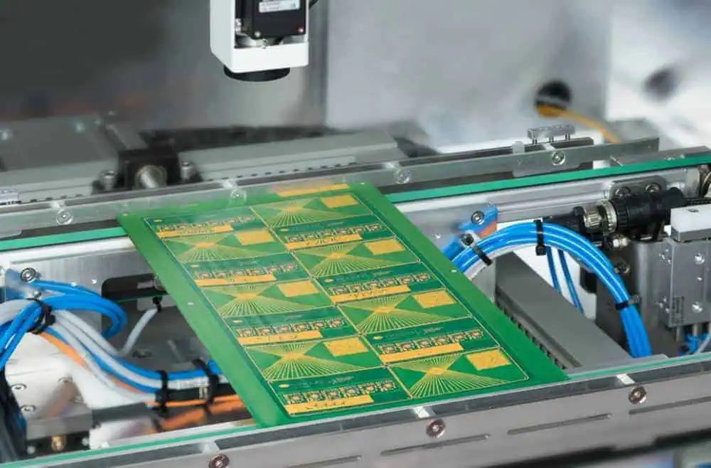
Due to its substantial ICT industrial base, strong semiconductor manufacturing clusters, and advanced manufacturing capabilities, Taiwan is a well-known ICT manufacturing hub. As a result, it has quickly developed many businesses that provide cutting-edge ICT-related goods and services. Main services are in telecommunications equipment, computers, fiber optic cable, electronic components, and information and communications technology. For US ICT providers, many Taiwanese businesses offer original design manufacturing services. Others have built robust supply chains that leverage US vendors as middlemen, enabling their enterprises to grow outside Taiwan into the US and other nations.

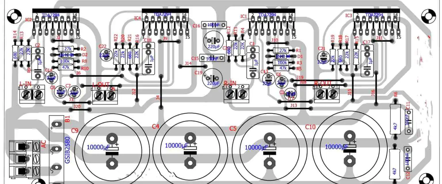
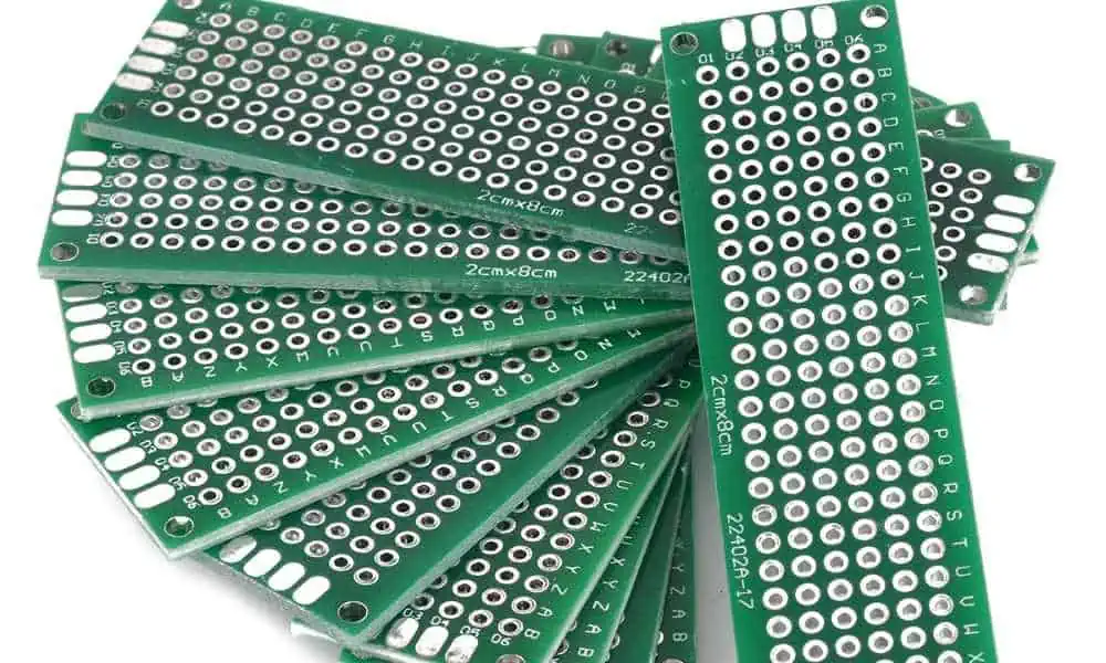
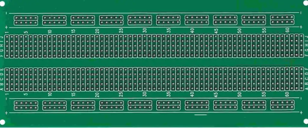
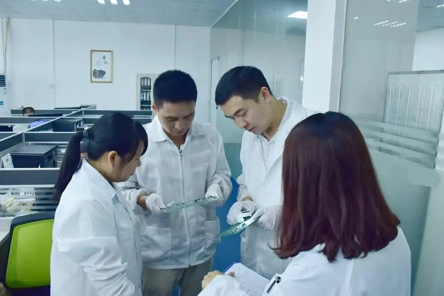
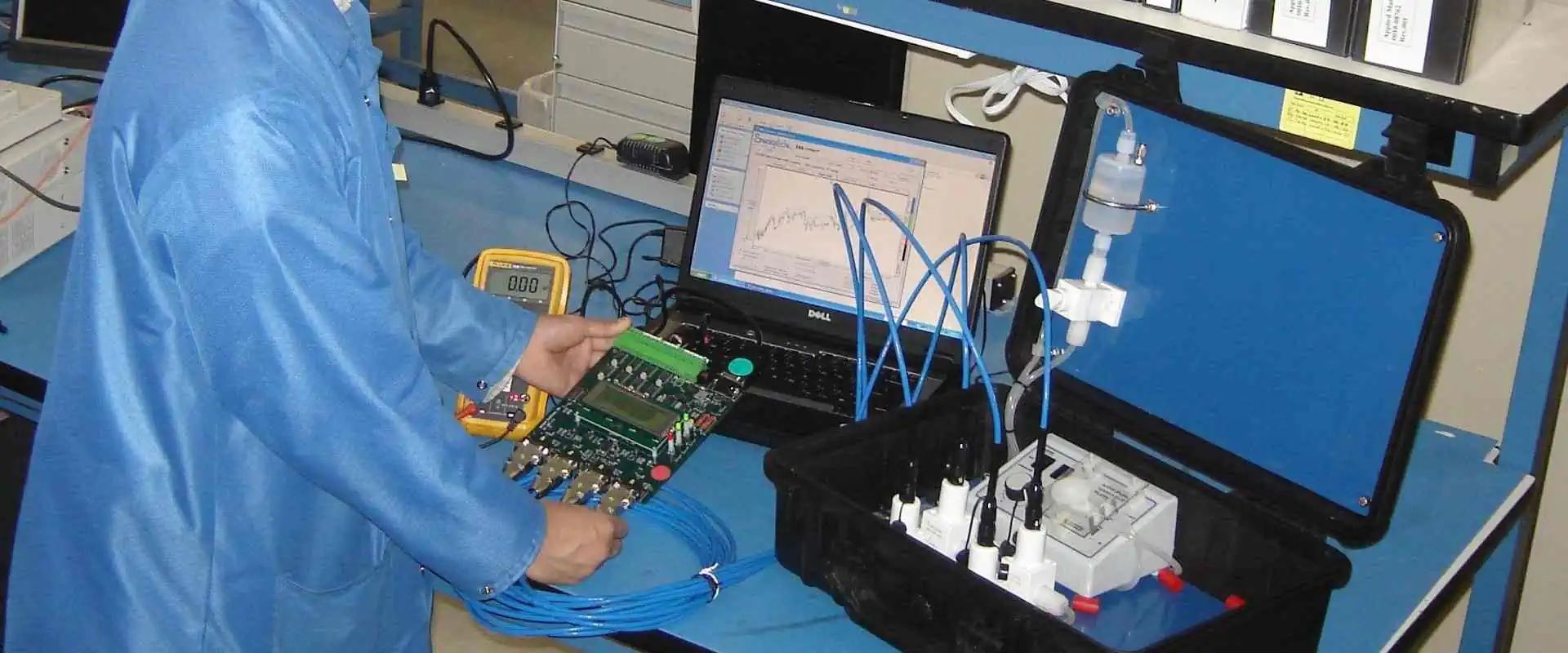
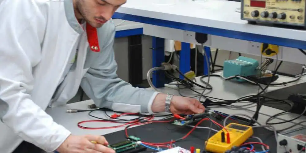
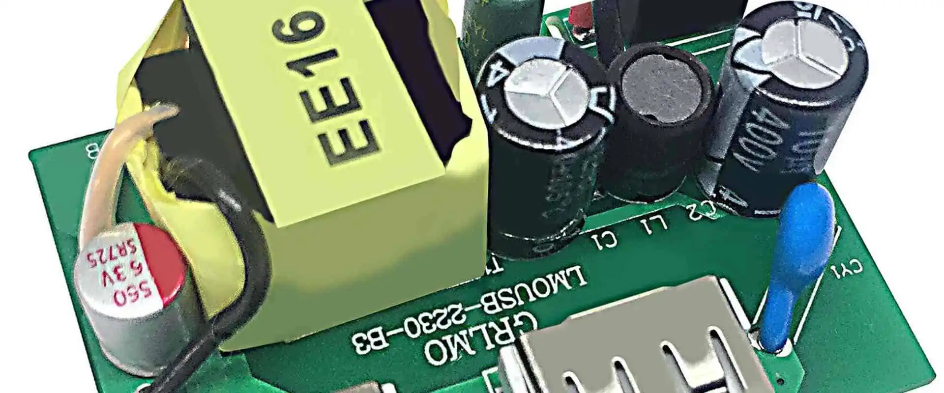
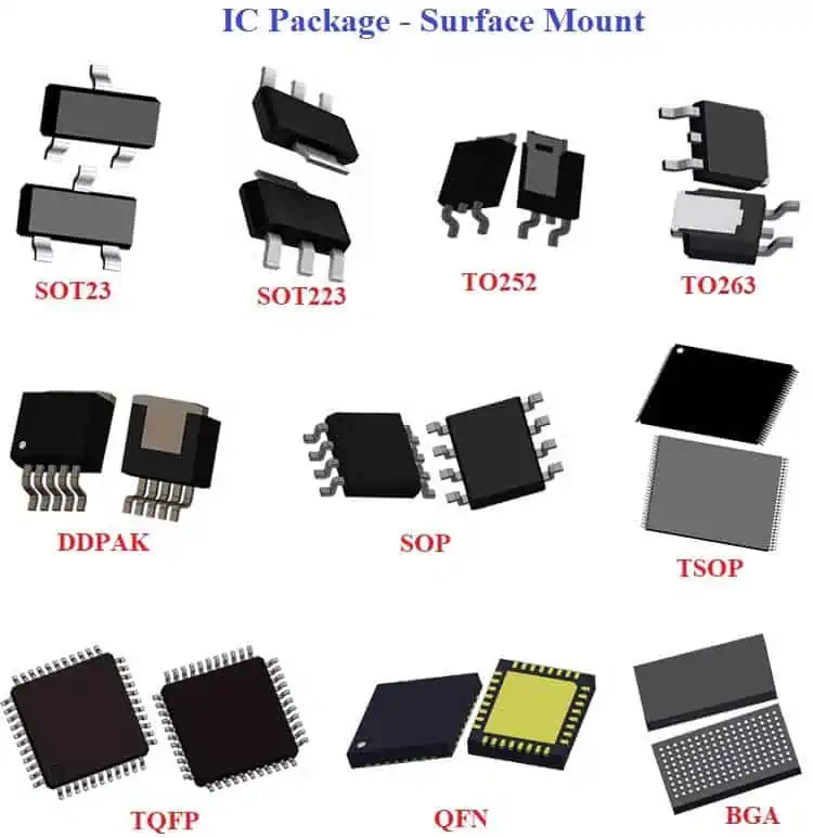
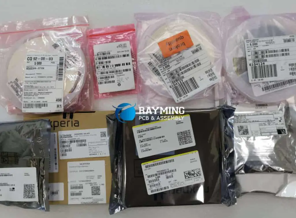
Taiwan electronic component suppliers

Leading global producers of electronics are Taiwanese businesses. Taiwan is still home to some of the greatest manufacturers in the electronics sector, even though most production has long since moved to Mainland China and other nations in the region. This directory includes Taiwanese electronics producers that provide a variety of goods and services.

The top 15 manufacturers of electronic components in Taiwan include:

MediaTek Inc.

Multimedia integrated circuit (IC) chipset research, development, manufacturing, and distribution are the main business activities of Taiwan-based MediaTek Inc. There are three divisions within the company. The first category, “mobile,” accounts for more than half of all sales, and MediaTek is the second-largest third-party provider of smartphone SoCs to companies like Xiaomi and Vivo. The second is “smart edge,” which includes the majority of non-smartphone gadgets and accounts for approximately 40% of sales. Finally, the third category is “power IC,” which covers items for managing power in data centers, networking devices, and more. The headquarters of Mediatek are in Hsinchu, Taiwan.

The primary items are mobile communication chipsets, tablet computer chips, Bluetooth chips, WLAN chips, GPS chips, optical storage chipsets, single-chip artificial intelligence Internet of Things devices, automotive electrical chipsets, and others. Additionally, the company offers services in associated design, testing, maintenance, and technological consulting. Mobile phones, digital TVs, personal computers, digital home appliances, wearable technology, and Internet of Things items are the primary markets for the company’s products. The company primarily distributes products in domestic and international markets.

TSMC (Taiwan Semiconductor Manufacturing Company)

FULL PCB MANUFACTURING Quote

Taiwan Semiconductor Manufacturing Corporation (TSMC) is a Taiwanese semiconductor business that develops and produces semiconductor chips for various applications, such as internet-of-things (IoT) devices, computers, cell phones, and other mobile and desktop devices. Right now, it is the biggest independent, specialized semiconductor foundry in the world.

The corporation has manufacturing facilities in Taiwan, China, and the United States. Advanced manufacturing techniques, such as 7nm, 5nm, and 3nm technologies, are used by TSMC to create semiconductors. Customers of the business include well-known tech firms like Apple, Qualcomm, and AMD.

The priority placed on research and development is one of TSMC’s main advantages (R&D). As a result, the company makes significant R&D investments, which has allowed it to keep its place at the cutting edge of semiconductor technology. Additionally, TSMC has embraced new manufacturing techniques, including extreme ultraviolet (EUV) lithography, which enables the creation of smaller and more intricate chips quickly.

In addition to having a solid reputation as a reliable business partner for its clients, TSMC is renowned for its stringent observance of intellectual property rights. In addition, the business is famous for its dedication to environmental sustainability, with a particular emphasis on lowering greenhouse gas emissions and minimizing their negative effects on nearby communities.

TSMC is a major force in the semiconductor industry, prioritizing R&D, cutting-edge manufacturing techniques, and environmental sustainability. Its chips power many different technologies and devices essential to modern life.

Delta Electronics, Inc.

An international corporation headquartered in Taiwan, Delta Electronics, Inc. focuses on producing power and thermal management products. Since its founding in 1971, the business has expanded to become a major player in the electronics sector, operating in more than 160 nations and employing more than 100,000 people globally.

Power supplies, industrial automation, networking products, and renewable energy solutions are just a few of the many goods and services that Delta Electronics, Inc. provides. Products from the company are essential in a wide range of industries, including renewable energy, data centers, medical equipment, transportation, and telecommunications.

Delta Electronics, Inc. has recently concentrated on creating environmentally friendly solutions, such as energy-efficient devices and renewable energy technology. As a result, the business has received various accolades and certifications for its environmental and social performance.

Walsin Technology Corporation

A Taiwanese business called Walsin Technology Corporation focuses on creating passive electronic components. Taiwan’s Taipei serves as the company’s headquarters. It was established there in 1992.

The passive electronic parts produced by Walsin Technology Corporation include ceramic capacitors, chip resistors, inductors, and varistors. Computers, cell phones, televisions, and cars are just a few electronic products and applications that utilize these components.

The business has factories in Taiwan, China, and Indonesia and sells its goods worldwide. Walsin Technology Corporation has achieved various certifications, including ISO 9001, ISO/TS 16949, and ISO 14001.

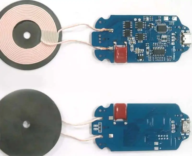
Walsin Technology Corporation researches and develops new technologies and products, such as wireless charging and energy harvesting, in addition to manufacturing passive electronic components. The company aims to establish itself as a market leader in providing cutting-edge electrical parts and solutions for the IoT (Internet of Things) and smart device industries.

Yageo Corporation

A multinational corporation with its main office in Taipei, Taiwan, called Yageo Corporation, produces passive electronic parts. Since its founding in 1977, the business has expanded to rank among the biggest producers of chip resistors, MLCC, and other electronic parts.

Many electronic gadgets, including cellphones, computers, televisions, and automotive systems, use Yageo products. In addition to having a worldwide network of sales and distribution channels, the corporation runs production sites in Asia, Europe, and the Americas.

Yageo is renowned for its dedication to quality and innovation and has won numerous awards and accolades for its operations and products. In addition, the business has undertaken various measures to lessen its impact on the environment and assist regional communities as part of its commitment to sustainability and social responsibility.

Lite-On Technology Corporation

circuit board electronic components

A Taiwanese business, Lite-On Technology Corporation, specializes in designing, developing, and producing various electronic goods and parts. Taiwan’s Taipei serves as the company’s headquarters. It was established there in 1975.

Products from Lite-On include solid-state drives (SSDs), optical disc drives, power supplies, LED lighting options, and other technical parts. In addition, lite-On produces finished goods under its brand and serves as an original equipment manufacturer (OEM) and an original design manufacturer (ODM) for other businesses.

China, Vietnam, the United States, and Europe are just a few nations where Lite-On has manufacturing plants and sales offices. Additionally, the business is dedicated to innovation and places a high priority on sustainability and CSR.

Nanya Technology Corporation

Leading manufacturers of dynamic random-access memory (DRAM) products include Nanya Technology Corporation. They specialize in designing and producing premium DRAM modules for various products, such as servers, mobile devices, and personal PCs.

The DRAM products made by Nanya Technology Company are renowned for their high quality, dependability, and performance.

The business makes significant R&D investments in DRAM technology’s bleeding edge, ensuring its products are continually current and provide cutting-edge performance.

In the DRAM market, Nanya Technology Company has a lengthy track record of achievement and enjoys widespread customer confidence.

The Nanya Technology Corporation is dedicated to environmental sustainability. Additionally, it has implemented several programs to lessen its influence on the environment.

Overall, Nanya Technology Corporation can be a wonderful option if you seek a reputable and trustworthy source of DRAM goods. However, before making any business decisions, you should always do your own research and due diligence.

AU Optronics Corp.

active and passive components

Liquid crystal displays (LCDs) and organic light-emitting diode (OLED) displays are among the flat panel displays the Taiwanese business AU Optronics Corp. manufactures and sells. Televisions, cellphones, tablets, and automobile displays are just a few areas the company supports.

Leading producers of flat panel displays, such as liquid crystal displays (LCDs) and organic light-emitting diode (OLED) displays, include AU Optronics Corp. The business enjoys a solid reputation in the display market for its technological know-how, which might provide a competitive edge.

Products available from the company include displays for computers, smartphones, tablets, televisions, and automobiles. With such a wide range of products, AU Optronics can appeal to a wide consumer base and create several revenue streams.

AU Optronics Corp. aims to deliver superior products that meet or surpass industry requirements. As a result, the business has won many accolades and certifications for its goods. They include ISO 9001, ISO/TS 16949, and 14001 environmental certifications.

With its dedication to quality, technological know-how, and customer service, AU Optronics Inc. has built trusting relationships with its clients. As a result, the business has retained long-term relationships with many of the world’s top electronics producers.

United Microelectronics Corporation (UMC)

With activities in Taiwan, China, Singapore, Japan, and the United States, UMC maintains its headquarters in Hsinchu, Taiwan. After Taiwan Semiconductor Manufacturing Company, UMC is Taiwan’s second-largest contract chip producer (TSMC).

The fabrication of wafers, the production of masks, and the production of integrated circuits (ICs) are only a few of the foundry services provided by UMC. Consumer electronics, communications, computing, and the automotive sectors are just a few businesses that use its products.

UMC is renowned for its cutting-edge technology and original approaches. It places a high priority on research and development and makes significant investments in cutting-edge manufacturing techniques. One of the world’s most cutting-edge semiconductor manufacturing facilities is UMC’s 12-inch fab in Tainan, Taiwan.

UMC is firmly committed to environmental preservation and sustainability. It has implemented several initiatives to reduce waste output, greenhouse gas emissions, and energy use in its operations. Also, the corporation has established challenging sustainability objectives, like becoming carbon neutral by 2050.

Winbond Electronics Corporation

Winbond Electronics Company designs, develops, produces, and sells large-scale integration integrated circuits (ICs) in Asia, the Americas, Europe, and internationally for various microelectronic applications. It functions through the Logic IC Product, Flash Memory Product, and DRAM IC Product segments.

The company also engages in electronic commerce, testing, OEM, computer software services, testing and consulting wholesale computer, supplement, and software business, and project sales. Additionally, it engages in research, development, design, sales, and after-sales service for semiconductors and 6-inch wafer products.

Advanced Semiconductor Engineering, Inc. (ASE)

The top company in the world offering semiconductor manufacturing services in assembly and testing is ASE, Inc. To meet the increasing momentum across a wide range of end sectors, including 5G, Automotive, High-Performance Computing, and others, ASE is introducing revolutionary advanced packaging and system-in-package solutions and a broad portfolio of well-established assembly and test technologies.

Chip manufacturers receive assistance from ASE in completing production. The business is among the top providers of semiconductor packaging services in the world. It designs and produces interconnect materials and offers front-end and final chip testing services through its subsidiary ASE Test. In addition, through Universal Scientific Industrial (USI), the business offers electronic manufacturing services. It also owns ISE Laboratories, a Silicon Valley-based company that offers engineering test services. A little more than 65% of ASE’s sales come from customers in the US. The firm has more than 240 clients worldwide, with Broadcom, Microsoft, NVIDIA, and STMicroelectronics among the biggest.

Largan Precision Co., Ltd.

Largan Precision Co Ltd creates, develops, produces, and sells plastic aspherical lenses and optical components (Largan). The company’s product offerings include webcams, cameras, cellphones/NB, automobiles, and scanner lenses. Printers, optical mouse lenses, wearable technology, in-display optical fingerprint recognition, and automobile lenses are just a few of the devices that Largan’s products use. Moreover, the company makes contact lenses, voice coil motors, and sleep monitoring. Taiwan and China both have largan manufacturing facilities. It sells its goods across the Americas, Europe, and Asia. Taichung, Taiwan, serves as the company’s headquarters.

Catcher Technology Co., Ltd.

The processing and production of integral castings made of aluminum and magnesium and parts and components for communications and consumer electronics goods are from Catcher Technologies Co Ltd (Catcher). Additionally, it offers several castings for laptops, desktops, servers, industrial computers, and other accessories, including power tools and automobile castings. Consumer electronics made by Catcher include camcorders, digital still cameras, and related accessories. The business also researches and develops plastic, fiber, stainless steel, zinc, magnesium, and aluminum materials. It runs businesses in China, Taiwan, the British Virgin Islands, Hong Kong, and the Philippines. The main office of Catcher is in Tainan, Taiwan.

Formosa Taffeta Co., Ltd.

The main activities of Formosa Taffeta Company Limited are the distribution of textile products and the weaving, dying, printing, and finishing processes. In addition, it supplies yarn, cotton, special textile, cotton, cable, nylon, fabric, and other related items. The company was founded in 1973 and had its headquarters in Taiwan’s Yunlin County.

The weaving, dyeing, and works industries are involved in producing a variety of plain woven textiles as well as mixed fabrics, staple fiber fabrics, long and short woven fabrics, and polyamine & polyester fabrics. Polyamine and polyester tire cords, functional yarns, pure cotton yarns, mixed yarns, special & unique protective yarns and textiles, composite fabrics, bulletproof fabrics, medical care fabrics, carbon fiber fabrics, and plastic bags are all provided by the cords and industrial materials businesses. The oil products industry runs gas stations where goods are sold, along with vehicle wash facilities. So, the Formosa technology firm assembles, tests, fabricates, and develops a variety of integrated circuits.

Kinpo Electronics, Inc.

They offer comprehensive manufacturing solutions for all clients. It includes well-known international companies, and does so with the finest benefits of vertical integration, clever production, and digitalized management. It pays close attention to every production stage. Via a thorough supply chain and a production system of internal suppliers, they want to assist clients in lowering costs and working toward an early product launch.

Kinpo Electronics may offer product design, cost, and production services for various consumer electronics. They can provide big multinational brands with suitable services in the design, production, and sales of consumer electronics thanks to our experience spanning more than 40 years. As a result, the consumers genuinely appreciate the service provided by our speedy product launches and low prices while still receiving high-quality products and competent delivery.

What are the Properties and Applications of the TDA7294 PCB?

TDA7294 PCB

The TDA7294 can be described as a unique amplifier as well as sound system circuit system. According to the company’s claims, it is unrivaled in terms of its potent performance. The business has been active in China. Also, it can be regarded as the most recent and modified of the various amplifier circuit variations. Regarding previous issues that happened with other types, this circuit amplifier remains trustworthy.

These circuits are still used today in a variety of electrical devices. It’s an important chip whose design progress is noteworthy. The chip handles smooth tones and provides faultless bipolar signal processing. Power MOS are supported by the circuit.

This chip comes in a variety of quality. Several of these offer strong resistance and overheating defense. Also, it provides less distortion as well as less noise.

Amplifiers work exceptionally well thanks to the combination of all these features. The chip can also be described as mono amplifier IC (integrated circuit), further defining this sort of circuit. This includes a Multiwatt15 individual bundle. Such tools are beneficial for unique audio-focused amplifiers. They are typical in both homes and workplaces.

These amplifiers seem to be the best at producing voltage and controlling various ohmic resistance ranges. Regulation is made simpler for users using this chip. These chips have a built-in feature that lets you switch between muting and unmuting the noise that electronics make.

What Does TDA7294 Offer?

TDA7294 PCB
TDA7294 PCB

The output power of the monolithic IC or integrated circuit TDA7294 is high (can reach 100W) and is designed for usage in audio amplifiers especially in the Hi-Fi field application i.e. Topclass TV, Home Stereo, and self-powered loudspeakers.

It can supply the most power into all of the 8W and 4W loads regardless of the presence of the regulation of poor supply and voltage rejection in high supply because of its wide range of voltage and high out capability of the current. The integrated muting feature plus turn-on delay makes remote operation simpler by preventing switching on and off the noises.

A growing market in the consumer electronics exists for monolithic audio amplifier with extremely high power that can equal the performance of the finest discrete devices while remaining reasonably priced.

The occurrence of the second breakdown phenomena makes it extremely challenging to realize the linear integrated circuits using traditional bipolar technology.

It restricts the power devices’ area for safe operation therefore, as a result, the maximum output power that may be achieved, particularly when very reactive loads are present.

In addition, because sophisticated protective circuits are required for complete SOA exploitation, layout and circuit complexity significantly increases. The usage of the powered MOS devices, that are resistant to a secondary breakdown, seems highly recommended to get over these significant limitations.

As a result, the stated device was created using the BCD 100 bipolar-MOS mixed high-voltage technology.

What are the Features of the TDA7294 PCB board?

keypad board
keypad board
  • The TDA7294 PCB has a higher working voltage range of 40 V
  • DMOS power phase, which is essential for a variety of activities
  • High output powers which supports as much as 100 Watts of music and does not require smd components
  • Muting as well as standby functions enabling user convenience while operating
  • No button to turn on and off any noise to ensure more feasibility
  • Does not have boucherot cells which makes it less expensive
  • Produces little noise and uses few components
  • Guards against overheating and dangerous sparks
  • Also, there is thermal shutdown where necessary, which is a particular feature of the circuit diagram.

The need for these amplifiers is increasing in the electronics industry. It is crucial to create inexpensive amplifier circuits because their use is growing every day. They should be taken into account when creating unique and irresistible prototypes or designs.

Modern technology that creates circuitry to be utilized this way supports the production. The breakdown process in this instance is a drawback. It limits the production’s safe operating region. As the electronics want a specific output in regard to their power supply, it becomes more inevitable. In this instance, the loads are entirely reactive. This same existence of the SOA causes circuit layout to change more, and also a rise in circuit intensity.

It is crucial to the high-quality operation of these circuits. Preventative actions can be taken to avert these delays and issues. Unique MOS electronics as well as their counterparts exist that can withstand and survive the breakdown issue. Certain technology, like the BCD 100, has appealing qualities. They are trustworthy for the voltage and usually seen as the bipolar mixed MOS devices.

Output Stage of the TDA7294 PCB Boards

Visual Components Assembly

A difficult aspect of design development is the creation of the design. A complex circuit system which is essential for amplifiers is also part of the procedure. The goal is to streamline this process’ output step. One thing is for sure, though: the constructed buffer must be able to regulate the dangerously high current voltages that are generated. This is accomplished by controlled distortion and careful attention to the frequency as well as its effects.

The importance of such quiescent current component cannot be understated. It must be regulated in order to maintain the integrity of all processes. With the aid of specialized feedback known as linearizing feedback, which is produced by such an amplifier, its quiescent current could be managed.

Some people believe that eliminating all bias will resolve this problem. This will not be enough to get rid of a crossover distortion, which can be very annoying. It is crucial to consider the dynamic aspect of the overall process whereas this DC is being sustained in its linearization. The goal of this phase is to eliminate the distortion to the greatest extent feasible.

High-efficiency

When it involves the implementation of the problems addressed by our electronics sector, there are many restrictions. These solutions deal with the issues of power and heat dissipation. They are beneficial for controlling the supply of power as well. These problems occur when AB-type amplifiers as well as their applications are used inefficiently.

The TDA7294 can be described as a unique amplifier that only functions within a specific voltage range. Thus, it can produce currents within a particular range, making it an effective voltage amplifier. Power dissipation and power supply size are obstacles to deploying high-power systems. These two conditions are brought on by the ineffectiveness of traditional AB class amplification techniques. This has a number of drawbacks, one of which being the uncontrolled power dissipation which results when the power range is exceeded.

Protections of the TDA7294 PCB Boards

While developing a power IC, special consideration must be given to circuits responsible for shielding the device against overload or short circuit circumstances. The DMOS transistors’ power is only defined by a maximal dissipation curve that depends on the length of an applied stimulus because the second breakdown phenomena is absent.

The protection method employed by this device blends traditional SOA protection circuits with a revolutionary local temperature technique for sensing that “dynamically” manages the maximal dissipation so as to fully utilize the potential of these power transistors.

Basic Facts Regarding the TDA7294 PCB

TDA7294 is an AB-type amplifier chip that is part of the monolithic group that uses the DMOS output mechanism. The chips excel at tolerating a variety of resistance within ohms ranges.

The chip is dependable for protecting the system from thermal issues and is supporting of various packages usually in watts. Such amplifier chips are mostly used in powerful speakers. They are used to give these loudspeakers the appropriate bass and volume.

It enables hassle-free and inexpensive replacement. Any device with a specialized heat sink as well as an astonishing several watts range can be linked to this amplifier chip.

The ability of these devices to function with maximum power and excellent efficiency seems to be another impressive characteristic. Because of the inclusion of analogues like the mute function as well as standby standard component option, the chip lowers noise loss caused by switching.

What are the Applications of the TDA7294 PCB?

Here are a few of the main uses for the amplifier chip:

  • Conventional subwoofers and audio systems
  • Standard bridge circuitry
  • Radio and Television
  • Loudspeakers

Conclusion

It ends here. This document offers all the relevant information regarding this amplifier chip. TDA7294 PCB is also available at your neighborhood electronics retailer. For the convenience of all the users, every application and how it functions is described in full. These chips offer essential uses in common household appliances which are utilized often in many houses. The need for these amplifiers is increasing in the electronics industry. It is crucial to create inexpensive amplifier circuits because their use is growing every day. They should be taken into account when creating unique and irresistible prototypes or designs. These circuits are still used today in a variety of electrical devices. It’s an important chip whose design progress is noteworthy.

What is a Universal PCB?

universal pcb

Any circuit board utilized during the design for prototyping ideas and validating system concepts is referred to as universal PCB. The creation of new machines and gadgets that are PCB-compatible depends on the universal PCB.

To prevent waste of money and time, they are extremely important in assisting manufacturers in perfecting the PCBs’ functionality before moving into mass production. The production of standalone electronic device components is a significant additional application for the prototype PCB.

In contrast to the phenolic paper that emits brown color linked with the brown PCBs, the majority are constructed of glass fiber. This is so that glass fiber can be used, which is more economical and more durable.

Holes of circuit boards are frequently tinned by some manufacturers to prevent oxidation and facilitate soldering. The majority of universal PCBs include soldering pads for connecting components, however some also have the spring terminals that are more suitable to hobbyist projects than intricate designs.

Description of the Universal PCB

Universal Circuit Board

Universal PCBs come in a variety of forms, dimensions, and styles, ranging from large circuit boards having sides measuring a few dozen centimeters in length to the rectangular PCBs which are nearly postage stamp-sized.

There are also boards available in the shapes of the euro cards featuring edge connectors as well as spherical PCBs, that are designed for computer card prototypes and LED illumination, respectively. They come in single-sided as well as double-sided versions and are made of paper laminates and glass-epoxy laminates with a range of thicknesses between 0.7 and 1.6 mm.

Despite the market’s diversity, the majority of universal PCBs adhere to an unwritten industry standard regarding dimensions. The boards often come in a set of between five and ten pieces, with each measuring roughly 5 ร— 7 cm, and are typically double-sided when you buy them from websites. Typically, its thickness is 1.6mm. The length of each grid equals roughly 2.5 mm, while the diameter of each hole is roughly 1 mm.

Even with all the advantages that circuit board prototype universal pcbs have, when it involves mass production of any tried-and-true PCB concept, the discussion always returns to circuit boards. The large-scale production might not necessarily result from the case.

The current project might be small and only involve singular units. Nonetheless, the majority of electronic projects which require a general-purpose Circuit board for the prototyping seem to be near the conclusion of mass production.

As a result, using universal PCBs is much more temporary and using circuit boards that are well known is much more permanent. Now let’s talk about circuit boards as well as how they highlight prototyping’s beauty.

Which Types of PCBs are There?

FULL PCB MANUFACTURING Quote

One sided PCB

There is only one layer of base material or substrate on the one-sided PCB. On one end of the substrate, a thin metal layer, usually copper because it’s a good electrical conductor, can be applied. When a protecting solder mask often is placed on top of a copper layer’s peak, the finishing silkscreen coat might well be applied to the top to identify the board’s components.

This PCB has many circuits as well as electronic components on just one side. This type of module actually works for the simple circuits, thus beginners commonly design and build such a board initially.

Two-sided Board PCBs

In comparison to single-sided boards, this type of Pcbs is much more prevalent. Elements are connected to the two sides of the board’s substrate, which has some conductive layers of metal on both sides. Circuitry solely on a single side of the PCB can connect to circuitry located on the opposite side thanks to holes in the PCB.

Multilayer PCBs

These PCBs have extra layers coupled with the bottom and top layers present in the double-sided construction, which makes PCB designs more complicated and dense. With access to several layers in such arrangements, multilayer PCBs allows designers to produce exceedingly thick and intricate designs.

Power planes that serve as extra layers in the design, provide the power circuit supply while also lowering the levels of the electromagnetic interference which are emitted through designs.

Universal PCB Printing

fr4 Epoxy Resin

Depending on what etching type is employed for PCB production, a circuit board’s materials and tools can differ dramatically. Yet regardless of whether etching can be carried out manually, with the aid of a machine, or using a chemical etching solution, there’s a standard tools set, which are useful, these include a printer and a PC.

Some supplies you’ll need include PCB boards that are photosensitive, transparent slides, cotton buds, Indian ink, paper towels, source of UV light, Drill bits, two glass or plastic bottles, two 1L bottles that are empty, rubber gloves, photosensitive circuit boards, fine sandpaper and perhaps kitchen scrubber, hydrochloric acid, acetone, thinner, and kitchen cleaner. Other items include copper boards, and hydrogen peroxide.

Depending on a number of variables, printing can use a variety of different procedures. Some methods include:

Acid Etching

The process employs a range of materials, such as the etchant, is quite slow, and therefore necessitates numerous safety measures. Depending on what materials you choose, the PCB’s quality you receive will vary, but broadly speaking, this is a decent solution for circuits having low to a medium degree of complexity.

Method of Routing

Specialized equipment which can mechanically eliminate extra copper out from board or install empty separators across wires is needed to use this procedure. One of these equipment can indeed be costly to buy, and renting it typically requires access to any nearby workshop. But, if you frequently need to duplicate your circuit and create high-quality PCBs, this approach is fantastic.

What are the Applications of the Universal PCBs?

Medical device

The healthcare sector uses PCBs more and more as technology advances and unveils new potential. A wide range of devices, such as those for therapy, monitoring, and diagnosis, make use of PCBs.

PCBs inside this industry frequently need to follow strict sanitary rules, especially during their implantation. Moreover, boards for a variety of applications, including ER monitoring, must be extremely small.

Consumer Electronics

PCBs are necessary for the operation of a wide variety of many other consumer goods. As more goods include electronics, Circuit boards become increasingly prevalent in our everyday lives. Small PCBs having a lot of connections are needed as manufacturers create smaller cellphones and laptops having improved capabilities.

To keep the price of consumer electronics low, PCBs must likewise be reasonably priced. Manufacturers also desire reliable boards because their ability to remain in business depends on the performance of their goods.

Industrial Equipment

The majority of the machinery in manufacturing as well as the distribution facilities, coupled with other industrial buildings, is powered by electronic components.

PCBs utilized in industrial sector typically need to be exceptionally powerful as well as long-lasting to withstand very harsh conditions present in industrial buildings.

PCBs must be protected from vibration, abrasion, extreme temperatures, as well as harsh chemicals when they are utilized in industry. Industrial PCBs might well be thicker compared to the other PCB types and made of materials which can endure high temperatures so as to meet this demand for durability. The industrial PCBA services may use through-hole technology to increase the strength of the boards.

Automobile Industry

Electronic components are being used in automobiles in increasing numbers. Originally restricted to headlight switches and windshield wipers, PCBs now offer a variety of cutting-edge technologies that improve safety and ease of use while driving.

Depending on its application, a PCB could need to tolerate extreme vibrations or temperatures. Additionally, it’s essential that they function reliably when they’re included in the car security feature. Manufacturers may use high-temperature laminate, copper or aluminum substrates, or thru-hole mounted components to address these problems. They also employ flexible stiff PCBs due to their resistance to vibration.

Ironing the Printed Universal PCB Layout    

 The schematic of the paper circuit and circuit board must be oriented. The schematic should be facing the circuit board’s copper portion. At this time, your iron ought to be on. Wait for the heating up of the iron after setting it to cotton setting.

The iron has to be heated up before being placed lightly on your paper top covering your circuit board. The iron must stay in position for about 30 to about 45 seconds. Carry the PCB to the closest water source after lifting the iron then carefully setting it aside. Avoid detaching the paper from the pcb board; it should be adhered to the board.

Hold your circuit board firmly down when the water begins to flow. After then, the paper would begin to gently and fully flake off. You could try soaking for a little bit longer when you find that some regions are particularly challenging to accomplish.

You should have the copper board having your PCB pads and signal traces etched out into a black toner if everything goes according to plan. Large water droplets could be easily removed by dripping them out or by gently wiping them off with a sponge or napkin.

Conclusion

Universal PCBs come in a variety of forms, dimensions, and styles. It also has countless uses and different applications.

The Properties and Uses of Fiberglass PCB

Shengyi WLM1 PCB

Printed circuit boards are made from a variety of materials. Fiberglass is widely used to create PCB laminates. This substance has been helpful for contemporary PCBs. Fiberglass-reinforced laminate composites are incredibly advantageous for the most common uses.

The use of fiberglass PCB has increased as advances in technology have occurred. There is new fiberglass provided with the strongest resin systems as well as improved properties. This material satisfies the performance as well as price requirements of our electronic industry.

Why the Fiberglass (FR4) Substrate is Important

In addition to being the standard rating, FR4 is also a name that can be spelled as FR-4. Epoxy-laminated sheet with fiberglass reinforcing used for the manufacturing of circuit boards are referred to by this nomenclature.

Yet, this word also designates a certain grade of epoxy laminate sheets. The grade is applicable to a wide variety of designs as well as sheet materials and is typically thought to signify the fundamental quality of a laminate sheet. The “FR” inside its name denotes that the material is flame resistant, and the “4” sets it apart from others in similar category.

The chemical commonly known as FR4 is constructed from composite components. The foundation layer of the material is made of fiberglass which has been weaved into a thin sheet that resembles fabric. The fiberglass gives FR4 the necessary structural stability.

The interior fiberglass layer is then encased and joined with a flame-resistant glue. The resin can be described as what imparts rigidity to a material along with other physical properties. Electrical engineers and designers like using FR4 sheets as the foundation for PCBs. The material’s accessibility, versatility, and broad range of beneficial physical properties might be blamed for its popularity.

FR4 sheets are electrical insulators with a high dielectric strength. Moreover, they have a strong strength to weight ratio, are moisture resistant, and are light in weight. When you add its temperature resistance to their ability to perform in most environmental conditions, FR4 material is a good choice.

What Advantages Does FR4 PCB Materials Offer?

FR4-PCB-Material

The term FR4 stands for flame retardant, and the number 4 designates a rating that distinguishes the material from others. FR4 is described as a woven, and thin fiberglass-reinforced epoxy laminated sheet used in the production of PCBs.

The substance’s FR4 composite fiberglass structure is what gives it rigidity as well as stability.

These benefits of FR4 make it a popular material with OEMs and PCB producers. Let’s look at them in the context of that.

Outstanding electrical properties

Electrical properties of a circuit board material are essential in the signal impedance as well as integrity calculations because they influence how rapidly any electrical signal moves through a specific material.

The high dielectric strength of FR4 is what gives it its electrical insulating properties. The thickness, kind of fiberglass weave, and resin employed all affect its FR4 Dk, which varies between 3.8 to 4.8 MHz.

Flammability retardant  

Flame retardants can be used in a wide range of production procedures and produce reliable results. Because of its superior electrical, mechanical, and thermal properties, FR4 is indeed a preferred material for majority of electronics applications.

Moisture Absorption

This can be described as one of the most important properties of FR4 materials. When immersed in water, the material absorbs moisture at about 0.10% rate. The FR4 was primarily moisture-resistant, however it is additionally temperature resistant and can withstand a wide range of temperatures.

Efficiency of Cost

FR4 is a well-known foundation material of circuit boards because of its inexpensive cost and stable chemical as well as physical properties. This benefits a lot of PCB manufacturers and designers that are concerned about costs.

What Does Fiberglass PCB Mean?

FULL PCB MANUFACTURING Quote

Fiberglass is frequently used for rigid PCBs. Materials like composites and fiberglass make up a fiberglass PCB.

Moreover, the mechanical as well as dielectric properties of this PCB are excellent. It is also resistant to heat and moisture. In addition, fiberglass works incredibly well as an insulator.

It’s a common substrate for PCB manufacturing. Fiberglass also makes a composite’s polymer matrix stronger. When used to create fiberglass, a substance whose structure is strengthened by fiber, glass fiber could be thought of as a reinforced plastic. We can also refer to this as  glass reinforced plastics.

Fiberglass is also a lightweight as well as less brittle substance. However this material can be shaped into a wide range of complex forms. This is among the reasons why it is widely used in PCB fabrication. Fantastic properties of fiberglass They are corrosion-resistant thanks to the fiberglass PCBs. This circuit board does not also transport electricity. This is one reason why it gets rid of galvanic erosion as well as serves as reliable insulators.

Glass Fiberglass PCB Construction

The initial stage in making fiberglass PCB is to place the fabrics on warp beam. This beam features coils of yarn above its master beam. These strands make up the warp direction. Following that, the manufacturer runs some lubricants via the warp yarns. Due to this, it helps prevent injury during weaving.

In order to start weaving, the warp beam can also set up on the back of the loom. The maker places such fill yarns at the same time which these yarns are being transferred from the backend to the frontend of the loom. Several Draper looms has historically been available. In order to move from one of this loom’s sides to the opposite side, its wooden shuttle would be employed. This makes it simpler to insert the fill yarns.

The more modern looms use either a water or air jet to operate. The jet is transferring the fill yarns all over the loom. Moreover, this warp beam in modern looms may contain thousands of various warp strands in meters. The manufacturer weaves these glasses before washing them using water. This helps these yarns lose any excess size as well.

The warp yarns are then extensively baked by the maker. Next, the finishing treatment is applied adjacent to this fabric. After weaving the fiberglass, other resins are added by the manufacturer to further strengthen the board.

What Features are Present in the Fiberglass PCB?

fr4 pcb

Circuit boards made of fiberglass are unique in that they are usually utilized in some applications. Moisture resistant

Fiberglass has a built-in ability to withstand moisture. Moreover, fiberglass PCB does not absorb moisture. It is what makes it perfect for environments use where there is a chance of moisture. The PCB is adaptable to each situation it encounters.

Dimensional stability

The fiberglass PCB size does not change in response to a particular temperature. The dimensional stability of the PCB is exceptionally high. Thus, high power applications are suitable for it. Its linear expansion coefficient can also be viewed as modest. It is hence resistant to almost any changes seen in hygrometry and temperature.

Chemical Resistance

The chemical resistance of fiberglass PCB is yet another excellent feature. Most chemicals have very little effect on fiberglass PCB. Nevertheless, powerful alkaline compounds might bring harm to fiberglass.

Fire resistant

Neither does fiberglass support combustion. This inorganic material is also naturally combustible. Due to this As a result, when heated, it doesn’t produce smoke. Moreover, fiberglass retains around 25% of its total strength at a temperature of 540 degrees Celsius.

Electrical characteristics

It is a great idea to use fiberglass PCB for any electrical insulation. Moreover, these boards are quite strong and have low dielectric constant. They are therefore ideal for a variety of high-end purposes and applications.

Temperature Conduction

Due to its low thermal conductivity and CTE, fiberglass PCBs is the preferred place for any high-power application. Moreover, this might easily release heat due to its poor thermal conductivity.

Superior Strength

Fiberglass boards have a great ratio of strength to its weight. They are therefore viewed as a reliable choice that suits applications requiring high strength.

What are the Applications of Fiberglass PCB?

High-temperature insulating PCBs act as thermal barriers. Fiberglass is trustworthy and secure by nature. This is because it can be regarded as a substance that is widely utilized to make PCBs. Moreover, fiberglass PCB has been utilized frequently in the applications below.

Aerospace and Defense

Fiberglass PCBs are frequently used in aerospace and defense applications. Moreover, these boards help with the manufacturing of the components for aerospace devices. The airplane sector also makes extensive use of GRP. Some examples of GRP uses are storage bins and instrument enclosures.

Consumer Electronics

Consumer devices such as computers, radios, and telephones frequently use the fiberglass PCB. Also, the electrical and mechanical properties of these boards are superb.

Medical

Fiberglass PCB, which is often used in medical equipments, is dimensionally stable and has low conductivity of heat. Also, a number of medical gadgets, like X-ray machines, are using this type of circuit board.

Automotive

Boards made of fiberglass are crucial for the automotive industry. These boards are heavily used by the automotive industry. They are regularly used in the manufacturing of automotive components.

Conclusion

The production of electrical gadgets relies heavily on fiberglass PCB. The circuit boards can also be easily customized. They are suitable for use in a number of applications as a result.

The significant roles and skills required for a hardware design engineer

hardware design engineer

What does a hardware engineer do?

A hardware engineer is responsible for creating, testing, and developing computer hardware parts and systems. They are essential in various sectors, including consumer electronics, telecommunications, the automobile and aerospace industries, and medical devices.

From concept design to production, hardware engineers are part of every step of the hardware development process. They build and optimize hardware components and systems using their technological know-how and skills. As a result, they ensure they adhere to the requirements and quality standards. The following are some of the significant duties carried out by hardware engineers:

Designing Hardware Components:

Hardware engineers design circuit boards, semiconductors, and other hardware components using computer-aided design (CAD) software. They collaborate with other engineers and designers. As a result, they produce schematics, blueprints, and other technical documents outlining the construction and assembly of the parts.

YouTube video

Prototyping and Testing:

Hardware engineers design and test prototypes of hardware systems and parts to ensure they adhere to the necessary standards. To evaluate the hardware’s functionality, dependability, and durability, they employ various testing instruments and techniques.

Debugging and Troubleshooting:

Hardware engineers diagnose and resolve faults with hardware parts and systems by applying their technical knowledge and analytical abilities to pinpoint the source of problems and create workarounds.

Collaboration with other Engineers:

Hardware Layout
Hardware Layout

Hardware engineers collaborate closely with other engineers, such as software, mechanical, and electrical engineers. As a result, they ensure that hardware systems and components effectively fit into bigger projects.

Project Management:

Hardware engineers are often in charge of managing projects. It includes setting project timetables, managing finances and resources. Additionally, they ensure that projects are finished on time and under budget.

Compliance and Quality Assurance:

Hardware engineers ensure that hardware systems and parts adhere to all applicable laws, rules, and regulations, including safety, environmental, and quality control requirements.

Research and Development:

The task of keeping up with industry developments and new technology falls to hardware engineers. So, they engage in research and development efforts to find new technologies and approaches that may be applied to enhance hardware components and systems.

Required skills

FULL PCB MANUFACTURING Quote

Designing, developing, testing, and deploying hardware components and systems call for a wide variety of expertise in the difficult discipline of hardware design engineering. Therefore, a hardware design engineer is in charge of developing and testing hardware components that satisfy the particular needs of a project.

Strong Technical Skills:

A hardware design engineer has to have strong technical abilities for various reasons:

  1. The capacity to keep up with technological advancements: The hardware design industry is constantly changing, with new methods and tools appearing. To keep up with these changes and implement them into hardware designs, one has to have strong technical abilities.
  2. The capacity to create and put into practice hardware solutions: Hardware design engineers must be able to create and practice hardware solutions that adhere to particular specifications. Therefore, to create precise and efficient designs that match these standards, one has to have strong technical abilities.
  3. Troubleshooting and debugging skills: Hardware design engineers frequently run across issues that call for troubleshooting and debugging. So, to find the source of the issue and create workable remedies, one has to have strong technical abilities.
  4. The capacity to comprehend and apply complicated ideas: To create novel hardware solutions, hardware design engineers must have the capacity to comprehend and use complex ideas linked to electronics, physics, and engineering principles. Additionally, one must have strong technical abilities to understand these ideas and use them successfully.

So, a hardware design engineer must possess excellent technical abilities to create creative, efficient, and dependable hardware solutions that satisfy clients or consumers.

Proficiency in CAD Tools:

For a hardware design engineer, mastery of CAD (Computer-Aided Design) tools is crucial for several reasons:

  1. Future Flexibility: CAD technologies make it simple for hardware design engineers to adapt and modify their ideas. As a result, it gives the design process more flexibility.
  2. Cost-Effective: By reducing the requirement for physical prototypes and reducing design mistakes, CAD tools may considerably lower the expenses involved with hardware design.
  3. Improved Collaboration: Hardware design engineers may easily share their designs using CAD tools with other team members, vendors, or clients.
  4. Accuracy and Precision: Engineers can produce dependable and effective designs due to the excellent accuracy and precision provided by CAD technologies. Hardware design engineers may ensure their designs comply with standards and work as intended using CAD tools.
  5. Effective Design Process: Hardware design engineers may generate, alter, and optimize designs in a digital environment using CAD tools.

Overall, a hardware design engineer must be proficient in CAD tools to produce precise, effective, and dependable designs quickly and economically. Additionally, they must improve collaboration and future flexibility.

Problem-Solving Skills:

Embedded Hardware Engineer

For a variety of reasons, hardware design engineers must have strong problem-solving abilities:

  1. Handling Project Deadlines: Hardware design engineers with solid problem-solving abilities are more productive and efficient. As a result, they can work swiftly and precisely to find solutions, keeping projects on track and guaranteeing deadlines are met.
  2. Innovation: Hardware design engineers can better create novel hardware solutions with good problem-solving abilities. As a result, they can pinpoint problem areas, investigate cutting-edge technology, and develop original answers to tricky problems.
  3. Understanding Data: Engineers must have solid problem-solving abilities to discover patterns and trends in data. Additionally, they must make educated judgments, and improve the design process.
  4. Improving Design Solutions: Hardware design engineers may increase performance, efficiency, and reliability by identifying possible design defects and finding strategies to optimize the Design.
  5. Hardware design engineers face several obstacles in their line of work, ranging from manufacturing concerns to design issues. However, engineers with problem-solving abilities may locate problems quickly, address them, and continue the design process. Additionally, they can guarantee that the finished product satisfies the criteria.

Hardware design engineers must have strong problem-solving abilities to create effective and dependable hardware solutions that satisfy their clients’ or customers’ demands. They help engineers swiftly discover problems, find solutions, innovate, evaluate data, and achieve project deadlines.

Communication Skills:

For a hardware design engineer, communication skills are vital for several reasons:

  1. Identification and solution of problems: Hardware design engineers need to be able to recognize and address issues that crop up during the design process. As a result, they can cooperate on solutions and explain challenges to team members, stakeholders, and customers with the support of effective communication skills.
  2. Presentations: Engineers who work on hardware design projects may be required to communicate their concepts to stakeholders, project managers, or other engineers. Delivering clear, succinct, and engaging presentations requires effective communication skills.
  3. Documentation: Throughout the design process, hardware engineers must provide documentation. For example, project plans, design requirements, and test results. For documentation to be brief and easy to understand by others, good communication skills are required.
  4. Recognizing Requirements: Hardware design engineers must be able to identify the specifications of a project or a product. As a result, they may guarantee that everyone has a common understanding by clarifying needs with stakeholders and using effective communication techniques.
  5. Teamwork: A hardware design engineer frequently collaborates with stakeholders, project managers, and other engineers. Therefore, effective communication is essential to collaborate with the team and ensure everyone is working toward the same goals.

Project Management Skills:

SMT Engineers
SMT Engineers

For several reasons, hardware design engineers must have project management abilities:

  1. Meeting Deadlines: Hardware design engineers must adhere to deadlines to guarantee that projects are finished on schedule. As a result, they can successfully manage their workload and prioritize activities to achieve project deadlines with good project management abilities.
  2. Documentation: Throughout the design process, hardware design engineers must produce and maintain paperwork, such as project plans, design requirements, and test results. Clear and concise documentation that is simple to understand for team members and stakeholders requires strong project management abilities.
  3. Team Management: Hardware design engineers frequently collaborate in groups. So,  strong project management abilities are essential for leading team members and ensuring everyone focuses on the same objectives.
  4. Risk management: While creating hardware, engineers must recognize and control any risks that can affect the budget or schedule of a project. Strong project management abilities will enable them to create plans for risk reduction and deal with unforeseen problems.
  5. Resource Allocation: To guarantee that projects are finished on schedule and under budget, hardware design engineers must manage their time, finances, and resources efficiently. They can effectively and efficiently distribute resources with good project management abilities.

Therefore, project management skills are crucial for hardware design engineers since they allow for successful team management, resource allocation, risk management, and deadline meeting.

Attention to Detail:

Attention to detail is crucial for a hardware design engineer for several reasons:

  1. Customer Satisfaction: Paying close attention to the little things may help hardware design engineers provide products that meet or surpass customers’ expectations.
  2. Cost Control: Paying close attention to the details can help you see possibilities to cut expenses throughout the design phase. Examples include lowering the number of parts needed or cutting waste.
  3. Productivity: Paying close attention to the little things might assist hardware design engineers. As a result, they can spot possible faults or issues in their designs early in the design process. This can improve productivity and reduce design time by preventing costly mistakes or delays later in the process.
  4. Quality Control: Engineers that create hardware must ensure that their work’s caliber satisfies the necessary criteria. Reviewing designs, ensuring they are error-free, and seeing any problems that can affect the quality of the finished product need attention to detail.
  5. Accuracy: Hardware designers must ensure their plans are precise and meet requirements. The ability to spot and fix design flaws such as wrong measurements, tolerance problems, or improper component placement depends on attention to detail.

Continuous Learning:

pcb-design-engineer

Continuous learning is essential for a hardware design engineer for several reasons:

  1. Flexibility: Hardware design engineers may become more flexible and adaptive in their approach to design with the support of continuous learning. This may make it easier for them to adjust to shifting market dynamics, client demands, and technology developments.
  2. The ability to tackle complicated challenges that come up throughout the design process is a requirement for hardware design engineers. Constant learning can aid in developing their critical thinking and problem-solving abilities, which will help them overcome obstacles and come up with original solutions.
  3. Career Advancement: Hardware design engineers may progress by acquiring new skills and information via continuous learning. This may result in more income potential, better job performance, and greater job satisfaction.
  4. Innovation: Hardware design engineers must be creative to create goods that satisfy customers’ demands. Also, they must stand out in a crowded market. They may innovate in the design process, come up with new ideas, and spot areas for improvement with the aid of continuous learning.
  5. Keeping up with Technology: To create cutting-edge goods, hardware design engineers must keep up with recent technological developments. One must continually learn new things to stay current with new technology, trends, and best practices.

Knowledge of Industry Standards:

Knowledge of industry standards is essential for a hardware design engineer for several reasons:

  1. Competitive Advantage: Understanding industry standards can aid engineers working on hardware designs in creating products that are competitive in the market. Manufacturers may set themselves apart from rivals and show their dedication to quality and safety by adhering to industry standards.
  2. Consumer Confidence: Adherence to industry standards may bolster consumer trust in the reliability and caliber of products. Increased sales and client loyalty may result from this.
  3. Quality Control: Hardware design engineers may guarantee that their products fulfill quality standards and criteria. They do so by using their knowledge of industry standards. Recalls or product failures, which may be expensive for manufacturers, can be less likely.
  4. Consistency: Standards set by the industry ensure uniformity in product development, production, and testing. Hardware design engineers may create products that adhere to industry best practices and standards by having a working knowledge of industry standards.
  5. Compliance: Industry standards guarantee that goods adhere to performance, reliability, and safety norms. To guarantee that their products meet customer requirements, hardware design engineers must be aware of and abide by industry standards.

Test and Validation Skills:

Testing and verifying hardware systems and components is a skill that hardware design engineers must possess. For a hardware design engineer, test and validation abilities are crucial for several reasons:

  1. Customer Satisfaction: Test and validation expertise may assist in making sure a product lives up to customers’ expectations for performance, dependability, and safety. Sales can rise. As a result, helping to promote consumer loyalty.
  2. Cost Control: Test and validation abilities can help reduce costs by spotting design flaws early on and averting pricey revisions or redesigns.
  3. Identifying and resolving issues that develop throughout the design process: Test and validation abilities are crucial.
  4. Quality Control: Knowledge of test and validation techniques may assist in guaranteeing that a product satisfies quality standards and criteria. This may help avoid expensive product recalls or failures.
  5. Design verification: Test and validation expertise is required to ensure that a design satisfies the relevant standards and performance criteria. This can make the finished product more likely to fulfill its objectives and meet client expectations.

Does a hardware engineer do coding?

Software developers often write more code than hardware engineers. Hardware description languages (HDLs) such as Verilog or VHDL are employed to describe digital circuits. As a result, they may need to have some coding experience. Hardware engineers may test and validate their designs before production by using HDLs. As a result, they mimic and model the behavior of hardware systems.

Moreover, specific hardware engineers may create firmware and software used in embedded systems like microcontrollers and FPGAs. In this situation, understanding programming languages like C or Assembly could be necessary. However, a hardware engineer’s level of coding may vary based on their particular position and the organization they work for.

What are the Responsibilities of a Hardware Testing Engineer?

Hardware Testing Engineer

The term “hardware testing engineer” refers to someone involved in hardware testing. Hardware testing makes sure that all components of the system operate as well as perform under a unique local requirement. This is the finest method for getting rid of defects in the product before releasing it to clients. You certainly don’t want the product to malfunction or be discovered to be defective soon after you introduce it into the market.

The hardware test engineer can be described as a professional that deals with process development as well as quality assurance, typically for industries involved in the manufacturing of computer hardware. Earlier in the lifecycle of the development of a product, this expert participates in different development processes. Their duties include ensuring a specific product is error-free and fixing any potential problems.

YouTube video

What Is Hardware Testing?

Hardware Testing
Hardware Testing

Among the final stages of the process of product development, hardware testing verifies the product’s full integration. The evaluation of end-to-end system standards and the provision of knowledge regarding a product’s quality are the goals of such test. Hardware projects must achieve the stated goals and functional specifications established by QA engineers in order to be deemed successful.

Testing at an early stage of development is included among the top practices because it reduces risks, saves money, and defines much better products.

One crucial success for the products sector is the delivery of a hardware device that is completely functional. Manufacturers frequently race to build inexpensive sensors to meet the IoT market’s rising demand.

In order to keep costs down, some would even cut corners by using subpar components, which would lower the product’s overall quality.

Testing that hardware of the goods enables engineers to find and fix problems or flaws that may have an impact on performance, dependability, and user experience. Also, I t ensures that the device’s primary functions operate as intended while ensuring the product’s quality is unaffected.

You must make sure that your items are evaluated before they are released onto the market because the quality of those things you offer greatly influences a customer base.

A corporation must comply with a lot of processes while developing any hardware product. Prototyping is followed by PCB design, software, firmware, packaging, and so forth. There is extremely little room for error because even a minor blunder could result in huge losses. This issue is largely resolved thanks to hardware testing.

Who is a Hardware Testing Engineer?

FULL PCB MANUFACTURING Quote

An IT expert who designs, implements, and executes plans for testing the computer hardware system is known as the hardware test engineer. This program team, design engineers, as well as hardware test engineers should work together to establish and carry out test plans throughout the full cycle of product development. They must create technical requirements for testers as well as accept test equipment out from suppliers. Also, hardware test engineers ought to be fairly proficient in coding languages like C++ and Python.

The hardware test engineer examines a product’s specifications and considers what the “end user” might think. They do this to determine whether customers would have the ability of using the product effectively by evaluating it as though they were a client who had bought it.

Also, they will decide which product components should be examined and how, and this might help with product innovation. It may not be necessary to test components inside new products that are identical to those in earlier models; this will depend on the expertise of your hardware test engineer.

The hardware test engineer is required to investigate the desired outcome for such product as well as design this test. They are responsible for making sure that all test conditions remain consistent and applicable towards the product. Hardware test engineers also keep track of the outcomes and communicate any negative outcomes to the team’s developers for correction.

According to the outcomes of the testing, the hardware test engineer might need to recalculate or redraft the product’s specifications. They must ensure that all additional parts needed for the product’s operation and usefulness are readily available. A test engineer must return the product to a development team if it needs any additional fixing or reviewing.

Responsibilities and Duties of the Hardware Testing Engineer

  • Create test strategies as well as test cases for verifying new goods and improve current ones.
  • In a lab or field setting, do hardware verification and validation.
  • Providing technicians with technical assistance for different testing tasks.
  • Develop and carry out test tools for design for the process of review as well as verification.
  • Create test plans, production test procedures, and inverter test report.
  • Use a variety of debugging tools to carry out failure analysis.
  • Create tests as well as debugging software to examine the hardware systems’ functionality.
  • For all Contract Manufacturers, keep an eye on as well as implement test procedures for hardware systems.
  • Train new hires on how to conduct inverter testing procedure.
  • Create new test protocols and improve those that already exist to guarantee the dependability and usefulness of products.
  • Examine each product to find any manufacturing flaws, then work with the development engineers for fixing any hardware problems.
  • Create plans for tools, techniques, and validation methods for diverse testing.
  • Write up and turn in reports on the status and progress of each testing procedure.
  • Verify that all electrical safety regulations and procedures are rigorously followed when testing inverters.
  • Teach industrial workers how to test and troubleshoot items.
  • Examine and fix any hardware test problems to deliver cutting-edge goods.

Advantages of Hardware Testing

Hardware testing’s main advantage is that it allows you to verify that your equipment complies with both the functionality and the installed technology. Just before its actual development, these criteria are created by the Test engineers and are recorded in the test plans. Both manufacturers and users may have issues if these functional requirements are not followed.

Testing your product’s hardware enables engineers to find and fix problems or flaws that may have an impact on user experience, performance, or reliability.

It guarantees that your device’s primary functions operate as intended and that the quality of your goods is unaltered. You must make sure that your items are evaluated before they are released onto the market because the quality of products you offer greatly influences the customer base.

As an illustration, in 2017, FDA discovered security weaknesses in medical equipment and was forced to recall roughly 500,000 RF-enabled pacemakers made by St. Jude Medical. Finding problems early on in the development of the product gives you the chance to address interoperability, performance, safety, and security concerns.

Additionally, there are advantages including quicker creation and distribution of products, improved accuracy, particularly with test automation, seamless operations, and better user experiences.

Skills You Should Have as a Hardware Testing Engineer

The most typical basic and specialized talents that applicants for Hardware Test Engineer roles should possess are listed below, along with the most typical abilities that set them apart from their colleagues. Each skill’s frequency of occurrence in job listings is also noted.

Baseline Skills

This is a competency that is necessary for a variety of jobs, including this one.

  • Problem-solving (21%).
  • Skills in Communicating (35%)
  • Troubleshooting (38%)
  • Cooperation and teamwork (26%).
  • Addressing issues (21%)  
  • Writing (16%)

Defining Skills

This occupation’s primary skill is commonly mentioned in job advertisings.

  • Python (33%)
  • Equipment for testing (30%)
  • Hardware Knowledge (32%)
  • test apparatus (30%   
  • LabVIEW (19%)
  • Oscilloscope (27%)

Essential Skills

These are non-occupational talents that are usually required in this field.

  • Debugging (19%)
  • Linux (14%)
  • Computer engineering skill (16%)
  • C++ (19%)
  • Development of the product (18%)

Hardware Testing Engineer Qualifications

  • Performs standard test engineering tasks and activities having the ability to show initiative in enhancing procedures
  • Retains current understanding of suitable tools, techniques, as well as competitive products via literature as well as other sources
  • Develops personal technical depth via the balance of practical and theory application
  • At first, closely follow the instructions of a more seasoned engineer, but as you acquire expertise, you’ll have more freedom to act and make decisions on your own.
  • Possessing a bachelors of science degree in the computer engineering, electrical engineering, or processing to earn one
  • Being proficient in the Microsoft Windows environment
  • Being proficient in Microsoft Basic as well as other environments for structured programming.
  • The specification, stress, environmental, as well as functional testing of instrument hardware. The command structure of the embedded firmware – functional and syntax verification, several white boxes, and the black box

Conclusion

While the hardware test engineer might lay out a thorough and extensive testing methodology early on in a product’s development, further testing may need to be developed when issues are discovered and resolved. Normally, test engineers perform a 40-hour work weekly, however if more testing is required before the launch of the product, it can be essential to spend longer hours. Also, t hey are in charge of organizing the testing schedule.

Why should you get a Mobile Charger PCB?

mobile charger PCB

Technology plays a crucial part in our daily lives. However, when discussing technology, we can’t overlook one of the most helpful inventions ever gracing this world: the mobile phone. After such invention hit the market, the communication industry has never been the same again. In 2023, you can communicate with people in different locations, provinces, countries, or even continents in the comfort of your home. The mobile phone we once understood as a tool for communication has gone through multiple updates or revolutions, and now has more features than ever before. In the 21st century, you can use the mobile phone to shop online, pay bills and facetime with people.

The mobile phone doesnโ€™t lack a downside. Mobile phones require electric charge to perform their functions. By default, mobile phones come with batteries. Being the user, you should charge this battery for the phone to become usable. This means charging your phone repeatedly whenever the battery runs out. Could there be a way to curb this issue?

The mobile charger printed circuit boards applies in various mobile phones to help users charge their portable phone batteries in a pretty short period. How significant is the mobile charger PCB? What are some of the applications of this mobile charger printed circuit board? How does it function?

YouTube video

What exactly is a Mobile Charger Printed Circuit Board?

A Charger Composed of BG602

Battery or mobile charger printed circuit board assemblies install mobile chargers in various mobile phones to help users charge their phones automatically. You don’t have to recharge your phone repeatedly when using a mobile charger. The mobile charger automatically carries out this task for you; therefore, you can focus on other, more critical tasks.

In this particular assembly, the printed circuit board charges your mobile phone using small currents that run during the phone charging period. Moreover, the phone charging period usually ends when the userโ€™s mobile phone battery is fully charged.

You can utilize the mobile charger printed circuit board on the following battery variations:

  • Li-ion
  • NiMH
  • NiCd
  • Various charger circuits

There are many options when it comes to mobile battery charger PCBs. Moreover, circuits tend to vary from phones to vehicles. When dealing with a mobile charging circuit, you can split the circuits into two categories:

Applications of Various Charger Printed Circuit Boards

FULL PCB MANUFACTURING Quote

Charger Printed Circuit boards come in handy when dealing with various if not all types of batteries. Moreover, you should note that charger circuits come in different variations, meaning their applications can vary from one type to another.

When using mobile charger printed circuit boards, you can easily shield your battery from over-draining, over-discharging, and even over-charging.

Mobile charger printed circuit boards can be utilized in various application areas, which include the following:

  • Factories, power plants, and other firms and facilities
  • Health care facilities
  • Flex mobile charger printed circuit boards come in handy in the auto industry. They help monitor the temperature changes in the vehicle’s battery. Moreover, they also help in terms of verifying the vehicle charging system.
  • Various locations also rely on battery banks which serve as their backup or primary power supply.

However, before you decide to settle on a particular mobile charging printed circuit board, you should first understand the various charging options that exist so as to make a wise decision. Some of the most common charging options include the following:

Fast Charger

If your gadget needs an impeccably high voltage, then the first charger printed circuit board should be your first pick.

The circuitry found in fast charger printed circuit boards can easily tolerate high voltages and then utilize this feature to charge your battery quickly without causing damage. Therefore, if you are a fan of not wasting time, then this should be your number one pick.

Simple Form Charger Printed Circuit Board

If your device runs on a DC power supply by default, you should go for the simple form variation of the charger printed circuit board series.

The simple form charger PCB takes more time to charge your device battery fully. However, it is pretty cost-effective.

Induction Based Charger Printed Circuit Board

Induction-based charger printed circuit boards typically utilize electromagnetic induction to help charge your phone automatically. These charger-printed circuit boards are pretty effective when utilized in smaller electronic gadgets for example:

  • Trimmers
  • Electronic toothbrushes and much more

Smart Charger Printed Circuit Boards

Smart charger printed circuit boards utilize the latest technology to effectively identify how much current your device needs. They then use the feedback that they get to charge your gadget’s battery accordingly.

When using an intelligent mobile charger, you do not need to set a constant voltage current. Instead, this mobile charger consumes a specific amount of voltage-current according to various time requirements.

USB Charger Printed Circuit Board

USB charger printed circuit boards are effective mobile charger PCBs that are utilized to charge the following gadgets:

  • Cameras
  • Smartphones
  • Tables
  • And similar gadgets

Time Chargers

Time chargers are basically mobile chargers that you can manipulate in terms of when to start and stop charging your device using a timer. These mobile chargers come in handy when dealing with small gadgets requiring less current or power. They also help in applications involving small gadgets that overcharging can easily harm.

Designing Mobile Charger Printed Circuit Boards

Designing mobile charger printed circuit boards requires a lot of effort and time. Moreover, you have to follow several steps when designing the charger printed circuit board. Some of the steps that you have to follow include:

Schematic Design

Before you move on to the assembly process of mobile charger printed circuit boards, you first have to generate a blueprint for it, also known as a design schematic. In this design schematic, you should include all the elements you want to apply to your mobile charger PCB. Moreover, you should also include details regarding how to effectively apply various components and how each element in your design relates to each other.

The Printed Circuit Board Layout

In this step, you have to effectively adjust the layer stack-up, dimensions, and form for your circuit board. However, if you are in a hurry, you can still make this alteration later.

Component Placement

In this stage, charger printed circuit board assembly technicians utilize various technologies to effectively and carefully mount various components onto the mobile charger PCB.

When carrying out this step on your own, you can first place your component on the circuit board roughly and then make adjustments to the placement later. Doing so will help you avoid any errors in the end product.

Connection and Routing

Connection and routing is basically the very last phase of the mobile charger printed circuit board assembly process. During this stage, you can effectively utilize various layers to solder components onto the board.

Materials utilized in Mobile charger Printed Circuit Boards

If you are a printed circuit board enthusiast, you probably know that the main elements of a circuit board unit are:

The substrate, in this case, is typically the main frame onto which you get to attach various circuit board components.

The laminates, on the other hand, is the component that helps you glue together all the layer of your circuit board. Finally, a solder mask shields the boardโ€™s connections from the external environment, and silkscreen simply helps you in terms of labeling various components on the board.

The following materials are the most commons component utilized in the manufacturing process of mobile charger printed circuit boards:

FR-4

Experts in the electrical and electronics fields refer to FR-4 as an efficient fiberglass component that is fire and water-resistant. Due to these impeccable features, manufacturers utilize them to fabricate PCBs. Moreover, this material effectively delivers impeccable tensile strength, which comes in handy during packaging.

Copper

Copper (Cu) is a great electricity conductor which makes it helpful in terms of catering to the current flow in the circuit board. Typically, copper is the most utilized electricity conductor in the PCB industry to make traces. However, this does not mean it is the only conductor manufacturers utilize. Other materials used to make traces include:

  • Iron
  • Aluminum

Factors Affecting the Cost of Mobile Charger Printed Circuit Boards

The cost of a mobile charger printed circuit board is greatly affected by the cost of assembling the component. In simpler terms, if the assembly cost of a mobile charger printed circuit board is high, then the price of the mobile charger PCB will be high and vice versa. Therefore, to produce mobile charger PCBs that are cost-friendly, manufacturers must find ways to keep the assembly process of these circuit boards from becoming expensive.

Here are the most common factors that affect assembly costs:

  • Techniques used to install features โ€“ the additional work and time that goes into drilling holes on the circuit board when using surface mount technology makes this process more costly compared to the THT technique.
  • Number and size of layers โ€“ if the mobile charger printed circuit board is huge, the cost of producing it will be high, resulting in an expensive mobile charger PCB.

Conclusion

Mobile charger printed circuit boards are crucial to the tech world. Utilizing these components helps users use their mobile gadgets for more extended periods without worrying about charging their devices. Furthermore, your gadgets are basically immobile without mobile charger printed circuit boards. Therefore, you should get yourself a mobile charger PCB and boost your gadget’s mobility.

Making Laser Engraving Circuit Boards in Electronics

laser pcb

The IPC said the USA made $24 billion worth of PCBs in October 2011. As we rely increasingly on electronics, we use more and more PCBs. So, PCB makers must label their products.

Putting a label on PCBs makes them real and helps sell them by making them recognizable in the market. There are many ways to label PCBs, like ink, stickers, stamps, and lasers. 

Different producers use different ways to label PCBs based on their priorities for quality, cost, and time. We want to tell you that laser marking machines are the best way to mark PCBs because they are affordable, work well, and are easy to use, and the labels will last a long time. They are better than other labeling methods. 

How to Make a Custom Laser Engraving Circuit Boards?

laser-cut-pcb

Tools & Materials

  • 10W laser. It was utilized to draw the circuit onto a plain copper printed circuit board using a printer. 
  • Copper PCB. The entire surface of the circuit board is covered with copper on one or both sides. Copper can conduct electricity, but the phenolic material underneath cannot. By removing pieces of copper coating, people can create pathways between the elements and make the printed circuit board.
  • Paintbrush. To cover the printed circuit board, a dense coating of paint will be needed, & a paintbrush will be helpful for this task. 
  • Ferric chloride. The material that you need to use comes in the form of salt, and you have to mix it with water before using it. This liquid can damage copper by taking it off its phenolic base. When you put on a mask, only the areas of the plate not covered by the show will be removed by the solution.
  • Sandpaper. Lastly, it would help if we eliminated any leftover masks on the board. You can do this easily by using sandpaper.

PCB Assembly or Manufacturing Process

The process of making homemade printed circuit boards usually involves the following steps. 

  • Designing

In the first step, a drawing is made of the circuit board that will be created. You can either design the new circuit board or copy an open-source project. There are different computer-aided design (CAD) software options you can use, such as Fritzing, Proteus, KiCad, Eagle, and more. 

  • Masking

After designing the PCB, the design transferred onto the actual circuit boards. There are various ways to create the circuit, like using heat to transfer toner from paper, drawing it by hand with a special pen, or utilizing a 3D printer.

After transferring the mask onto the board, the components of copper are eroded to remove them. By the end of the procedure, the circuit board must only have the pathways that create the circuit. 

  • End Finishing

After the corrosion process, The board will be prepared to be cleaned and drilled and have components soldered onto it. After that, you must check everything, turn it on, and be satisfied. 

PCB Designing & Mask Creating Process

FULL PCB MANUFACTURING Quote

After creating a printed circuit board design utilizing the CAD software you prefer, you can save it as an SVG file to open in graphic designing software. Different coatings can be sent, such as the bottom view, top view, silk, mask, etc. You can also choose between normal/mirrored formats for each layer. To follow the process described, you need to apply a disguise to the printed circuit board.

The board part protected by the mask won’t rust and will stay on the final circuit board. The features of the committee that aren’t covered by the cover will be open to the iron chloride, which will rust and eliminate them from the board.

To create the PCB in this procedure, you must cover the entire board with a paint coating and use a laser engraver to remove specific sections. 

To follow this method, you must invert the mask’s colors generated by most software (switch the black and white pixels). To do this, you can use two different software programs

  • Inkscape: One software is utilized to change SVG into PNG, and it can also be used to turn the design into a black&white image if it was exported from the CAD software in color format.
  • Gimp: Different software is used to change the mask’s color (turn white pixels to black pixels), and then the picture is added into the laser cutter software to be printed onto the plate’s surface.

Preparation of PCB

To start making the PCB, first, you need to apply a paint coating on the plate. A black water-based PVA paint is used, as a laser can quickly burn it. It is important to use dark paint as white paint reflects the laser and makes it less effective. 

It is necessary to use water-based paint because it can be removed from the board easily after the copper board has been etched.

To begin the PCB production process, a paint coating is applied on the plate in a single, uniform layer. The entire surface should be covered without any holes/imperfections, which could cause damage to the tracks or create undesired points of contact. It is important to use dark water-based paint, which can be easily removed from the plate after the copper board has been etched. 

It will help if you let the paint dry entirely before moving on to the next.

Engravings of Laser

After the paint has completely dried, the laser cutter can be used to remove the parts of the mask that are not needed. 

As mentioned earlier, a 10-watt laser cutter was utilized in this tutorial. 

If you use different equipment, you must try different combinations of such parameters to get the best outcomes. The laser does not have enough energy to make a hole in the copper plate, but it can remove paint and reveal the copper coating beneath it.

After using the laser engraver to remove the unwanted parts from the mask, it is essential to check if the circuit is printed on a board. This is because the laser can only deduct the paint, exposing the copper layer under it, and only the piece of the copper will rust. Remember that the dark parts will remain on the board after the corrosion.

The laser engraving process can take a long time, especially for larger boards. To speed up the process, it is recommended to only engrave the vital areas by using a tool in the CAD software that fills in the copper areas that do not need to be reduced. This will help to limit the quantity of paint that needs to be burned off by the laser. Otherwise, you will waste time removing the paint from unnecessary areas of the circuit board which are not part of the circuit. By reducing the quantity of copper removed by corrosion, the lifespan of the corrosive solution increases. This means that more prototypes can be made before the solution needs to be replaced.

Be careful not to print for too long, as the manufacturer suggests. It’s essential to take breaks of ten minutes as my printer recommends. 

Etching of Chemicals

After printing the mask onto the plate with black lines to protect the areas that should stay and uncovering the copper that needs to be eliminated, you can use ferric chloride to corrode the copper. This process usually takes some minutes until all the unwanted copper is eroded. Check the plate occasionally to see if all the unwanted substances have been eliminated. It usually takes around 5 minutes to remove everything, but checking is essential. You can gently pour some water on the plate (without rubbing it) to see the result better. Also, it’s a good idea to shake the ferric chloride solution occasionally to make it work better. 

Removing the Mask & End Finishing

After the rust is finished, you need to remove the leftover mask. You can use a brush & running water to do this. If you want a smoother finish, use sandpaper to eradicate the cover. Sandpaper is quicker and can make the surface look shiny and smooth. 

When you’re finished, the circuit board should only have the copper pathways needed for the circuit. Drill the circuit board to make holes for the components, then sell everything together. Congratulations, you’ve made your first PCB utilizing a laser cutter( engraver ).

Benefits of Integrating DesignSpark PCB Library

Designspark PCB library

PCB design software applications are available in a wide range. These applications help PCB designers carry out their design process easily. While some PCB design software applications require payment and subscription, some applications go for free. A good example of a free online PCB software is the DesignSpark PCB software.

Since the release of DesignSpark, RS has continued to upgrade some features so as to enhance its functionality. Users can have free access to this software since registration is absolutely free. Also, this software offers a variety of charge design resources and tools that transforms your ideas into a real circuit board. To have a good knowledge about the DesignSpark PCB software, read this article further.

YouTube video

What is DesignSpark PCB?

Designspark PCB

DesignSpark PCB is a free online design software package for circuit boards. This PCB design software is available on Windows. It is designed by RS components. As an award-winning electronic design automation (ECAD) software application, DesignSpark has got so many advanced features that help you have a lovely experience with PCB design.

DesignSpark PCB is a product of a partnership between RS components and Number One Systems. The projects in this software helps designers to organize design files. There can be several schematic sheets in a project. Furthermore, this software features a schematic editor. A particular project can feature several schematic sheets that help to create a complete design.

Since the release of DesignSpark, RS has continued to upgrade some features so as to enhance its functionality. Users can have free access to this software since registration is absolutely free. Also, the DesignSpark library features several footprints which helps you achieve a successful PCB design

DesignSpark PCB is available in various versions. The most recent version of this design software is DesignSpark 9.0. This version is available to online engineering community. This version has several upgraded features. Also, it includes the capability to identify dangling connections, create new libraries, and include copper pour to a net.

DesignSpark PCB includes tools like autorouter. The autorouter positions tracks between electronic components on a circuit board layout. This process is usually carried out automatically. Furthermore, DesignSpark PCB can help designers to generate Excellon drill files and Gerber Files. This software helps to bridge the gap that exists between high-cost PCB design software for professional design engineers.

DesignSpark PCB is designed to help PCB designers explore more advanced design options, thereby offering increased innovation. This features a sophisticated software engine that helps in capturing schematics and designing PCB layouts.

Features of DesignSpark PCB

FULL PCB MANUFACTURING Quote

This PCB design software features some specialized tools which helps professional designers manage and customize large projects that involve multiple layer circuit boards.

Variant manager

This helps you to define various designs to meet the requirements of the global market. With this feature, designer can add and configure variants of PCB board design. It enables you to design special values for the similar component parameters in several variants.

Panel design editor

DesignSpark PCBโ€™s panel design editor helps you manage and visualize assembly of finished board designs before manufacturing begins. Panel editor helps you create panel layouts for your circuit board. Also, this feature enables you to view the panel on-screen.

Hierarchical schematic design

Hierarchical schematic design enables you to split schematics in building blocks. This feature helps designers to use block symbols to represent various schematic designs. The hierarchical schematic design in DesignSpark PCB offers you a more efficient method to organize your circuit board designs. In this case, the designer may have a top sheet that comprises block symbols which represent the subcomponents of your PCB design.

Advanced routing modes

DesignSpark PCB features advanced routing modes which offers designers the capability to route complex circuitry required for new PCB. This feature helps designers achieve complex PCB trace routing.

Configurable design rules editor and checker

DesignSpark PCB offers a fully configurable design rules checker which helps you verify the design of a circuit board and pass on quality checks for manufacturing.

Dual screen support

Another important feature PCB designers will enjoy from DesignSpark is its support for dual screen. This software supports dual screen while working on it.

Benefits of Using DesignSpark PCB

The DesignSpark PCB has several benefits. In fact, designers have a lot of benefits to enjoy.

Unlimited schematic size

Printed circuit boards are available in various shapes and sizes. These boards offer various purposes. Irrespective of your circuit boardโ€™s size, DesignSpark offers you the freedom you need when designing your schematic. With this PCB design software, there is no limitation on the size of your schematic sheets. Also, this flexibility and freedom enables designers to integrate Design Spark PCB for any size of PCB projects.

Embedded DesignSpark PCB library

The DesignSpark library has several features. One of the numerous benefits of using DesignSpark PCB is that it allows you to create the footprints and symbols according to industry standards. Furthermore, the ready-to-use libraries help you easily create these footprints without much stress. Designers can as well design their own part models based on their specifications. The ready-to-use online tools will help you get the models of the parts needed.

Create BoMs in your desired format

You can prepare BoM that features items and parts you want in your preferred format. Also, you can order parts easily at your own time. DesignSpark features a built-in BOM Quote functionality that enables you to achieve this. Just upload the Bill of Material to the RS Components website.

Unlimited PCB design

Another important benefit you can enjoy from the DesignSpark PCB is unlimited PCB design. Some circuit boards design requires about 50 layers. However, not all software enables that. The DesignSpark PCB enables you to integrate the number of layers your circuit board needs. Also, these software offers no limits as regards the highest number of pads or nodes. There is also no limitation on the number of connections.

Enables export to Spice Simulation software

DesignSpark PCB schematic capture environment includes the LTspice simulator. This increases the possibility to execute circuit simulations. Also, this enables designers to easily export your project quickly to Spice Simulation.

Output the needed files

With the DesignSpark PCB, designers can easily prepare unlimited fabrication files such as ODB++, Berber, or IPC to order circuit boards from their preferred manufacturer.

Free online software

Another benefit of using DesignSpark PCB is that you donโ€™t need to pay any amount to have access to this software as it is completely free. It is a free online PCB design software specially designed to meet the requirements of various users.

What does the DesignSpark PCB Library Offer?

Altium PCB design process

The DesignSpark PCB library offers designers a lot. This embedded library allows designers to browse already stored footprints. Also, the library comprises PCB footprints that are representation of other mechanical characteristics and the physical pad arrangement of components.

This library is ideal for managing components. Also, this library is specially designed to meet the requirements of various users. As a huge and embedded library, there are several footprints included in it. Also, this library is very easy to use.

DesignSpark PCB users can have access to numerous design tools like:

DesignSpark Mechanical: This sophisticated 3D CAD tool works according to direct modeling techniques.

DesignSpark Toolbox App: This IoS and Android app is ideal for engineers. It includes comparison tables, calculation tools, and more.

DesignSpark Electrical: This particular electrical CAD package for designing electrical and machinery systems and a design of control panel.

Obsolescence manager

This tool allows engineers to control and review the status of products within BoM and choose alternatives.

Frequently Asked Questions

What type of users and organizations can use DesignSpark PCB?

DesignSpark PCB is great software ideal for organizations like small business, freelance, and mid size business.

What is the highest number of pads or nodes when designing with DesignSpark PCB?

There is no maximum number of pads you can use when designing DesignSpark PCB. This software offers you the freedom to use the number of pads you want in your design.

Is DesignSpark PCB free?

This online software requires no charges. Another benefit of using DesignSpark PCB is that you donโ€™t need to pay any amount to have access to this software as it is completely free. It is a free online PCB design software specially designed to meet the requirements of various users.

Conclusion

Whether you are in need of a standalone design tool or a good design ecosystem, DesignSpark PCB is a complete design package you can seamlessly integrate in your existing design workflow. With the software, youโ€™ll be able to have freedom to create your schematic as there is no restriction on the size of your schematic or number of schematic sheets.

Also, this PCB design software package offers freedom and flexibility to integrate as many layers as you want in your PCB design. It is an easy-to-use software that offers great features to help you transform your creative design into a real board. As the most comprehensive and accessible PCB design software in the world, you can easily and quickly transform your ideas into testable boards.

How to Check Circuit Board Components

components manufacturers

Major components included in practically every electrical instrument as well as electronic devices are circuit boards. It has radically altered the globe for all time. Even when a circuit board also isn’t required for technical purposes, operating with a defective one is typical. Every engineer at one time has been in a dangerous situation, where they managed to survive.

It is crucial to learn how to inspect the circuit boards for errors in order to effectively use the instruments. Due to the diversity of the components that make up circuit boards, there may be some flaws in the board diameters.

Fluid leakage, burned circuit components, power-related concerns, soldering errors, including connection shorts on PCBs are among the prevalent failures on the circuit boards.

Despite the seemingly lengthy list, you may rapidly verify these issues using the multimeter. As a result, we will talk about how to inspect the Board for electrical faults using the digital multimeter. Let’s think about numerous approaches of testing and how to check circuit board components.

Checking Faults in the Circuit Board Components

These are some crucial actions you may do to test the circuit boards. Locating damaged components on the circuit board; detecting short circuits in the PCBs; testing for any short circuit present on the electronic boards;

Locating PCB short circuits or other circuit board flaws

The multimeter seems to be a trusted tool for identifying shorts as well as other technical defects in virtually any electrical device. A circuit board can be quickly checked for capacitance, current, input voltage, DC & AC voltage, resistance, fuse shorts, with a multimeter.

The tool is typically thought of as a mixture of the ammeter, voltmeter, and multimeter because of the way it performs numerous circuit board testing tasks simultaneously. It’s crucial to try various examination techniques first before turning to multimeter probes to locate electronic issues. Let’s think about them.

Vision examination

If, after the breadboard design stage, the circuit breaker isn’t really present, the first thing you should do to find any short circuits on a PCB is to thoroughly examine the entire PCB surface.

Also, if one is available, utilize a low magnification microscope or magnifying glass throughout the examination; this is how to check circuit board components.

Look for the tin whiskers between both the solder pads or joints starting with the supply of power. Solder lumps or cracks should draw your attention when you see them. If you requested unplated vias, make sure they are present throughout the vias, and the same is true of the circuit boards. Poorly plated vias can assist in the formation of short integrated circuit present in between these layers, now that everything is connected to ground, VCC, or both.

You will notice some charred patches on the component whenever the short gets too serious and causes components to achieve critical temperatures.

Comprehensive Physical Inspection

FULL PCB MANUFACTURING Quote

A thorough physical examination will also provide you with some important and applicable insights about a broken circuit board. It’s also helpful in locating the defective parts that you would not often be able to locate through just visual inspection. You can use an oscilloscope to achieve better results.

Infrared Imaging

You can find places where there’s significant heat generation by using an infrared camera. Also, even if the short is seen between internal layers of the circuit board, there’s a likelihood of having one when you’re not observing hot areas far from active components.

The resistance of the short is typically higher than that of the solder joints or an ordinary trace. This occurs because it fails to benefit from the design’s optimization. Because of this resistance and the high current which results from the ground and power lines’ direct electrical connections, the conductor found in the PCB short circuit will eventually become heated.

Start with the smallest current possible. Ideally, you’ll catch this short even before it causes additional harm.

Checking Electronic Circuit Boards Components for Any Short Circuit

Other than visual inspection, you can find various approaches to identify the main reasons for a circuit board short circuit.

Testing of circuit boards components Using the Digital Multimeter

You must examine the recognized resistance existing between the various circuit locations on the circuit board in order to test it for any short circuits. But, if the visual examination is unable to provide any information regarding the location or origin of the short circuit, obtain a multimeter, then try locating the Board.

Online, particularly in most of electronic forums, this multimeter method typically elicits a variety of conflicting reactions. Nonetheless, tracing the short circuit’s test locations might be quite helpful in identifying the issue.

The multimeter you use in this situation needs to be milliohm sensitive. It would also be fantastic if it could warn you the moment you begin investigating shorts.

For instance, when measuring resistance between adjacent traces or pads on the circuit boards, high resistance must be measured as well.

Finding Grounds on the Circuit Boards

The fact that this situation concerns the grounded plane as well as grounded via is a crucial one. Return pathways will be present on multilayer Boards with internal ground planes. The vias and pads on the surface layer of the board are best inspected and verified in this area. Place a probe upon that board’s ground connection then afterwards touch the remaining probes to the other conductors of the board.

Moreover, other locations of the board will also have the ground connection. This indicates that when each proof is applied to two different and grounded vias, you will only detect a very modest resistance. Take note of your layout when trying to do this; you wonโ€™t want to have errors.

Shorted Components

This indicates you are using the multimeter to measure the resistance while you’re looking for defective or shorted components. If a component’s visual inspection will not really show any additional metallic solder or flakes between the pins or pads, the short might well have formed in the interior layers between both of them.

Poor fabrication practices can also result in shorts, which is another reason circuit boards need to go through DFM and design rule checks. Pads and vias put close to one another may unintentionally short or bridge when being manufactured.

You will need to gauge the resistance between those pins of a connection or IC in this situation. Moreover, close-spaced pins usually experience shorts.

Additionally, shorts are frequently caused by pins that are close together. Shorts could still develop in other places, though. Verify that there’s a minimal resistance between the pads/pins and ground connection, as well as between them.

Limit Your Search Area

When you believe you have discovered shorts between two conductors as well as between earth and a particular conductor, you should focus on the neighboring conductors to pinpoint their location.

Locating Defective Parts on the Printed Circuit Board Components

The board may experience issues due to faulty or poorly placed components. It’s possible that these parts are defective or fake. This produces the look of shorts.

Faulty components

There is a chance that some parts could go bad overnight. The electrolytic capacitors forms a prime illustration of this. Check any component that you suspect first if one is present. Now, if you’re unsure, you can search for any component that you believe failed on Google. Moreover, see if the problem is a regular one.

You might have short circuits as a result of the burned-out component in situations where you detect an incredibly low resistance between the two pads/pins. This warning plainly shows that such a capacitor is defective. Moreover, capacitors swell whenever they are damaged or when the voltage applied exceeds the necessary level.

What to Do If a Circuit Board Component Is Faulty?

Shelf Life of Electronic Components

Utilizing a defective circuit board component or printed circuit board component could be dangerous for different devices.

As a result, you might need to either repair or replace the damaged or defective circuit board. As stated by the EPA, the main purpose of this is to prevent dangers from these broken pieces. Thus, hiring a qualified electrician to help you replace the circuit or copper traces with shorts is strongly advised. This guarantees that the device operates properly.

Conclusion

Learning how to check circuit board components is easy. This is why we have explained the process. Fluid leakage, burned circuit components, power-related concerns, soldering errors, including connection shorts on PCBs are among the prevalent failures on the circuit boards. Smaller copper trace is typically used to make printed circuit boards. Moreover, accuracy is employed during the connections. As a result, even a very small flaw can completely destroy the device. It’s one of the reasons why it’s important to learn how to inspect such integrated circuits and circuit board components for errors in order to ensure the user’s safety and that these electrical devices function properly. Once you identify the issue successfully, you might either find solutions to it by yourself or get an expert in the field to assist you.