Any circuit board utilized during the design for prototyping ideas and validating system concepts is referred to as universal PCB. The creation of new machines and gadgets that are PCB-compatible depends on the universal PCB.
To prevent waste of money and time, they are extremely important in assisting manufacturers in perfecting the PCBs’ functionality before moving into mass production. The production of standalone electronic device components is a significant additional application for the prototype PCB.
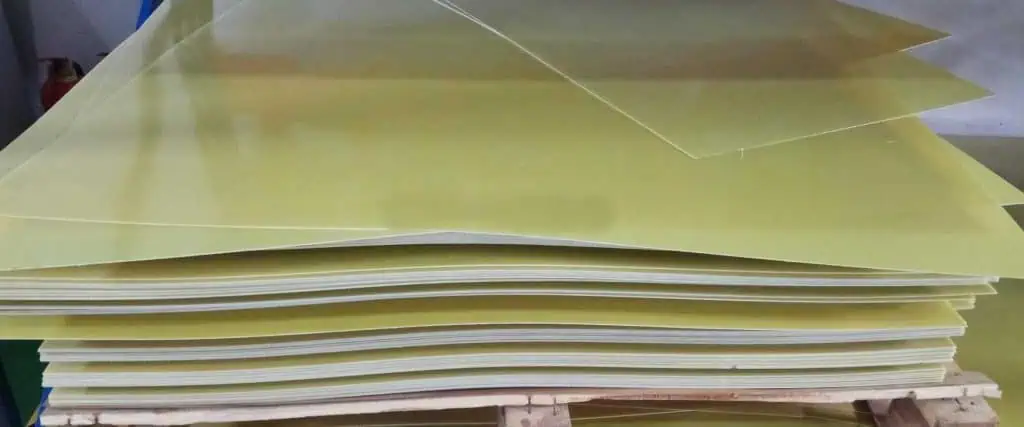
In contrast to the phenolic paper that emits brown color linked with the brown PCBs, the majority are constructed of glass fiber. This is so that glass fiber can be used, which is more economical and more durable.
Holes of circuit boards are frequently tinned by some manufacturers to prevent oxidation and facilitate soldering. The majority of universal PCBs include soldering pads for connecting components, however some also have the spring terminals that are more suitable to hobbyist projects than intricate designs.
Description of the Universal PCB
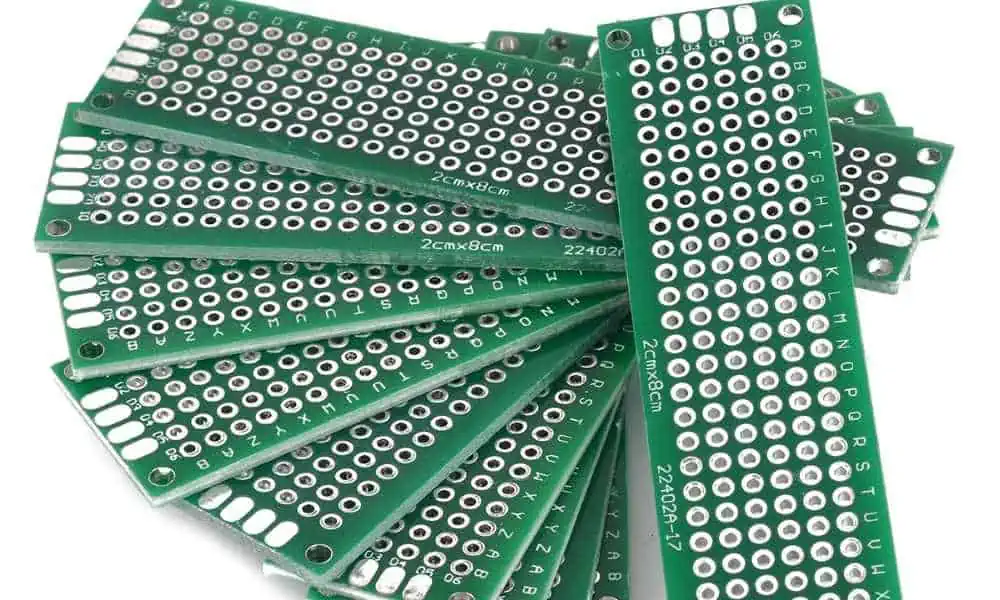
Universal PCBs come in a variety of forms, dimensions, and styles, ranging from large circuit boards having sides measuring a few dozen centimeters in length to the rectangular PCBs which are nearly postage stamp-sized.
There are also boards available in the shapes of the euro cards featuring edge connectors as well as spherical PCBs, that are designed for computer card prototypes and LED illumination, respectively. They come in single-sided as well as double-sided versions and are made of paper laminates and glass-epoxy laminates with a range of thicknesses between 0.7 and 1.6 mm.
Despite the market’s diversity, the majority of universal PCBs adhere to an unwritten industry standard regarding dimensions. The boards often come in a set of between five and ten pieces, with each measuring roughly 5 × 7 cm, and are typically double-sided when you buy them from websites. Typically, its thickness is 1.6mm. The length of each grid equals roughly 2.5 mm, while the diameter of each hole is roughly 1 mm.
Even with all the advantages that circuit board prototype universal pcbs have, when it involves mass production of any tried-and-true PCB concept, the discussion always returns to circuit boards. The large-scale production might not necessarily result from the case.
The current project might be small and only involve singular units. Nonetheless, the majority of electronic projects which require a general-purpose Circuit board for the prototyping seem to be near the conclusion of mass production.
As a result, using universal PCBs is much more temporary and using circuit boards that are well known is much more permanent. Now let’s talk about circuit boards as well as how they highlight prototyping’s beauty.
Which Types of PCBs are There?

One sided PCB
There is only one layer of base material or substrate on the one-sided PCB. On one end of the substrate, a thin metal layer, usually copper because it’s a good electrical conductor, can be applied. When a protecting solder mask often is placed on top of a copper layer’s peak, the finishing silkscreen coat might well be applied to the top to identify the board’s components.
This PCB has many circuits as well as electronic components on just one side. This type of module actually works for the simple circuits, thus beginners commonly design and build such a board initially.
Two-sided Board PCBs
In comparison to single-sided boards, this type of Pcbs is much more prevalent. Elements are connected to the two sides of the board’s substrate, which has some conductive layers of metal on both sides. Circuitry solely on a single side of the PCB can connect to circuitry located on the opposite side thanks to holes in the PCB.
Multilayer PCBs
These PCBs have extra layers coupled with the bottom and top layers present in the double-sided construction, which makes PCB designs more complicated and dense. With access to several layers in such arrangements, multilayer PCBs allows designers to produce exceedingly thick and intricate designs.
Power planes that serve as extra layers in the design, provide the power circuit supply while also lowering the levels of the electromagnetic interference which are emitted through designs.
Universal PCB Printing
Depending on what etching type is employed for PCB production, a circuit board’s materials and tools can differ dramatically. Yet regardless of whether etching can be carried out manually, with the aid of a machine, or using a chemical etching solution, there’s a standard tools set, which are useful, these include a printer and a PC.
Some supplies you’ll need include PCB boards that are photosensitive, transparent slides, cotton buds, Indian ink, paper towels, source of UV light, Drill bits, two glass or plastic bottles, two 1L bottles that are empty, rubber gloves, photosensitive circuit boards, fine sandpaper and perhaps kitchen scrubber, hydrochloric acid, acetone, thinner, and kitchen cleaner. Other items include copper boards, and hydrogen peroxide.
Depending on a number of variables, printing can use a variety of different procedures. Some methods include:
Acid Etching
The process employs a range of materials, such as the etchant, is quite slow, and therefore necessitates numerous safety measures. Depending on what materials you choose, the PCB’s quality you receive will vary, but broadly speaking, this is a decent solution for circuits having low to a medium degree of complexity.
Method of Routing
Specialized equipment which can mechanically eliminate extra copper out from board or install empty separators across wires is needed to use this procedure. One of these equipment can indeed be costly to buy, and renting it typically requires access to any nearby workshop. But, if you frequently need to duplicate your circuit and create high-quality PCBs, this approach is fantastic.
What are the Applications of the Universal PCBs?

Medical device
The healthcare sector uses PCBs more and more as technology advances and unveils new potential. A wide range of devices, such as those for therapy, monitoring, and diagnosis, make use of PCBs.
PCBs inside this industry frequently need to follow strict sanitary rules, especially during their implantation. Moreover, boards for a variety of applications, including ER monitoring, must be extremely small.
Consumer Electronics
PCBs are necessary for the operation of a wide variety of many other consumer goods. As more goods include electronics, Circuit boards become increasingly prevalent in our everyday lives. Small PCBs having a lot of connections are needed as manufacturers create smaller cellphones and laptops having improved capabilities.
To keep the price of consumer electronics low, PCBs must likewise be reasonably priced. Manufacturers also desire reliable boards because their ability to remain in business depends on the performance of their goods.
Industrial Equipment
The majority of the machinery in manufacturing as well as the distribution facilities, coupled with other industrial buildings, is powered by electronic components.
PCBs utilized in industrial sector typically need to be exceptionally powerful as well as long-lasting to withstand very harsh conditions present in industrial buildings.
PCBs must be protected from vibration, abrasion, extreme temperatures, as well as harsh chemicals when they are utilized in industry. Industrial PCBs might well be thicker compared to the other PCB types and made of materials which can endure high temperatures so as to meet this demand for durability. The industrial PCBA services may use through-hole technology to increase the strength of the boards.
Automobile Industry
Electronic components are being used in automobiles in increasing numbers. Originally restricted to headlight switches and windshield wipers, PCBs now offer a variety of cutting-edge technologies that improve safety and ease of use while driving.
Depending on its application, a PCB could need to tolerate extreme vibrations or temperatures. Additionally, it’s essential that they function reliably when they’re included in the car security feature. Manufacturers may use high-temperature laminate, copper or aluminum substrates, or thru-hole mounted components to address these problems. They also employ flexible stiff PCBs due to their resistance to vibration.
Ironing the Printed Universal PCB Layout
The schematic of the paper circuit and circuit board must be oriented. The schematic should be facing the circuit board’s copper portion. At this time, your iron ought to be on. Wait for the heating up of the iron after setting it to cotton setting.
The iron has to be heated up before being placed lightly on your paper top covering your circuit board. The iron must stay in position for about 30 to about 45 seconds. Carry the PCB to the closest water source after lifting the iron then carefully setting it aside. Avoid detaching the paper from the pcb board; it should be adhered to the board.
Hold your circuit board firmly down when the water begins to flow. After then, the paper would begin to gently and fully flake off. You could try soaking for a little bit longer when you find that some regions are particularly challenging to accomplish.
You should have the copper board having your PCB pads and signal traces etched out into a black toner if everything goes according to plan. Large water droplets could be easily removed by dripping them out or by gently wiping them off with a sponge or napkin.
Conclusion
Universal PCBs come in a variety of forms, dimensions, and styles. It also has countless uses and different applications.