DGP20E24T5/15 is a DGP20 series of DC DC Converters from the stable of Bel Power Solutions. The manufacturer made it into an isolated module; a module that further enhances the converter’s performance.
In this article, we will share with you, some of the important attributes of this DC DC Converter.
What is a DC DC Converter?
First, let us start with an understanding of how a DC DC Converter works. A DC DC Converter is a type of device used to change the direct current voltage input level of an Integrated Circuit (IC) into another that has a direct current voltage output level.
By making this change, it enables the converter to optimize the performance of the target applications or devices, as per the required levels (output or input).
DGP20E24T5/15 is based on the DGP20 series of DC DC Converters manufactured by Bel Power Solutions.
The DC DC Converters in this series are known for the following:
1. Extended Input Voltage
The DGP20 DC DC Converter series use an extended input voltage, with a ratio of 2:1. This allows for the extended or improved operations of the converter to interface with multiple resources. These varieties of resources can be anywhere between 9 and 72 volts.
2. The Tri-Output Design
DGP20E24T5/15’s architecture is based on a triple output model; a model that allows for the converter’s improved functions via the high-performance 20-watt triple output.
Considerations for the Performance
Although DGP20E24T5/15 is rated a high-performance DC DC Converter, it does rely on certain parameters to get to that level.
By default, it doesn’t necessarily need an external capacitance, but you want to consider that under a special circumstance.
If you are looking at getting the most maximum performance possible, it is worth it to use a capacitor with the DGP20E24T5/15. That way, you would be able to derive sufficient ripple current capacity, which is typically connected across the converter’s input pins.
Likewise, DGP20E24T5/15 doesn’t necessarily need an external output capacitance. However, considerations for this are to be made if there is a need to further reduce the system noise.
System Flexibility
DGP20E24T5/15 is one of the most flexible DC DC Converters you can come across. The system’s flexibility is derivable from the up to 11 watts of cubic inch for the power densities.
DGP20E24T5/15 supports noise reduction during operation. However, there is also a chance to further the reduction, especially along the lines of filtration.
To do that, an additional output capacitance is to be added to work alongside the existing 10µF of tantalum and up to 0.1µF of ceramic capacitance.
To that end, it is possible to add up to 400µF of additional tantalum, just to filter the noise further.
DGP20E24T5/15 has Remote Operation
DGP20E24T5/15 is a DC DC Converter with remote operation, especially for supporting the On and the Off operations.
The Remote ON/OFF operation is one of the key mechanisms in the converter’s low-power operation, as it can be used to switch the voltages. For example, the Remote ON/OFF operation/pin can be pulled down to the -INPUT to activate the low-power drain state.
While making the switch, make sure that the pin doesn’t have more than +8 volts or be above 0.3 volts below the -INPUT.
Technical Properties
Here are some of the technical properties or attributes of this DC DC Converter, as represented in a table:
An Isolated Module, according to DigiKey, helps in regulating the electrical separation of input and output voltages – which is what the DGP20E24T5/15 DC DC Converter does.
By creating the isolation, the isolated module helps to prevent the presence of a direct conduction path of metallic property between the two circuit parts (input and output).
Thus, if you are not sure of the relevance to the DGP20E24T5/15 DC DC Converter, here are some of the benefits:
3. Noise Segmentation
Although DGP20E24T5/15 uses an external output capacitance for noise filtration and reduction, it does have some other ways of getting around it.
The isolated module plays an important role in this regard, through the breaking up of the ground loops. This activity leads to the separation of the circuit parts that are more susceptible to noise.
4. DGP20E24T5/15’s Isolated Module Offers Different Levels of Isolation
The isolation of the input and the output voltages is the basic process. The isolated module also extends the isolation to the application’s protection, whereby it prevents the isolated circuit parts from posing danger.
For example, it has what is called the Reinforced Insulation. This type of insulation offers double protection for the isolated circuit parts.
There is the Operational or Functional Insulation; an isolated module that doesn’t offer shock protection, but makes up for that by offering operational security.
The Basic and Supplementary Insulation methods are also on the list. The former works by offering a single layer of insulation, which also offers shock protection. The latter, supplementary insulation, is ideal for adding more redundancy to the basic insulation model.
However, using the isolated module may come with some trade-offs, especially size-wise. The size of the module is higher than the other variant (the non-isolated module). Thus, it tends to take up more spaces in the target applications or circuit boards.
Conclusion
DGP20E24T5/15’s combination of the extended input voltage range and the high-performance, 20-watt triple output combine to give the converter a higher operating voltage.
Now that you know about some of the properties, make sure that the application or use case is either for telecom consumer electronics or battery-powered applications. That is because those two are the major use cases for the DGP20E24T5/15 DC DC Converter.
Consumer electronics are using memory to store information and to transmit the same. The EEPROM memory is one of the popular memory types. In this article, we discuss the workings of AT24CM02-SSHM-B, one of the popular EEPROM memories from Integrated Circuit (IC) manufacturer, Microchip Technology.
How Does an EEPROM Memory Work?
EEPROM is a format of semiconductor device, optimized for storing information/data on the Integrated Circuit (IC). It is a non-volatile memory designed to process data transfer via the I2C memory interface.
AT24CM02-SSHM-B’s Writing Operations and Error Detection Capabilities
Error detection is now an integral component or feature in most Integrated Circuits (ICs). AT24CM02-SSHM-B is not lagging in that respect, either. The built-in error detection capabilities interface with the writing operations.
First, let us talk about the writing operations. AT24CM02-SSHM-B uses a Start Condition, which the host uses to initiate a data transfer sequence. Upon the activation of the said condition, it would then be up to the built-in Error Detection and Correction (EDC) logic scheme to find the “faults.”
The EDC logic scheme then reads the 38-bit of Error Correction Codes (ECCs) in the EEPROM Array. By reading these codes, the EDC finds out if there is anything out of place by comparing the 6 ECC bits from the EEPROM with the four connected 8-bit bytes from the EEPROM Array.
The comparison reveals whether there has been any incorrect reading of any of the bytes from either section (the EEPROM Array and the EEPROM).
In the case of an incorrect data reading, what the Error Detection and Correction (EDC) logic does is to use a correct or updated value to replace the incorrect bit. That way, everything relating to the data would be uniform by the time it is serially clocked out.
AT24CM02-SSHM-B has Higher Data Reliability
Everything relating to data must not be treated with kid’s gloves, especially when it is used in consumer electronics. Microchip Technology, the manufacturer of AT24CM02-SSHM-B’s EEPROM Memory function takes that into consideration.
It maintains the highest data reliability standards by first using the endurance rating up to 1 million write cycles. It also keeps the data or information safe with the 100-year data retention.
The table below shows the different values making up the AT24CM02-SSHM-B EEPROM Memory:
Attributes
Description
Operating Temperature (minimum to maximum)
40-degree Celsius to 85-degree Celsius
Type of Memory
Non-volatile
Type of Package
Tube
Type of Case
8-SOIC
Technology Used
EEPROM
Clock Frequency
1 MHz
Memory Format
EEPROM
Voltage Supply (minimum to maximum)
Between 1.7 volts and 5.5 volts
Memory Interface
I2C
Estimated Write Cycle Time
10ms
Access Time
450 nanoseconds (ns)
AT24CM02-SSHM-B Pin Considerations
Pins play an essential role in the functions of an Integrated Circuit (IC). Careful considerations are to be made when working with these pins. AT24CM02-SSHM-B’s pins are important elements in the data writing capabilities.
Up to eight (8) different pins are supported, namely:
VCC
NC
WP
A2
SCL
GND
SDA
These pins cut across different ball compositions and functions, such as:
The Serial Clock (SCL) and the Serial Data (SDA) pins appear to share the same function, but there is a thin line differentiating one from the other.
On the one hand, SDA is an open-drain bidirectional Input and Output (I/O) pin meant to make serial transfer or movement of data to and from the (target) device.
On the other hand, the Serial Clock (SCL) provides a clock to the (target) device. The clock helps regulate the movement, transfer or flow of data to and from the (target) device.
Thus, the difference between the two is that despite aiding data transfer to and from the target device, the SDA differentiates from the SCL because it is an Input and Output (I/O) pin, while the latter provides a clock for the data transfer.
Device Address Input (A2)
This type of pin is used primarily for connecting two or more Serial EEPROM devices. For that to work, the Device Address Input (A2) is first hard-wired either to the VCC or to the GND pins.
Either way, the hard-wiring paves the way for the creation of compatible interfacing between the GND or the VCC pins with the additional two-wire Serial EEPROM devices. That way, multiple devices can be addressed or connected via a serial bus system.
Write-Protect (WP)
The Write-Protect or WP pin is used to enable the normal writing operations in the AT24CM02-SSHM-B EEPROM memory.
For the writing to be enabled, AT24CM02-SSHM-B is first connected to the Ground (GND) pin.
However, it provides protection for the data in the form of prohibited access. To enable this, the Write-Protect (WP) is connected directly to the Device Power Supply or VCC pin. By making this direct connection, Write-Protect (WP) prevents the memory from exposure, especially for the write operations.
How the VCC and the GND Pins Work in AT24CM02-SSHM-B
The remaining pins to analyze are the Ground (GND) and the Device Power Supply (VCC) pins.
They work together in the sense that the VCC is the major supply voltage to the device, while the GND serves as the “ground reference for the power supply.”
Data transfer is done via AT24CM02-SSHM-B’s I2C-compatible two-wire digital serial interface. Through this interface, the memory communicates or interfaces with the host controller. For emphasis, the host controller is the core initiator and manager of the client devices’ read and write operations.
It also oversees the enablement of the two-way data transfer process, allowing the client devices and the host (bus host) to transfer and receive data on the same bus.
The data transfer process typically involves the reception of the clock from the host through the Serial Clock (SCL). Once this has been done, the next stage would be the reception and transfer of the data information and command from the Serial Data (SDA) pin.
Conclusion
AT24CM02-SSHM-B is an excellent EEPROM memory required for surface-mounted devices needing excellent command and data transfer to and from the target devices/circuit boards.
Wearable technology is a hot topic in the tech world. These wearable devices are becoming more popular every day. There are many types of wearable technologies like smartwatches and glasses, which we can use for various purposes such as fitness tracking, communication, and data storage. These devices are also attached to our clothes and can be used for various activities like work, having a conversation, or even playing games. I have never met anyone who does not wear some type of smart device these days.
Many companies make smartwatches and other wearable technologies. Some people use them in their work while others do not have any reason why they should wear them unless they want to see the time on the watch or something like that. I am sure you will find out what you like. If you have a watch and do not need to see time, it is better to go for the chronograph watch as it will provide you with the best form of fashion in your life.
Wearable devices can provide many benefits to our lives, from improving our health to enhancing our safety and security. The technology behind these products has been around for many years and is increasingly progressing from simple consumer accessories to practical applications. For example, microchip implants in the United States replace passwords and keys and are implanted into fingertips via radio frequency identification (RFID). The technology also offers many practical uses, and RFID chips are under investigation for use in tracking the movement of US army troops throughout the world. In addition, specially designed wearable devices are under development by organizations like Rayming Technology for environmental monitoring, and Cyrcadia Health is developing an app to detect early signs of breast cancer.
A wearable device is any technology designed to be worn. Examples include smartwatches and smart glasses. This type of technology is a useful addition to our lives. For example, it helps us stay in touch with friends and family, keep track of our activity, and help us manage our health and weight.
We can use these devices to measure various health metrics, including your heart rate and blood glucose levels. Some of them don’t even require skin contact. They are extremely convenient and useful, but they also pose several risks. There is a risk of electro-sensitivity and EMF exposure from wearing devices that connect to the internet. Some people may experience ringing in the ears, unexplained hives, or chronic headaches. Other possible side effects include body pain and excessive fatigue. Wearable technologies can also be made of different materials that can cause allergies or other health problems. Another risk is an electrical shock if there is constant contact with the device. Faulty circuitry can be the cause.
Medical wearables are also becoming increasingly useful. In addition to letting people know how much exercise they’re doing, these devices can track biometrics in real-time. The technology is constantly evolving, and some companies are already working on diagnostic and treatment regimen wearables. Some devices can even be embedded into the skin. Others monitor vital signs, track prescription drugs, and test blood oxygen levels.
Wearable technology is a new trend that is growing in popularity every day. It has the potential to revolutionize how we work and live. Wearable devices are increasingly becoming a part of our daily lives. They have become more affordable and more convenient to use. They can be useful for a variety of purposes, such as:
Personal fitness tracker
Activity monitor
Sports watch
Smartwatch
Smart glasses
Fitness tracker with GPS and heart rate monitor, etc.
In a world where smartphones have taken over, wearable devices are changing our lives. There are many health segments in which wearable devices can help you achieve your fitness goals. This includes walking, running, cycling and swimming. They were also very useful in making fitness plans in previous times as well. The latest version of Fitbit has been launched to provide a range of new features to users and make it reach more people interested in wearing these devices on their wrists or around their necks to stay fit.
We can even use them as a replacement for smartphones in some cases because they provide us with much more functionality in the same price range (less than $100). The best part is that they are also very easy to use and can be used by anyone regardless of their technical knowledge or expertise in this specific area. In addition, they are not complicated to set up or learn how to use, so you don’t need any kind of special training or experience just to start using them immediately. You can buy these devices from many different online retailers, like Amazon, Walmart, Best Buy, etc.
Growth of the Wearable Industry
The wearable technology industry has various applications, from consumer electronics to professional sports. It is becoming increasingly more sophisticated and capable of incorporating human-machine interaction into everyday activities. Several notable use cases include fitness trackers, smart watches, smart clothing, and navigation systems. These innovations are also useful in professional sports and healthcare.
In sports, wearables can monitor a range of vitals, from heart rate to calorie intake. Some are even designed to track training regimens. Moreover, recent health concerns, including the COVID-19 pandemic, have led to increased use of wearable technology. They can also help monitor the spread of infection and improve personal hygiene.
The development of wearable technology has a long history. Its earliest forms date back to the invention of glasses, developed more than 800 years ago. Another early wearable technology was the wristwatch, which evolved from large clocks. The modern-day wearable industry began in the 1950s, but the original devices were not at all what they are today.
These devices are becoming more sophisticated and can now detect complex human physiology data. These wearables can even detect the effects of stress, which is a major cause of many health problems.
Wearable technology has also made a huge impact on the business world. Today, 79 percent of employees are wearing smart devices in the workplace, and 82 percent of them report using the device to enhance their work. The technology can improve communication, track employee activity, and improve job site safety. It can also improve an employee’s quality of life and increase retention and productivity.
Wearable technology has several different uses. Some are medical; others are entertainment and gaming. It can encourage healthier lifestyles and enhance physical performance. Many industries have welcomed this, including healthcare, sports, and insurance. For example, the healthcare industry has seen many benefits from wearable technology.
Similarly, manufacturers of sports equipment have embraced the technology. In the late nineteenth century, the wristwatch became popular as a wearable version of the pocket watch. In the twenty-first century, smartwatches and smartphones have evolved from pocket-sized devices to being worn on the wrist.
Sports and Fitness
Wearable technology has the potential to improve sporting performances in many ways. For example, it can monitor various parameters, such as heart rate, blood pressure, and oxygen enrichment, and alert medical personnel to possible injuries. These devices are already being used to monitor the performance of athletes and track their progress throughout the game.
Although these technologies are powerful tools for health and fitness, they are not without limitations. These limitations are largely related to reliability and validity. While the rapid development of wearable devices may lead users to believe that their accuracy is unquestionable, published research suggests that such devices are valid only in a limited number of circumstances. Further, they are best in the context of the low-intensity activity or when the user does not use a lot of energy.
The popularity of wearable technology in sports and fitness is growing. The technology is being marketed to the general public and elite athletes. This new technology has the potential to have a significant impact on cardiovascular health, physical activity, and mortality risk. It is also a great way to keep track of your sleep patterns and overall physical activity.
Military
As the world continues to face asymmetric warfare, wearable technology is finding new applications for the military. With the help of technology, soldiers can wear medical equipment, keep track of their fitness levels, and even monitor the environment around them. This technology will be beneficial to both soldiers and combat arms.
Military wearables will improve the performance of soldiers and help prevent injuries. They will also help to optimize the combat capabilities of a joint force. These technologies will be customized for each soldier, ensuring they get the most out of them. In addition, these devices will provide real-time recovery predictions and secure data transfer methods.
Building a robust network infrastructure along the border will be critical in bringing wearable technology to the battlefield. Reliable backbone fiber connectivity is a must. In addition, you can terminate wireless networks on fiber networks for last-mile connectivity. Another important step is combining implantable sensor technology and the Internet of Battlefield Things. This can make battlefield management entirely digital.
Wearable technology is a hot topic these days, with many different applications. One example is smart wear. These garments use thermal energy to recharge a smartphone or a tablet. Another is augmented reality. This technology lets people explore landmarks with a few clicks of their wrists.
This type of wearable technology is also useful for health-conscious people. A wearable device can improve the balance of physical activity, nutrition, and well-being. We can apply such in serious gaming. For example, a wearable device that monitors your heart rate can be a motivational tool.
Medical and Health Monitoring
Wearable technology is changing the way healthcare providers monitor patients. Using sensors embedded in clothing, eyeglasses, gloves, and other wearables, healthcare providers can monitor patient health data and adjust treatment plans when necessary. This can be very helpful for patients with certain conditions and reduce staff workload.
Wearable devices record biometric data and can help diagnose illnesses early. They can detect symptoms and measure blood pressure or heart rate. Using light-based sensors, they generate biometrics, which can be useful for determining health problems and detecting abnormalities. Wearable devices also provide insight into physiological systems, which can lead to improved treatment options. Approximately 85% of healthcare costs are related to chronic illnesses, so this technology can be a great ambulatory solution for monitoring physiological parameters.
Wearable technology is also helpful for preventing diseases. The use of health monitors helps detect symptoms early and encourages healthier lifestyles. In addition, these devices help patients compare their results to goals, and they can track progress against those goals. With the help of modern technology, healthcare providers can monitor patients around the clock, identifying early signs of serious illnesses and offering preventive care.
Fashion and smart clothing uses of wearable technology are emerging, and consumers have a mixed reactions. The rejection of smart clothing is often due to a lack of consumer understanding or an unwillingness to invest in new products. However, it does not necessarily mean that consumers will not adopt new products if the design is not appealing. This study used a preliminary interview to gather data on consumer perceptions of smart clothing and then conducted in-depth interviews with 30 consumers from different demographics. The research focused on consumer attitudes, preferences, and opinions about smart clothing and whether or not they would purchase the product.
The development of smart clothing is a complex process. First, designers must ensure the clothing is practical and attractive and should consider the characteristics of consumers. For example, color choice must take into account the age group of the target consumer. Older consumers will want to wear conservative, muted colors, while the young prefer vibrant ones. In addition, children’s clothing should be designed to focus on novelty and fun. While wearing smart clothing, however, designers must consider the concealment of electronic components.
Although most developments of smart clothing are still taking place in research labs, there are several examples of the integration of wearable technology into clothing. For example, Levis recently introduced a denim trucker jacket with Google software. This jacket allows users to read messages, respond to notifications, and play music. These devices target urban cyclists, but smart clothing can be useful for various purposes.
Performance monitoring and navigation tracking
Wearable technologies provide information about human performance by collecting various metrics. These metrics can be based on running speed, the inclination of the terrain, and heart rate. Some wearable devices are capable of estimating the workload based on these metrics. These devices are suitable for both ambulatory and clinical settings.
Wearable technologies can be worn on the body or embedded within clothing or other semi-rigid structures. These devices can communicate through the human body using appropriate transmission mediums, such as BLE, Wi-Fi, and cellular data. You can store the collected data from wearable devices for long-term analysis. The devices may not process the data locally but instead, send it to a remote computer equipped with powerful processing capabilities.
Wearable technology is gaining popularity in both elite and general populations. Its widespread use in the health and fitness industry has led to significant growth in the market. A recent study examined the effectiveness of five wrist-worn devices against a respiratory gas analysis method. The authors found that most of these devices had a mean absolute percentage error greater than 10% and often underestimated the amount of oxygen a person is breathing. Nevertheless, this study highlighted the potential benefits of wearable technology for health and fitness.
PCB manufacturing and assembly services
The PCB manufacturing and assembly services for wearable technologies require extreme precision and close attention to detail. In addition, this technology requires circuits that can function in extreme temperatures and environments. For example, a wearable device may be necessary to function properly in a harsh winter in Moscow or a sweltering summer in Mesa, Arizona.
PCBs are present in many medical devices, including implantable defibrillators and cochlear implants, which help the deaf process sounds. Implanted defibrillators help protect people at risk of cardiac problems. And wearable technology includes devices like the responsive neurostimulator, which monitors brain activity around the clock.
PCB manufacturing and assembly services for wearable tech require that you submit your design files to a contract manufacturer. The contract manufacturer will provide the SMT stencil, PCB boards, and other components needed for assembly. PCB assembly companies can provide parts sourced from their established relationships with suppliers and can save assembly costs by purchasing parts in assembly-friendly packages.
The PCBs used in wearable technology are typically smaller in size than the average PCB. However, the smaller PCBs require a lot of precision. As a result, EMS providers should be ready for this new level of complexity.
Wearable tech can take many forms, from jewelry and accessories to medical devices and clothing. This technology is designed to use electronic components worn on the body and has processing and communications capabilities. Some of the most advanced wearable techs include artificial intelligence hearing aids and holographic computers in VR headsets. Others include fitness trackers that record steps taken and play music through a cellphone app.
The military uses wearables to monitor soldiers’ vital signs and performance. Similarly, sports wearables are embedded in athletic apparel and equipment, relaying real-time data to coaches and players. They also use Bluetooth technology to track player health and performance metrics. Wearable tech is also useful for people in remote locations without internet access.
Wearable tech has many applications and is becoming a functional part of our everyday lives. This technology allows us to be hands-free when performing routine tasks, including tracking emergency response teams. It can also collect data for digital management. Smart glasses and watches are two common examples of wearable tech.
While many wearables attach to clothing, some are completely separate. For example, smart glasses and smart clothes allow people to monitor their health and activities. Smart jewelry is another form of wearable tech. It allows people to answer calls through the sleeve without the need for a phone.
Wearable technology is becoming more popular, especially in the gaming world. Many types of wearable technology are available, but one of the most exciting is VR headsets. There are also many different types of fitness devices and smart clothing available. All of these devices are just the tip of the iceberg.
Even though there are many innovations in wearable tech, many people still fear being tracked and hacked by malicious devices.
The Importance of Good Electronic Contract Manufacturers in the Wearable Industry
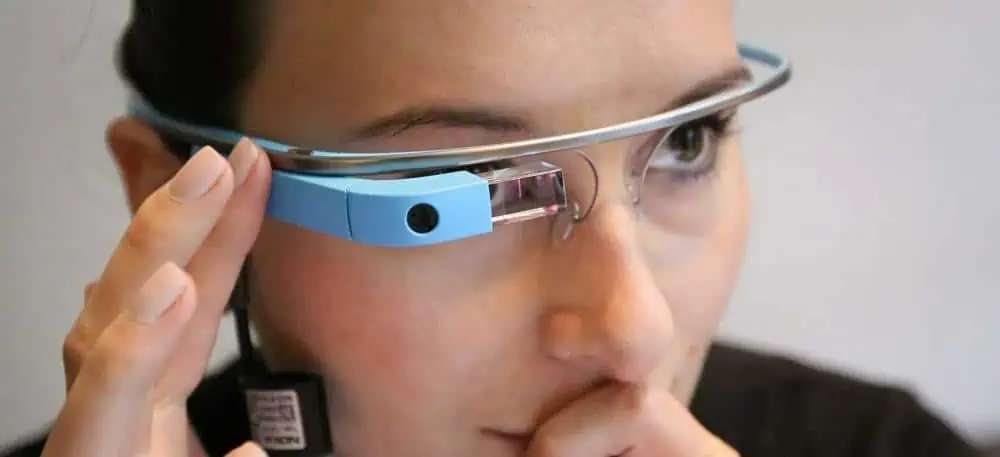
eye glasses wearable devices
The current market environment is one of the most competitive in the industry. A company can compete with its competitors by providing the right product.
We should not consider these electronic contract manufacturers as replacements for human manufacturers. Instead, they just assist their clients by ensuring that their products are delivered on time, on budget, and at a reasonable cost.
There are a lot of manufacturers that produce electronic contracts. But there are also a lot of companies that manufacture electronic contract software. And there are also a lot of companies that specialize in manufacturing physical contract hardware such as smartwatches, fitness trackers, and other wearable devices.
And this is where Rayming PCB & Assembly Company comes in. Rayming Technology Company is an ISO 9001:2008 certified manufacturing company offering custom-made PCB designs, assembly, and testing. It can provide a 24-hour turn-around service by providing the design from CAD layout to the completed board. Independent third-party certifications have validated the company’s components for quality and safety. Their products have a 100% lifetime warranty against all defects in construction and materials. The company offers professional services such as design development, quality control, materials selection & testing, installation, transportation, and delivery. They use high-quality materials to achieve exceptional results. These tools can effectively protect your investment in quality timepieces for generations to come.
PCB manufacturing and assembly services
A PCB assembly service can provide the required parts for your wearable device while you focus on developing the wearable device. Full turnkey PCB assembly services will require you to send your design files to the contract manufacturer, who will then provide the PCB boards, SMT stencil, and parts required on the bill of materials (BOM). These PCB assembly services will include procurement and assembly, and most contract manufacturers have excellent relationships with their parts suppliers. As a result, the parts are purchased in packages that are assembly friendly, saving you money and time during the assembly process.
PCB assembly services can also address safety concerns, such as maintaining cleanliness. A PCB manufacturer that specializes in medical devices will be able to design the PCB for the device following the required standards and will address any concerns you have about the device’s performance. Additionally, medical PCB assembly services can make sure that your device is designed to be quick and precise.
A PCB that meets the needs of wearable devices is typically very small, requiring careful component selection. In addition, because wearable devices have different requirements than other devices, PCB manufacturers need to ensure that they are ready for the new demands. Hiring a qualified EMS provider will help you increase the chances of a successful PCB assembly.
Medical PCB assembly services are essential for several medical devices. From wearable devices to personal health monitors, PCB assembly services help manufacture the devices that help save and enhance patients’ lives. For example, PCBs are crucial in the design of cochlear implants, which help the deafened heartbeat of patients. Also, implanted defibrillators are critical for people at risk of cardiac problems. Finally, a PCB for a responsive neurostimulator can monitor brain activity around the clock.
The PCB manufacturing and assembly services for wearable electronics require extra care and attention to detail, especially with small components. In addition, these PCBs must operate reliably in extreme environments, be it winter in Moscow or summer in Mesa, Arizona. These new requirements for wearable electronics require new skills and technologies, and the right EMS provider can help you meet these challenges.
The PCB assembly process is critical for the manufacturing of many medical devices. Today, PCBs are useful in various applications, from hearing aids for the deaf and hard-of-hearing, to implanted defibrillators that protect people at risk of cardiac failure. PCBs can also be used to make a responsive neurostimulator, which monitors brain activity around the clock.
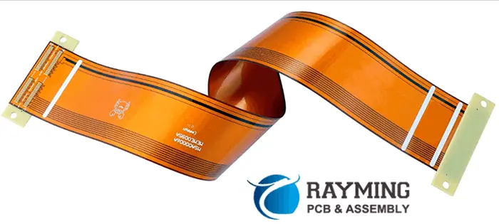
Wearable PCBs are often made using flex PCB technology, a type of flexible PCB used in many medical devices. These PCBs have a low ripple effect that reduces system noise and are compact. These PCBs also enable clean signal transmission. However, one of the biggest challenges in the PCB manufacturing process for wearable devices is dielectric constant tolerance. Many devices require a +2% tolerance, but some require a higher one.
PCB manufacturing services for wearable devices are becoming increasingly important as technology improves. These devices are becoming compact, fast, and stylish and should follow strict standards during manufacture.
Wearable devices and PCB manufacturers
Wearable PCB manufacturers face numerous challenges in designing the electronics that go into such devices. The primary constraints are the reduced footprints and low-profile packages. The circuit boards used in these products must be moisture-proof, and the materials used should be durable and reliable. PCBs manufactured for wearable devices must comply with safety and quality standards.
Wearable PCBs can range in structure from two to eight layers, with two to four being the most popular. However, when creating a PCB for a wearable device, it is crucial to use a multilayer structure to minimize electromagnetic interference and crosstalk. Additionally, wearable PCBs can include a ground plane between power and signal planes. This prevents crosstalk and enhances electromagnetic compatibility.
The manufacture of PCBs for wearable devices should use advanced technologies that can handle the high-performance demands of these devices. The materials used should have a minimum solution thickness and exhibit low laminate loss. Wearable PCBs are typically small-sized and can be as small as the size of a penny.
An electronic contract manufacturer is a manufacturer that produces electronic devices for a variety of markets. These companies may specialize in certain fields, such as medical devices, or they may have a wide range of capabilities. Choosing the right manufacturer is important because it will allow you to reduce production costs while receiving the highest quality products possible.
In addition to quality, you’ll want to look for speed and cost. Strong contractors will have quality assurance measures and documentation to prove their capabilities. You’ll also want to find out how well they know the materials and equipment that they use. In addition to that, ask about their turnaround time and value-added services, such as sourcing raw materials.
To be successful in this market, an EMS company must be able to meet the needs of OEMs. As a result, it must be flexible enough to provide solutions for niche products. For example, wearable devices and app-based devices have very specific requirements. In addition, engineers are increasingly using flex circuits. However, not all MDM designers understand how to properly design these circuits.
How to Choose the Right Wearable Device For The Job & Beyond
Wearables are becoming a very important part of our lives. They can help us to do things like communicate with others, manage our health and fitness, and even perform tasks that weren’t possible before. They can be good for everything from sports to medicine and even entertainment purposes. So it’s natural that you want to ensure that your device is the best. The best part about wearing a wearable is its simplicity. You don’t need any special training or knowledge to use it. Simply put on the fitness band, start exercising, and then check your stats afterward to see how well you did compared to others.
You should consider:
The amount your willing to pay
The purpose for the wearable. Is it for notifications, tracking activity or answering emails/texts
Wearable devices and circuit boards are the bellwethers of what the rest of the electronics industry is producing. They are rapidly transforming our lives, especially through medical devices. So now more than ever, manufacturing companies need a specialist in the field who can provide reliable information when developing these technologies.
Rayming Technology will help you be successful in this market. Their consultants can help you decide which will work best for your company, especially as more wearable electronic devices become available on the market. As an EMS provider, they provide a range of solutions for these products.
Contact them today to learn more about their services. They can help you select the right technology for your wearable devices.
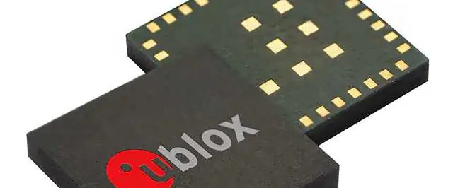
Ever wondered how an RF Receiver works? More especially, how the EVA-M8M-0-10 works as an RF Receiver? We are going to talk exclusively about all that in this article.
But before we proceed, we are going to talk about some of the things you need to know about this device. First, EVA-M8M-0-10 is an RF Receiver and it is primarily used with devices or applications requiring a modulated radio frequency.
When we are talking about these applications, we are specially mentioning the likes of USB, UART, Pads for Pins and Solder Pads. EVA-M8M-0-10’s RF Receiver is also used with I2C, I2S, Serial Interfaces and Parallel Interfaces.
With that being said, let us dive right into the article and talk about other things you need to know about the EVA-M8M-0-10.
Like most RF Receivers out there, EVA-M8M-0-10 works by taking in a modulated radio frequency. Once the frequency is taking in, it demodulates the radio frequency before passing the obtained data along for onward processing inside the system.
u-blox manufactures this EVA-M8M-0-10 and made it available for a wide range of applications, including but not limited to data-logging and space-sensitive applications. The idea is that can be used for a variety of purposes or applications, because it is a general-purpose RF Receiver.
EVA-M8M-0-10’s GNSS Module
EVA-M8M-0-10 uses the GNSS Module or protocol, alongside other modulations like GPS, BeiDou and GLONASS.
What is a GNSS Module and what role does it play in the EVA-M8M-0-10 RF Receiver? The full name is Global Navigation Satellite System (GNSS). It is a type of device used to form a constellation of the different satellites that provide signals from space. These signals are then pushed to or transmitted to the GNSS receivers; providing a combination of timing data and positioning in the process.
In terms of the EVA-M8M-0-10 RF Receiver, the GNSS Module aids in the simultaneous acquisition and capture/obtaining of the multiple satellite constellations. These would then be used for navigation, positioning and tracking applications.
As a general-purpose RF Receiver, the applications or use cases can also be extended to the space-centric applications.
1. Concurrent GNSS Module
Agreed, EVA-M8M-0-10 uses a GNSS Module, but there is another upside to it – it is concurrent. The concurrency of the module delivers the highest accuracy while ensuring that the processes are seamless.
It is worth pointing out that the GNSS Module relies on some of the best component-parts, including but not limited to BeiDou, GPS, GLONASS, and Galileo.
Although the GNSS Module makes up for most part of the signal obtaining and delivery, a lot still relies on other peripherals. It is in light of it that the several interfaces provisioned on EVA-M8M-0-10 come in handy.
For one, these interfaces combine to deliver the highest signal delivery possible. While the embedded firmware is primarily used for protocol-based specifications/applications, the others are used for memory, and data communication purposes.
This is a breakdown of how each of the interface work:
2. Interface Selection (D_SEL)
This is a dedicated interface for interfacing or choosing the best communication medium. When the D_SEL interface is activated, it can choose among the GND, DDC and UART interfaces for the communication.
For example, the GND interface is selected after the D _SEL pin has been set to the logical “0”. The setting permits the Ground (GND) interface to become the default communication interface.
Otherwise, the D_SEL pin can be set to the logical “1” to enable the duo of the DDC and UART interfaces to be used as the default communication interfaces.
3. UART Interface
Although it is used in the former reference for communication interfacing, the use case of the UART interface is primarily for communication. In this case, it has to be configured to support the configurable baud rates, as that is the basis for the usage as a communication interface to the host.
4. Serial Quad Interface (SQI)
This type of interface is used when looking to connect (multiple) interfaces to the EVA-M8M-0-10 RF Receiver.
How it works? It uses an optional external flash memory to make the connection. The memory referenced now can also be used for other purposes, ranging from data logging and making updates to the firmware.
5. Power Mode
EVA-M8M-0-10 uses a power-optimized architecture, which offers the best power performance, while cutting down (excessive) power, where possible.
To get the best power performance, EVA-M8M-0-10 has been optimized to work with multiple modes, such as the Power Save Mode and the Continuous Mode.
If you are working with the Power Save Mode, the use case is mainly to optimize the RF Receiver for the lowest power usage. On the other hand, you can activate the Continuous Mode if you are looking to get a mix of balanced power and low-power optimizations.
Consumer electronics now have several integrated components, including RF Receivers. EVA-M8M-0-10 is not an exception.
The ease-of-integration is drawn from the QFN-like package/case, which allows for the flexible integration in a wide range of devices.
Most importantly, the package allows for the production and availability of the GNSS Modules in both 500 reels and pieces. That way, it becomes easier to integrate the receiver into the target applications – especially in the small form-factor devices.
7. EVA-M8M-0-10 is a Product-Diverse RF Receiver
The general-purpose optimization aside, EVA-M8M-0-10 is also ideal for several use cases, thanks to the product diversity. The diversity in this case refers to the optimization of the receiver to work across different facets. It is also because of the following considerations:
8. Excellent Timing Solutions
EVA-M8M-0-10’s GNSS Module solutions support the configuration of applications or devices with a focus on precise timing, standard precision, dead reckoning and high precision solutions.
9. Customized Solutions
u-blox, EVA-M8M-0-10’s manufacturer, uses the “silicon,” thus making the general-purpose applications’ support more impressive. By using the company’s exclusive architecture, there is every assurance that stabilized product life cycles, controlled quality, excellent customer support and the highest performances are assured.
Conclusion
To sum it up, EVA-M8M-0-10 is a high-precision, optimized-cost and easily integrable RF Receiver for general-purpose applications.
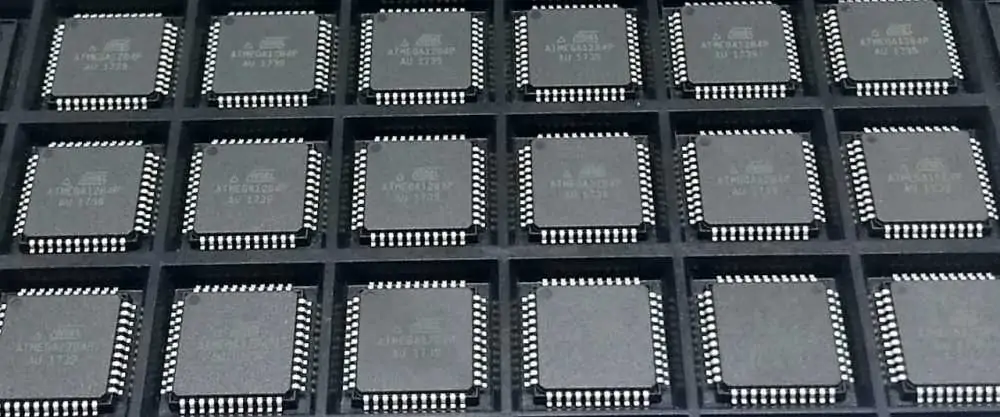
ATMEGA1284P-AU uses an AVR-enhanced RISC architecture combined with the 1 Million Instructions Per Second (MIPS) per Megahertz (MHz) to balance the power consumption with the processing speed.
We have made this blog post to help you understand how the ATMEGA1284P-AU Microcontroller (MCU) works.
The MIPS Architecture
MIPS stands for Million Instructions Per Second (MIPS). Essentially, it refers to the number or volume of instructions that can be processed with the ATMEGA1284P-AU Microcontroller. Like every other Microcontroller, ATMEGA1284P-AU works by storing data inside the circuit board.
By processing up to 1 million instructions per Megahertz (MHz), it sure is the go-to MCU for faster transactions.
Interestingly, not all Microcontrollers (MCUs) balance the performance with the processing speed. That is one feature that sets ATMEGA1284P-AU apart from the others – it balances processing speed with power consumption, through the MIPS.
ATMEGA1284P-AU uses some of the best peripherals you can find out there. From the PWM to the Brown-out Detector, it uses most of these peripherals to deliver the best performances.
Below is a breakdown of how each of the peripheral works:
PWM Channels
PWM stands for Pulse Width Modulation. According to Wikipedia, it is a “method of reducing the average power delivered by an electrical signal.” The average power reduction is facilitated by the bit-by-bit segmentation of the signals, typically into discreet parts.
Pulse Width Modulation performs many functions, ranging from voltage regulation, and controlling the amount of power delivered to a load. In this regard, the power delivery is done in a way that it doesn’t trigger voltage issues resulting from the delivery of linear power through resistive means/channels.
ATMEGA1284P-AU’s memory segments are not only non-volatile, but also have one of the highest levels of endurances.
The following are some of the attributes in that regard:
Programming Lock
ATMEGA1284P-AU protects the software through the Programming Lock feature.
Boot Code Selection
ATMEGA1284P-AU allows for an optional selection of the boot code, especially if independent lock bits are to be used.
The attributes in this regard include a True Read-While-Write Operation and an In-System Programming via the On-Chip Boot Program.
Data Retention Capabilities
The internal data storage function of a Microcontroller (MCU) helps to protect the circuit board against losing most of the configurations.
For that purpose, digital circuit designers look for the MCU with the best-possible data retention capabilities.
ATMEGA1284P-AU’s data retention capability is enabled through the high endurance, non-volatile memory segments. It can retain data for 20 years at 85˚C or for 100 years at 25˚C.
QTouch Library Support
Digital circuit designers looking to use the ATMEGA1284P-AU Microcontroller (MCU) are further empowered by the QTouch Library.
It is a dedicated platform for getting royalty-free software needed for configuring the ATMEGA1284P-AU MCU. The library comprises both the IAR and GCC; both used for developing the “touch applications” based on the Microchip AVR Microcontrollers (MCUs) and the AT91SAM standard.
The supported QTouch Library also includes support for up to 64 sense channels and the combination of capacitive touch buttons, wheels and sliders.
Besides the data retention, lowered power consumption and the support for the QTouch Library; ATMEGA1284P-AU also offers some other attributes.
Called the special microcontroller features, they are dedicated attributes offered for special purposes or functions.
The following are some of the special features:
1. Programmable Brown-Out Detection
Also called the BOD, the Brown-Out Detection is a dedicated facility inside a Microcontroller (MCU), serving the purpose of monitoring the dip or a drop in the MCU’s voltage supply.
Super User noted that a voltage is considered to be in an undervoltage condition, when the Alternating Current (AC) drops below the nominal or predefined below. In most case, the drop is highlighted when there is a 10% drop below the predefined value.
So, what the Brown-Out Detection (BOD) does in the ATMEGA1284P-AU MCU is to find out when this nominal value drops. It is also programmable, meaning that it can be configured to meet different applications’ requirements.
2. Internal Calibrated RC Oscillator
Oscillators are popularly used in Microcontrollers (MCUs), but that of ATMEGA1284P-AU is based on the Internal Calibrated RC design. According to the manufacturer, Microchip Technology, this type of oscillator is delegated when the internal RC oscillator is to be used as the CPU clock source.
3. Support for Several Sleep Modes
The ATMEGA1284P-AU is “put to sleep” when not in use. However, putting it to sleep might cause most of the components to stop working for the time being. This can, however, be tackled with the multiple sleep modes it provides.
Choices can be made from any of the following:
Extended standby mode
Idle sleep mode
Standby mode
ADC noise reduction mode
Power-down mode
Power-save mode
Each of those modes can be further programmed to adapt to the target applications’ power-saving requirements.
ATMEGA1284P-AU uses a programmable watchdog timer. A watchdog timer is the dedicated timer monitoring the operations of a Microcontroller (MCU), just to find out if the MCU is operating normally or not.
Therefore, it is to be regarded as the “watcher” that “keeps an eye on” the Microcontroller (MCU)’s operations.
ATMEGA1284P-AU’s watchdog timer is not just programmable, but also comes with the separated on-chip oscillator.
Here are some of the attributes making up ATMEGA1284P-AU’s programmable watchdog timer:
Selectable Time-Out
Due to the configuration for fault or abnormal operation detection, the watchdog timer might be unable to give the Microcontroller (MCU) the space to function beyond a lapse.
That informs the reason behind the integration of a programmable feature called the selectable time-out function on ATMEGA1284P-AU’s watchdog timer. It offers up to 16ms to 8s of timeout; giving the MCU some time to recover after a lapse.
Hardware Fusion
ATMEGA1284P-AU’s watchdog time also has a possible hardware fuse Watchdog Always on (WDTON) function. It works best for the fail-safe mode.
The other attributes of the watchdog timer are:
Interrupt and system reset
Interrupt mode
System reset mode
Final Words
ATMEGA1284P-AU regulates power consumption to the barest minimum, keeps the MCU active through the programmable watchdog timer and regulates electrical signal transmission via the Pulse Width Modulation (PWM) function.
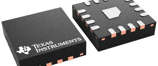
DAC80508ZRTET is a Digital-to-Analog Converter (DAC) with support for the buffered-voltage-output. Manufactured by Texas Instruments, it is the ideal DAC for low-power applications.
Perhaps, one of the most outstanding features is the composition of a 2.5-volt, 5-ppm/˚C internal reference; a composition that eradicates the need for an external precise reference.
The DAC Family
DAC80508ZRTET belongs to the broader DAC80508 family of Digital-to-Analog Converters (DACs). This family of DACs is reputed for the optimization for low-power applications.
By this classification, DAC80508ZRTET also offers a balanced power for the DAC outputs via the power-on-reset circuit.
If you are looking for a DAC with the most-minimized real estate, DAC80508ZRTET has to be on the list.
It supports form-factors, through the availability in smaller packages. For one, it is available in the 16-pin WQFN package with a body size of 3.00 mm by 3.00 mm. It is also available in the 16-pin DSBGA small package, with a body size (NOM) of 2.40 mm by 2.40 mm.
The small package optimization makes it ideal for the following applications:
Data Acquisition Systems (DAS)
Optical networking applications
Industrial automation devices
Wireless infrastructure
The Low-Power Design
DAC80508ZRTET is one of those Digital-to-Analog Converters (DACs) with a premium placed on power optimization. The low-power design is based on the use of the low-power 0.6 mA/Channel, which operates at 5.5 volts.
To that end, it offers an integrated power-on-reset circuit, which aids the power up or booting of the DAC, especially in the absence of midscale or zero scale. In that light, you can rely on it to maintain the base outputs of the DAC, and hold the same until a valid code is written to the target device or application.
The low-power channel is just a tip of how it is low-powered. The other aesthetics include the per-channel power-down function. This function is responsible for reducing the device’s power consumption to the barest minimum of 15 µA.
The operation of the 0.6 mA per channel is also a great customization that makes DAC80508ZRTET an ideal DAC for the battery-operated devices or applications.
DAC80508ZRTET’s internal reference paves the way for the DAC to expunge the need for external, precision interfaces.
At the core of the internal reference’s functionality is the low drift operation with a typical 2 ppm/˚C. It also features an initial accuracy of ±5 mV maximum.
Flexible Interfaces
The flexibility of an Integrated Circuit (IC)’s interfaces can make or mar the functionalities. DAC80508ZRTET’s interfaces are flexible as they allow for the customization and or further optimization of the DAC.
The flexible interfaces enable the operation or functioning of the DAC, as per the industry-standards for both Microcontrollers and Microprocessors.
To get an idea of the customization, its serial interface operates up to 50 Megahertz (MHz) of clock rates and a serial interface operation of 5.5 volts (maximum) via the VIO pin.
The flexibility of the peripherals is not limited to the interfaces, as DAC80508ZRTET is flexible with the output configurations. The configurations here include:
A clear output function
User Selectable Gain of ½, 1 and 2.
The DAC80508ZRTET DAC can be reset to either the midscale or the zero scales.
Digital-to-Analog Converters (DACs) pave the way for the conversion of transmission of a digital data or signal to a corresponding audio signal or data. Ordinarily, a digital data cannot take the place of an audio data because the two aren’t the same – and vice-versa.
Through the Digital-to-Audio Converter (DAC), it becomes possible to convert or make a digital data stream into an analog audio signal or data stream.
Here are some of the benefits to leveraging DAC80508ZRTET’s DAC:
1. Limited Noise
DAC80508ZRTET’s DAC doesn’t generate much noise because of the thermal noise design created by the passive components, including resistors.
The thermal noise design makes DAC80508ZRTET’s operation seamless, as it can potentially cut down the noise to less than 21 bits. From the information in the datasheet, the noise level is rated as 16-bits.
2. The Buffered-Voltage-Output Design
DAC80508ZRTET’s buffered-voltage is based on the Digital Buffer, which Wikipedia describes as an “electronic circuit element used to isolate an input from an output.”
The isolation keeps the different elements (input and output) independent and fully operation. Wikipedia also confirms that the digital buffer doesn’t necessarily have to make changes to the original state of the input and the output, because it allows the two to work in isolation without attenuation or amplification.
The buffered-voltage-output design in the DAC80508ZRTET is ideal for increasing the DAC’s maximum output range from 0 V to VDD.
In addition to the load-driving potential of up to 2 kΩ, the buffered-voltage-output also makes the driven load to be parallel to the 10 nF to Ground (GND).
3. DAC80508ZRTET Supports Wide Operation
Not all DACs support a broader operation, but there is an exception with DAC80508ZRTET. It supports a wide range of operations, including an operating temperature up to 125˚C.
Factors to Consider when Choosing a (DAC80508ZRTET) DAC
With the several functions it performs, it is not a doubt that DAC80508ZRTET is one of the best Digital-to-Analog Converters (DACs) to buy.
But it is not better to make the buying decision based on assumptions. Here are some of the factors that are worth considering to influence that decision:
What is the Dynamic Range?
A DAC’s dynamic range is the distance or the difference between the smallest and the largest signals received by the converter. The shorter the distance or the difference, the better.
Resolution
Also called the “noise level” the resolution of a Digital-to-Analog Converter (DAC) infers to the output noise production level(s).
Already, we mentioned that DAC80508ZRTET’s resolution or noise level is 16-bits, as the output levels of the noise is represented in specific numbers of bits.
Total Harmonic Distortion and Noise
The acronym for this is THD+N. It also has to do with the (output) noise levels, only that this time, the focus is on the measurement of both the noise and distortion created by the Digital-to-Analog Converter (DAC).
Conclusion
The best way to choose a Digital-to-Analog Converter (DAC) is by checking the functions and some of the integral properties. That way, you are better informed on how the DAC works.
Although the DAC80508ZRTET has a lower or limited use case, it makes up for that with the improved architecture and the support for multiple peripherals and interfaces.
Wireless charging has been existing since the late 1800’s. Around this time, Nikola Tesla, an electricity pioneer explained what magnetic resonant coupling was all about. Magnetic resonant coupling refers to the capability to transfer electricity through air by building a magnetic field between a transmitter and a receiver.
However, for about 10 decades, this technology didn’t really have practical applications. It only worked for a few electric toothbrush models. Things are now better these days. Also, there are now various wireless charging technologies being used today. The major aim here is to cut cables from every appliance like smartphones, laptops, and even vehicles.
Wireless charging is becoming popular across several industries like manufacturing, automotive, and medical. This is because it promises to provide enhanced mobility and development that could enable Internet of Things (IoT) devices to receive power several feet away.
A wireless charging device is a piece of tech gear you can have. Furthermore it is very convenient and easy to use. Regardless of where you keep a wireless charger, you can charge your devices effortlessly. Whether it is on your desk or attached to your car’s vent, this charger can make charging very convenient. People even take it for granted since it is very easy.
You may not fully understand what wireless charging does and how it functions. Also, you might use a wireless charger everyday but you are yet to understand its full capability. It is crucial to understand how wireless charging works and other capabilities they offer.
In this article, we will be explaining how wireless charging functions. Also, we will provide some reliable wireless charging phone accessories you can use.
What is Wireless Charging?
APPLE Wireless Charging
Wireless charging is available in a wide selection of phone accessories. A wireless charger is a free station or pad with no messy cables. Also, using this charger entails placing a matching wireless charging device on it. Smartphones like Androids and iPhones can use wireless chargers. These devices can work with wireless charging if there are internal components and tech to help them accomplish such.
As an effective way of charging devices, wireless charging has become popular in recent years. Many people are beginning to know more about wireless charging and how they can use them daily.
The Basics of Wireless Charging
When you hear of wireless charging, it seems like one of those modern developments of 21st century. This is not the case as the basic principle behind wireless charging has been existing before the 21st century.
The science of wireless charging is similar to the resonant inductive coupling process of Nikola Tesla. This scientist used this process to light up his laboratory in the late 19th century. Also, Nikola’s inductive charging created a magnetic field between a receiver and a transmitter. Electricity transmission occurred via the airwaves.
Fortunately, Tesla was able to create the Tesla coil tower that transmitted electricity across a space. He hoped this invention could help to build a wireless power grid one day. This could help him integrated his inductive charging. Although, he couldn’t achieve this before he died, but we are very close to achieving this in our modern world. What he planned to achieve is close to how we use wireless chargers for our phones today.
In our world today, a wireless charging device features an electromagnetic coil. This electromagnetic coil is an induction coil in a charging base that builds a magnetic field which transmits energy to your device.
The question here is how does your phone receive electromagnetic energy? Well, there is an electromagnetic coil in your phone. This coil gets the energy discharged by the induction coil and then transmits that energy back to the battery of your phone. This is exactly how wireless charging works when you place a device on the wireless charger.
There are two standards of wireless charging. These standards are the PMA standard and Qi standard. It is important to know how these standard works and the differences between them. Although the two wireless charging standards integrate the same inductive charging, they use different amount if wavelength.
Qi wireless charging
The Wireless Power Consortium (WPC) created the Qi wireless charging standard. This charging standard is more common than PMA wireless charging. Also, the Qi wireless charging method is widely integrated inside wireless charging devices. It is highly preferred among electronic device and phone manufacturers. This charging standard features a 100-205 KHz band.
PMA wireless charging
PMA simply refers to Power Matters Alliance. It is a wireless charging standard that utilizes wavelengths between the range of 277 to 357 KHz band.
What is Qi Charging?
In this section, we will discuss how Qi charging works. Qi charging is simply an optimized inductive charging. This charging method enables wireless charging. Also, it can only charge the batteries of compatible devices by integrating induction transfer. Furthermore, there are no separate cables, adapters, or chargers. Your device must be compatible with the wireless pad. All you just need to do is to place your compatible device on the wireless pad.
Qi is known as the standard for wireless charging. Qi is a Chinese word which means “air energy flow.” This word is usually pronounced as “chee.” The Wireless Power Consortium (WPC) developed Qi in 2008. Also, this standard was primarily developed to transmit inductive electrical power over about 1.6 inches.
In 2009, the WPC published the Qi low-power specification. The WPC worked on expanding the specification of the medium power.
The base station has a transmitter which features a power conversion unit. The power conversion unit helps in converting electrical power to wireless power. The receiver in phones has a power pick-up unit that helps to convert back wireless power signal to electrical power.
Base station
This comprises a power transmitter that has a transmitting coil. The transmitting coil produces an oscillating magnetic field. Also, the base stations comprise flat surfaces where you can place multiple devices.
Communication
The control and communication units are in power receivers and there is a technique known as modulation. Also, the receiver in the device switches the modulation capacitor or modulation resistor to modulate the load. Furthermore, the transmitter present in the base station senses primary coil voltage or primary coil current to demodulate reflected load.
Mobile devices
Mobile devices consume inductive power. Also, these devices can be tablets or smartphones. They have a receiver coil that features a power receiver. However, the receiver in the devices provides the battery power. Control and communication units are available in power receivers.
How does it work?
An electromagnetic field transmits energy between two objects. This is similar to the magnetic induction technology in physics. This same method is what inductive charging integrates. As it was earlier discussed, two coils are available. There is one coil in the receiver and the other coil in the transmitter. In the transmitter coil, you can generate a magnetic field with an alternating current. Also, this magnetic field helps to induce voltage.
In reality, the receiver in the phone gets power from the electromagnetic field and then transforms it into electrical current. This will help to charge the battery. There are some mobile device manufacturers that are integrating this standard. These manufacturers include Nokia, Sony, LG Electronics, Asus, and Motorola Mobility among others. All devices having the Qi logo are compatible with wireless chargers.
There are two ways to align the receiving and transmitting coil to ensure power transfer.
Free positioning
This method requires mobile devices shouldn’t be placed on a particular position on the surface of the base station. Also, you don’t need to align the coil directly. However, this method allows the integration of several transmitting coils at the location of the receiving coils. Therefore, it can produce a magnetic field and charge batteries inductively.
Guided positioning
You have to place the mobile device on a particular position on the base station’s surface. Also, this is because the receiver coil is in the mobile device while the transmitter coil is in the base station.
Modes of Wireless Charging
There are two modes of charging Qi receivers. These are resonant mode and inductive mode. Also, the transmitter determines the operation mode.
Inductive mode
This mode considers tightly-coupled systems for inductive charging. To achieve the best outcome, the transmitter should function at a frequency that differs slightly from the resonant frequency. Also, this mode limits the distance between receiver and transmitter to a few millimeters. Furthermore, you can achieve high power efficiency with these tightly-coupled systems.
The coils are tightly coupled when the coils have similar size and their distance is less than their diameters.
Resonant mode
Charging occurs in resonant mode when the system features loosely-coupled coils. Also, there is a decrease in the magnetic coupling between coils when the distance between the receiver and the transmitter coils is more than their coil diameters.
Which is better: resonant mode or inductive mode?
Tightly-coupled system is ideal for heat-sensitive applications since it has low heat production and high power transfer. Therefore, heat-sensitive devices like smartphones will benefit from this system. However, the downside of tightly coupled coils is that they are very sensitive to misalignment.
On the loosely-coupled system transfers power efficiently. Such type of system is ideal for applications that feature electromotive force or tight electromagnetic induction. Above all, your needs determine the type of mode to choose.
Qi wireless charging can deliver about 5 watts at the receiver output. On the other hand, with medium power, Qi charging can deliver about 120 watts. Furthermore, the relationship between the receiver and transmitter should occur during charging. Also, without interoperable communication, the charging process won’t commence.
When compared to traditional charging, you will realize wireless charging is slower. However, wireless charging is harmless to humans since it doesn’t emit non-ionizing radiation. Also, this makes it environmentally friendly.
Drawbacks of Wireless Charging
Above all, wireless charging provides a convenient way to charge your phone and other devices. Also, this charging method gives you a free cable environment. You don’t need to worry about cables or wires in your space.
Also, wireless charging offers several benefits. Due to these benefits, there are several phone accessories compatible with wireless charging around us. Also, wireless charging is becoming more popular across industries and in our world in general.
Despite the benefits of wireless charging, there is only one major drawback. The major drawback of wireless chargers is that they don’t perform efficiently like wired chargers. Also, these chargers tend to be slower than fast-charging cable. Although there are ways to prevent inefficiency in wireless charging if you take certain measures.
Distance is a crucial factor too in terms of efficiency and speed. When the receiver of your device is far away from the transmitter of the wireless charger, the charging rate will be very slow. In this scenario, the magnetic field will have to struggle to transfer power to the device. Also, the device has to be directly on the wireless charger for fast power transmission. If it stays at a few millimeters, the charging process may slow down.
This major drawback can easily be prevented. Since you now understand the basic principle behind wireless charging, then you should build a larger transmitter. Also, this may not be as simple as that. If you would be creating a bigger transmitter, this means your phone’s wireless charging receiver must be very large. With a large wireless charging receiver and a bigger transmitter, the charging rate will be faster.
If the wireless charging isn’t as fast as when you plug a device directly in the cable, then how fast is wireless charging? Also, what are the things you should expect from the wireless charging device, and is there a way you can make the charging process faster?
First, there is a need to consider that the device’s maximum charging speed is about 10 watts. The average is 10 watts, although you can find some chargers of 15 watts and stronger. Fast chargers are usually something else. Normally, fast chargers can offer10 to 65 watts making use of the Qi standard and Quick Charge Technology.
However, for wireless charging, it finds it difficult keeping up with this speed level. Rather, working with a wireless charger will give some challenges. For example, the materials and physical design, which prevents efficient and proper charging.
Otherwise, its inner transmitting coil will work effectively without any issue. Consider it like this. There was a time when a wireless charger will not work using a phone case. However, these days, this is not a problem. Therefore, as wireless charging continues to gain wide recognition, the efficiency and speed of the wireless charger will keep getting better, regardless of the aligned coils
As of today, you can get different fast chargers that help you charge your device quickly and in no time. Though it isn’t as fast as the direct cable, there are companies that offer wireless and fast chargers, which can reach 15 watts.
What You Should Expect With Phone Cases and Wireless Chargers
Will wireless chargers work with a phone case? Of course, an accessory for wireless charging can also work with phone cases. Moreover, there are caveats and considerations that you must take note of before you buy a phone case.
Bulky cases have become better
For the beginners, the bulky cases may work against you with respect to wireless charging. This doesn’t happen for all thick cases. At times, it becomes difficult for the thicker case materials to come in contact with the inductor of the wireless charger. Moreover, many brands have considered this and have designed thicker phone cases in a special way that ensures they are compatible with the wireless chargers.
Go for Plastics Rather than Aluminum Cases
Metal and Aluminum-backed phone cases could hinder your device from getting the required boost. Although they are robust and durable, the aluminum cases could disrupt the charging. Take note that one of the Iphone models discontinued its aluminum casing or shell to go for a glass backing. This allowed it to conduct a specific charge on the recent wiring charging accessories and devices.
For those who love the wireless charging abilities of a phone, the MagSafe phone cases provide an advantage. What exactly does the MagSafe phone case do? The compatible devices of MagSafe, whether a battery pack or phone case all have different magnets, which helps to snap to the internal coil of a phone for wireless charging.
Due to the fact that MagSafe magnets are usually designed to help snap in place, this makes sure that the phone doesn’t slide off or stray from your wireless charging disc, platform, or whatever stand for wireless charging is provided. In addition, whenever a MagSafe phone case is paired with the wireless charger that is Qi-enabled, you will be able to achieve faster charge.
Unfortunately, just a few phones presently available offer the MagSafe internal coil. These include the Iphone 13 and Iphone 12 series. Let us hope that with time, MagSafe becomes the norm for Android and Apple phones. However, for now, these devices offer unique snapping. Until these, if any of these devices are in your possession, then check out the MagSafe phone cases.
Collection of Wireless Chargers
If you wish to have a wireless connection that is good, then there is a need to consider two accessories. These include a phone case that has been outlined already and a wireless charging accessory. There are companies that offer high-quality phone cases that are designed for connecting the wireless charging device easily to the wireless charger.
Moreover, it ensures a compatible and well-made wireless charger that helps in keeping the internal transmitter coil of your phone on target. You don’t need to worry about your device going off by some millimeters or to fidget with it so as to position it the right way. This is just exactly what a very good wireless charger offers. Below is a wireless charger collection. Let’s consider each of them in detail.
Power Discs
The power disks provide a round and flat pad which rests on a countertop, deskspace, and tabletop. You can place it wherever you please. With other designs, you will be able to add a colorful and beautiful touch and look to your space. Also, you will find the Twinkle design in this Power Disc collection showcasing your phone, as well as a fabric design that is grey in color for a minimal look.
Furthermore, operating the power discs is easy. All you need to do is to drop the device on the pad and then allow it to charge. Regarding charging speed, expect Samsungs and Apple devices to have a value of 10W and 7.5W respectively. This convenient light indicator let’s you know that your device has been properly placed on the pad and it its charging.
FUEL Battery Pack
This FUEL Battery Pack provides a snap and go kind of wireless charging. There’s no need for a tabletop or desk! In addition, with an in-built and strong magnets which helps it work properly with the MagSafe phone cases, this FUEL battery pack can offer fast charging of about 10W and is also Qi-compatible. Moreover, it can offer direct charges and is useful as a power bank featuring a USB-C port as well as lightning cables included.
The FUEL Power Station
The FUEL Power Station is very useful when you want to charge two or more devices. With the presence of three wireless charging pads, then you will be able to boost your Apple Watch, AirPods, iPhone, at once. In addition, it provides a USB-C port for other devices that you might have or the Android device of a family or friend.
Furthermore, an Apple Watch stand has a magnetic layer that helps in positioning the watch and ensuring that it charges effectively. In addition, every area of wireless charging is Qi-compatible and provides quick charging that can reach 15W.
Wired Charging vs Wireless Charging: Which Is Better?
Wireless Charging pcb BOARD
For some years now, people have been using wireless charging and every day, it keeps gaining more popularity. However, have you ever wondered why wireless charging has become so popular? Is it going to take the place of the traditional wired charging method? Let’s consider why wireless charging will most likely substitute wired charging.
Reasons why Wireless Charging may Substitute Wired Charging
Explaining in a simple way, wireless charging indicates that your handset device can be dropped on your charging dock. It then charges without having to plug it in your phone. The process we just explained is much easier compared to wired charging. Let’s consider the benefits that wireless charging have over wired charging.
You won’t have to handle cables compared to the wired charging
Just imagine this situation. You don’t have to plug and unplug any cable whenever there is a need to charge your device. All you need to do is to drop your device on your charging pad, and then it begins to charge without you doing anything else. Furthermore, everything will look neat and elegant. Sure, you don’t have to be worried about the location of your charger or cable. However, not all wires will be gone. The charging base will need a wire to connect to the power supply.
Reduces wear and tear on devices
As we have mentioned before, you don’t need cables for wireless charging. USB ports are not needed either. This means no strain will be placed on the charging port of the phone, charging plug, and cable. In addition, completely dustproof and waterproof cables are possible.
It makes the simultaneous charging of multiple smartphones possible rather than taking different kinds of cables along with you
For people owning different phones, they need to carry different chargers and cables when traveling. However, if these devices can feature wireless charging, then the charging pad will become an option that fits all. In general, the wireless chargers and cell phones from different manufacturers usually comply with the standard of Qi wireless charging. Therefore, just one wireless charger will be able to charge all the Qi-enabled devices.
Transferring Power to your device is safer. This avoids you putting your data and safety at risk
In contrast to plugging a device in, the wireless charging method helps in transmitting power without touching the electrical connectors that are exposed. What this means is that it reduces the possibility of electric shocks and connection failure.
Lots of deaths and injuries are caused by not using Cellphones or cables properly while charging. This sounds scary, but it actually happens. However, wireless charging could be much safer because one you pick it up, it stops charging.
Also, there is a lesser risk linked with plugging inside public USB chargers. One issue with this is that these public hubs for charging could collect some personal data when you aren’t aware. This is one good reason why you should use wireless charging.
Wireless Charging is very neat
Just a few wires can cause your table to become very messy. This also includes the risks of someone tripping over the cables. However, with wireless charging, you have everything arranged in order.
Why is Wireless Charging Not Yet Everywhere
Wireless charging is usually less efficient and slower compared to wired charging
It was discovered that Samsung Galaxy S6 has the ability to charge full within 1.48 hours if plugged and charged over a specific wired connection. However, wireless charging can take 3.01 hours, which is twice the time it takes for wired charging to complete the task.
Also, it was discovered that wireless charging can take additional time to top your phone up and it takes additional power to be able to charge your device completely too.
Wireless charging can cause overheating for your phone, which can bring harm to your battery
Lots of discussions exist regarding the heat of a wireless charger bringing harm to your battery among those who have begun wireless charging of their phones. It has been revealed that wireless charging generates some waste heat. It could even cause overheating for your phone battery in contrast to the traditional cable charging.
A part of this wasted power then transforms into heat and the additional heat will result in more tear and wear on your battery. This causes the battery’s aging to speed up each time you expose the phone battery to very high temperatures.
The wireless charger is a bit expensive compared to the common cables
Visit Amazon, and check the prices for wireless chargers and cables. You will discover that the majority of cables are below $10. Wireless chargers on the other hand cost an additional $20 or less. This difference is quite large.
By now, you know how wireless charging works. You also know its benefits and drawbacks. Each passing day we see more people adopting this new charging method, and only time will tell if the corded method of charging will be completely abolished for this new method. Also, if working with the wireless charging method, make sure that your device is well fitted with the MagSafe magnetic component and also search for some compatible accessories as well.
Rayming is a top company that offers top support for wireless charging PCB control board manufacturing. This top PCB manufacturer will handle the entire wireless charging PCB processing. The Company’s wireless PCBs are useful in different applications. These include computing devices, wireless earphones, automotive, wireless medical devices, and more.
Conclusion
Wireless charging has gradually gained popularity across several industries like manufacturing, automotive, and medical. Also, wireless charging is harmless to humans since it doesn’t emit non-ionizing radiation. Individuals and companies are beginning to know more about wireless charging and how they can use them daily.
With much being discussed, we can boldly say that wireless charging will change a lot in the electronics industry. It will change how people perceive technology. Also, it intends to make things easier for people and the world at large.
Application-specific Microcontrollers (MCUs) are specific types of Microcontrollers used primarily for the processing of data in a single device.
Unlike a typical Microcontroller, it works extensively to combine as many resources as possible in the target device or application. These resources range from peripherals like UARTs, clocks and converters; the main processing unit, a Microcontroller (MCU); and different memory types, such as RAM, EEPROM, ROM and Flash.
Today, we discuss the CYUSB3014-BZXC application-specific Microcontroller with a special focus on the features.
How Does CYUSB3014-BZXC Work?
It is an application-specific Microcontroller, meaning that the use case is mostly for specified applications or devices. In this case, it is used with most consumer electronics, such as data acquisition devices, digital cameras and printers. It is also used with data loggers, scanners, industrial cameras, surveillance cameras, digital still cameras.
Important Information about the Series and Application
CYUSB3014-BZXC Microcontroller
CYUSB3014-BZXC belongs to the EZ-USB FX3 series of application-specific Microcontrollers (MCUs) by Infineon Technologies. It then supports the SuperSpeed USB Peripheral Controller, which doubles as the primary architecture.
Making the most out of the SuperSpeed USB Peripheral Controller involves the use of the EZ-USB FX3 Software Development Kit (SDK). Through this SDK, it becomes possible to maximize all that the controller has to offer.
Support for Multiple Interfaces
Besides the support for several peripherals, CYUSB3014-BZXC also supports multiple interfaces. The most popular ones are the JTAG Interface and the Slave FIFO Interface. The others are the UART Interface, the SPI Interface and the I2C Interfaces.
Below is a breakdown of how each of those interface work:
1. JTAG Interface
This is the interface used for connecting CYUSB3014-BZXC to the JTAG Debugger. It comprises standard five-pin interfaces, which are used for debugging firmware via the core on-chip-debug circuitry of CYUSB3014-BZXC’s Central Processing Unit (CPU).
2. I2C Interface
This interface is not just compatible with the I2C Bus Specification Revision 3. It is also ideal when connecting the CYUSB3014-BZXC for operations with the I2C Master. Through this connection, the interface opens up the pathway for communicating with or connecting to the other slave I2C devices.
3. SPI Interface
This is the larger hub for more bit-sized transactions. Based on the Serial Peripherals Port, the SPI Master Interface can process transaction sizes up to 32 bits.
Worthy of mentioning is that it also supports a couple of other modes, most especially the Start-Stop Lock.
Watchdog timers are in place to monitor the performances of Microcontrollers (MCUs). CYUSB3014-BZXC uses a 32-kHz watchdog timer clock input, which plays a relevant role in regulating the MCU and monitoring the overall performance.
For example, the timer runs on a 32-kHz clock, which may also be supplied via an external source on a dedicated FX3 pin.
In terms of the sleep mode, the watchdog timer automates the waking of the FZ-USB FX3 when on a Standby Mode.
The watchdog timer can also perform other functions, such as interrupting and resetting the ARM926EJ-S core.
5. Maximum Power Performance
CYUSB3014-BZXC derives the power performances from different peripherals. There are the I2C operation at the 1.2-volt to the 3.3-volt levels, and a combination of the UART, SPI and I2C power operations running between the 1.8-volt and 3.3-volt regions. That is for the independent power domains for both the Input and Output (I/O) pins and the core.
On the other hand, we have the low-power options facilitated via the less than 60 µA with VBATT on. It also offers the low-power through the 20 µA with VBATT off.
The SuperSpeed Explorer Board
CYUSB3014-BZXC also supports the SuperSpeed Explorer Board; a board dedicated to the rapid prototyping of the applications.
The components of the board include but are not limited to:
6. CPLD Board
This board is used to test the concept or design, before starting the initial phases of the board’s development.
What You Need to Know about CYUSB3014-BZXC’s Low-Power Modes
The low-power modes used here are essentially designed to reduce the power consumption on this microcontroller. To do that effectively, the manufacturer incorporated several low-power modes, with each functioning differently.
Here are some of the low-power modes and how they contribute to CYUSB3014-BZXC’s low-power consumption:
9. Core Power Down Mode
Also called the L4 power mode, the Core Power Down Mode is where the “core” of CYUSB3014-BZXC’s power lies. Here, individual activation and deactivation (turning on and off) of the different power modes is activated.
Note that when the core power down mode is active, the combination of the Program RAM, buffer memory and configuration registers wouldn’t maintain their original states.
To reactivate these respective states, the firmware must be reloaded as soon as the Core Power Down Mode is turned off.
10. Suspend Mode
This low-power mode works with the USB 3.0 PHY Enablement. It works by allowing the I/Os to maintain their previous states, but on the condition that the other power modes (with the exception of the wakeup source) must be turned on and off, as the case might be.
Although the original states of the internal RAM, configuration registers, and the buffer memory are maintained; the pending register configurations must be completed. This is because the activation of the Suspend Mode might wipe off the current data or configurations in the registers.
But when these configurations are saved, the FX3 can safely enter the Suspend Mode.
11. Standby Mode
In the Standby Mode, CYUSB3014-BZXC protects the configurations of the data RAM content and that of the previous register settings.
However, it doesn’t guarantee a preservation of the configurations in the respective data paths. That is why it is imperative to read and store the data paths’ information before putting the CYUSB3014-BZXC Microcontroller in the Standby Mode.
Final Thoughts
CYUSB3014-BZXC is a specified Microcontroller, delegated for use when configuring specific applications. Therefore, maximize the attributes by considering the different power modes before using.
BLL9G1214L-600U is a Laterally-Diffused Metal-Oxide Semiconductor (LDMOS), designed for use with the L-band radar applications. The most outstanding attribute is its 600-watt power transistor capability, enabling the increment of the target applications’ frequency range up to 1.4 Gigahertz (GHz).
The Signal Switching Capabilities
BLL9G1214L-600U can switch signals because it is one of the devices categorized under RF Transistors, MOSFETs and FETs.
By design, the FETs, RF Transistors and MOSFETs are families of devices meant to regulate current flow through devices. These devices help to control the current flow, using an electric field.
LDMOS, being of those devices, is used in BLL9G1214L-600U to switch and amplify signal and power flow through the L-band radar applications.
Device protection with Electrostatic Discharge (ESD) is offered to help increase BLL9G1214L-600U’s security. In that case, we are looking at a combined protection via the Air Gap Discharge and the Contact Discharge.
Both discharge variants aim at checking the discharge or removal of pulse from the Device Under Test (DUT).
BLL9G1214L-600U’s ESD protection is based on an integrated dual-sided protection design, which helps keep the semiconductor active, even when in off-state isolation.
L-Band Optimization
BLL9G1214L-600U is optimized for the L-band applications and there are some upsides to that. L-band is a type of pulsed radar by Ampleon USA Incorporated. The company’s optimization for this is to enable the amplification of the lined-up devices (in this case, the BLL9G1214L-600U) for pulsed operations over the entire frequency band.
To that end, BLL9G1214L-600U’s L-band operation is designed to go above the 3500 MHz frequency band. Doing so makes the semiconductor ideal for the high-end pulsed radar applications.
Excellent Ruggedness
BLL9G1214L-600U is also a rugged or robust semiconductor, capable of withstanding pressure. The information in the datasheet shows that it can withstand a load mismatch up to VSWR = 10:1.
This load mismatching can be further extended across the entire class-AB classes or specifications.
Target Applications
BLL9G1214L-600U is the ideal semiconductor and LDMOS for the pulsed radar devices/applications, which are based on the next-generation LDMOS and GaN technologies.
The selection of these devices is based on the longevity and durability of the target applications.
Examples of the supported applications are:
Cooking and defrosting devices/appliances.
Aerospace and defense applications, such as military communications, radar and electronic countermeasure devices.
Broadcast devices, including UHF/D-TV
Industrial, scientific and medical applications, comprising particle accelerators, and industrial heating appliances.
The table below shows some of the technical attributes of BLL9G1214L-600U’s LDMOS:
Attributes
Description
Case
SOT-502A
Type of Transistor
LDMOS
Rated Voltage
65 volts
Frequency (minimum to maximum)
Between 1.2 GHz and 1.4 GHz
Power Output
600 Watts
Gain
19dB
Current (test)
400 mA
Current Rating (in Amps)
5µA
BLL9G1214L-600U LDMOS Advantages
Is there any benefit to using the Laterally-Diffused Metal-Oxide Semiconductor (LDMOS) structure for BLL9G1214L-600U? Apparently, there are a couple of reasons why it is relevant.
Here are some of the notable benefits:
1. Excellent Class-AB Operations
BLL9G1214L-600U proves to be a better choice for Class-AB operations and that is for no other reason than the higher load mismatching support.
In light of that, it is further used in the design of linear amplifiers, especially for the ones requiring improved efficiency and higher gain.
2. Idealistic Use with High-Crest Systems and Broadbands
BLL9G1214L-600U is also an ideal LDMOS for use with high-crest systems, such as WCDMA and CDMA. The usage in this case is because of the higher PAPR capabilities.
On the other hand, it performs excellently with the broadband applications, especially with the applications below 1 Gigahertz (GHz).
3. Higher Operations and Ideal for High-End Applications
BLL9G1214L-600U is also ideally used with the high-end or cost-effective Power Amplifier solutions.
The operations are also higher, as the semiconductor can clock up to 2.2 Gigahertz (GHz).
The performance is also bolstered by the delivery of the highest power rating up to 1.5 Gigahertz (GHz).
Drawbacks to BLL9G1214L-600U’s LDMOS
Although the Laterally-Diffused Metal-Oxide Semiconductor (LDMOS) structure used with BLL9G1214L-600U is ideal, it can also have some disadvantages.
These are some of the common drawbacks:
1. Long-Term Reliability is Technical
The chances of getting long-term durability out of any of the supported applications relies on some technical factors. For one, BLL9G1214L-600U deals more with gold top metallization, which is one of the major ways to keep the applications for the long-term usage.
2. Unfavorable Performance in Some Cases
BLL9G1214L-600U’s LDMOS doesn’t so well in all scenarios. In some cases (when dealing with higher RF energy frequencies), the performance is not as prominent as that of GaN is.
LDMOS vs GaN: The Major Differences
The major difference between LDMOS and GaN is that the latter offers advanced or higher RF energy frequencies. In that case, you want to prioritize using GaN instead of LDMOS.
GaN also gains a considerable edge over LDMOS in the area of covering higher bandwidths.
Those two are the major upsides that the GaN has over LDMOS in the aspect of semiconductor development/process technology.
Now to how LDMOS compares against the GaN process technology. Here are some of the comparable benefits:
High-end applications are costly already and costs can add up quickly when the components used are considered too. LDMOS appears to be a cost-effective process technology because of the low-cost approach to L-band radar applications’ design.
In this instance, it doesn’t use up much resources at the final-stage of the design, unlike the GaN, which does use drivers, whole line-ups and pre-drivers at this stage.
Besides, LDMOS are continually exploring options to minimize the costs and make it a better alternative to GaN and other types of process technologies for semiconductor devices.
LDMOS has Widespread Adoptions
Any process technology that gains relevance is subject to gaining widespread adoptions. That is what sets LDMOS apart from GaN.
Most digital circuit consumers prefer it for reasons ranging from the series of node generations, long-term performance and reliability; and the continuous improvements in the area of application-specific reliability.
Final Thoughts
To put it all together, BLL9G1214L-600U’s LDMOS is an ideal process technology for making the most-optimized, cost-effective and reliable L-band radar applications.
ATMEGA168PA-MU is a low-power microcontroller, powered by the CMOS technology. Manufactured by Microchip Technology, it enables the execution of instructions in a single clock style.
In this blog post, you are going to find out how it works, as well as some of the technical properties.
What is ATMEGA168PA-MU?
It is a Microcontroller (MCU) manufactured by Microchip Technology. At the core of the functionalities is the basis on the AVR-enhanced RISC architecture.
If you are looking to get a Microcontroller (MCU) that powers a variety of applications, this is one of the right ones to get.
Optimizing or finding a balance between power and the performance of the circuit board is at the core of the ATMEGA168PA-MU’s operations.
Finding the power optimization balance is offered via ATMEGA168PA-MU’s Million Instructions Per Second (MIPS) per Megahertz (MHz). The power consumption is further reduced in the process through the device’s achievement of CPU through this process.
This power consumption balance process is one of the reasons why ATMEGA168PA-MU is flexible for the circuit board designer to optimize the Microcontroller (MCU) for power and speed.
Data Retention Capabilities
The default function of Microcontrollers (MCUs) is to facilitate the repetitive execution of a predefined series of tasks. To that end, digital circuit designers leverage ATMEGA168PA-MU’s data retention capabilities to enhance the information or data processed through it.
ATMEGA168PA-MU’s data retention capability is pegged at 20 years and operating at 85-degree Celsius. It also retains the data at 25-degree Celsius per 100 years.
Non-Volatile Memory Capabilities
The data retention is one aspect of the ATMEGA168PA-MU’s memory or data capabilities. The other is the non-volatile memory capabilities segments, with higher endurance rates.
The capabilities in this case include:
512/1K/1K/2Kbytes of Internal SRAM
4/8/32Kbytes of In-System Self-Programmable Flash Program Memory.
Write Erase Cycles of 10,000 Flash and 100,000 of EEPROM
256/512/512/1Kbytes of EEPROM.
ATMEGA168PA-MU also has an Optional Boot Code Section with a set of Independent Lock Bits.
This Optional Boot Code has a wide range of components, including true read-while-write operation and in-system programming by on-chip boot program.
ATMEGA168PA-MU supports a wide range of library facilities. These facilities help bolster the configuration of the target devices.
On the list of supported components or peripherals are:
Support for up to 64 sense channels.
Sliders, capacitive touch buttons and wheels.
QTouch and QMatrix acquisitions.
ATMEGA168PA-MU Uses an Advanced Microcontroller Architecture
The architecture used by a Microcontroller (MCU) plays an important role in how it turns out, in terms of the effectiveness. In ATMEGA168PA-MU’s case, it is powered by the robust and advanced AVR RISC architecture.
This architecture is all-around solid, in the sense that it helps the digital circuit designer to maximize the configuration peripherals to make the most out of the microcontroller.
The following are some of the peripherals or cosmetics of the ATMEGA168PA-MU AVR RISC architecture:
1. Power Balance
The power consumption and balance capabilities of ATMEGA168PA-MU is bolstered via the Million Instructions Per Second (MIPS) per Megahertz (MHz) process. This does not only reduce the power consumption capabilities of the microcontroller, but also ensures that the processing speed is balanced in the process.
Therefore, you are leveraging both the power consumption capabilities and the processing speed to get the most out of both worlds.
With the MIPS capabilities, you can be sure that the ATMEGA168PA-MU can attain up to 20 MIPS throughput at 20 Megahertz (MHz).
2. Stack Pointer for Data Retention
Retaining data in the ATMEGA168PA-MU is not limited to the MIPS. It can also be retained with the Status Pointer. The Stack is mainly used to store temporary data, that is, data that isn’t needed at the time.
The Stack Pointer is also used to store the local variables and for storing the return addresses, especially after the subroutine calls and the interrupts.
However, the Stack Pointer Register is mainly implemented when the memory begins to expand. The implementation helps to cater for the growing numbers of memories in the target device.
Managing power is also an important criterion when choosing a Microcontroller (MCU) and that is what ATMEGA168PA-MU offers.
The power management solution offered here includes the sleep modes. The sleep modes are integrated to help the application shut down or turn off, especially by turning off the unused modules in the ATMEGA168PA-MU Microcontroller (MCU).
By shutting down the unused modules, ATMEGA168PA-MU is now able to conserve more power.
4. Brown-out Detector (BOD)
Saving power, current or energy in ATMEGA168PA-MU is not limited to the primary sleep modes. It can also be managed with the Brown-out Detector (BOD).
The detector works by monitoring the power supply of ATMEGA168PA-MU, especially when it has been put to sleep. The monitoring focuses on the sleep modes and how they adapt in those modes.
The Brown-out Detector (BOD) furthers disables when put in operation in some sleep modes. The disabling helps to save more power for ATMEGA168PA-MU.
5. Tailored Sleep Modes
ATMEGA168PA-MU’s AVR-enhanced RISC architecture doesn’t only provide the architecture for the Microcontroller (MCU)’s operations. It also provides customizable sleep modes.
For example, the AVR allows for the customization or re-optimization of the sleep modes, as per the application or target device’s requirements. That way, the consumer electronics can be fine-tuned and put in the right sleep mode.
Putting the ATMEGA168PA-MU Microcontroller (MCU) in a sleep mode might impact how much it operates. For instance, most of the components or functions wouldn’t be active after the mode has been enabled.
Therefore, using the Idle Mode proves to be a better option. In this case, it allows the ATMEGA168PA-MU MCU to operate in some ways, rather than having a complete shutdown.
For example, while in the Idle Mode, ATMEGA168PA-MU may be able to keep the interrupt system, the 2-wire Serial Interface and the Watchdog active. It can also turn off the CPU, but allow the following to be active:
ATMEGA168PA-MU is a unique Microcontroller (MCU) that enables the real-time configuration of digital logic devices, while providing a balance between low-power consumption and data retention.