What are the Applications and Properties of the Fiberglass Circuit Board?

Shengyi mmWave77 PCB

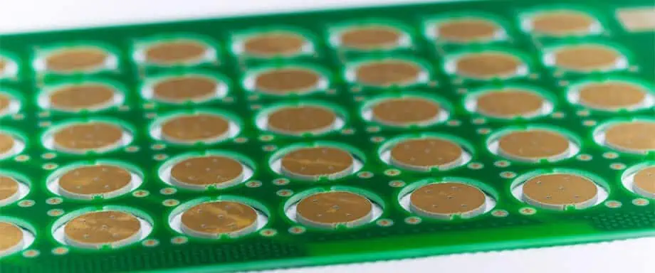
Several materials are used in the production of printed circuit boards. PCB laminates are frequently made using fiberglass. Modern PCBs have benefited from this material. For the majority of applications, laminate composites that are fiberglass reinforced offer tremendous advantages.

Fiberglass has become more prevalent in PCBs as technology has developed. New fiberglass is available with the best possible resin systems and greater characteristics. The electronic industry’s requirements for performance and cost have been met by this material.

What Does a Fiberglass Circuit Board Mean?

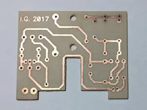
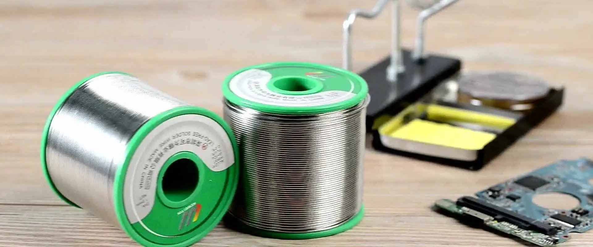
Regularly utilized for rigid pcbs is fiberglass. Fiberglass and composite materials make up the fiberglass Circuit board. This PCB also has outstanding mechanical and dielectric qualities. It also has heat resistance and moisture resistance. Additionally, fiberglass serves as a very reliable insulator.

This is a typical substrate used in PCB production. Fiberglass also strengthens its polymer matrix for producing a composite. Glass fiber can be described as reinforced plastic that is used to make fiberglass, a material that has been strengthened with fiber. This is also known as glass reinforced plastics.

Additionally, fiberglass is a lightweight and less brittle material. However, this substance may be molded into a variety of intricate shapes. It is utilized frequently in PCB production because of this, among other things. Excellent characteristics of fiberglass Circuit boards make them resistant to corrosion. Additionally, this board doesn’t carry electricity. As a result, it eliminates the possibility of any galvanic corrosion and acts like an insulator.

Glass Fiberglass Circuit Board Construction

Shengyi S1000h PCB

Placing the fiberglass fabrics on the warp beam is the first step in the manufacture of fiberglass Circuit boards.

Over the master beam, this beam has strands of coiled yarn. Its warp direction is made up of these yarns. The producer then passes some lubricants through these warp yarns. As a result, it aids in avoiding any harm during weaving.

Additionally, this warp beam is positioned on the loom’s back to begin the weaving operation. These fill yarns are inserted by the manufacturer simultaneously with the time that the yarns are moving from the loom’s rear to the loom’s front. These Draper looms have been initially accessible. The wooden shuttle will be used to go from one side of this loom to the other in this instance. These fill yarns can be inserted more easily this way.

The more recent looms run on an air or water jet. These fill yarns are being moved throughout the loom by the jet. Additionally, in contemporary looms, the warp beam might have thousands of meters of different warp strands. The producer weaves the glasses and then rinses them with water. Additionally, this aids in removing extra size from these yarns.

The manufacturer then bakes these warp yarns for a considerable amount of time. This fabric is next given a finishing treatment. Additionally, the maker strengthens the board by adding multiple resins after the weaving of the fiberglass.

What are the Characteristics of the Fiberglass Circuit board?

FULL PCB MANUFACTURING Quote

Due to its special qualities, fiberglass Circuit boards are frequently employed in certain applications.

Resistance to moisture

Fiberglass is naturally capable of withstanding moisture. Additionally, fiberglass Circuit board is not moisture absorbent. It is therefore perfect for usage in situations that are subject to dampness. This PCB is resilient to all circumstances it finds itself.

Dimensional stability

In reaction to a specific temperature, the size of fiberglass PCBs stays the same. The PCB has a very high level of dimensional stability. It is hence appropriate for applications of high power. Additionally, the board’s linear expansion coefficient is low. As a result, it is not susceptible to any changes in temperature and hygrometry.

Chemical resistance

Another fantastic quality of fiberglass boards is its chemical resistance. The majority of chemicals have little impact on fiberglass circuit boards. Strong alkaline compounds, however, may harm fiberglass.

Resistance to fire

Fiberglass neither supports combustion nor burns. Additionally, this inorganic substance is naturally inflammable. As a result, it doesn’t emit smoke when heated. Additionally, at 540 degrees Celsius, fiberglass still has roughly 25% of all its strength.

Electrical attributes

The utilization of fiberglass boards for electrical insulation is excellent. These boards also have great strength and a low Dk (dielectric constant). As a result, they are perfect for different high-end applications and uses.

Thermal Conductivity

For high-power applications, fiberglass circuit boards are the best choice due to their low CTE as well as thermal conductivity. Additionally, because of its limited thermal conductivity, this could quickly release heat.

Great Strength

Boards made of fiberglass offer a high strength to weight ratio. As a result, they are regarded as a fantastic choice for applications that need high strength.

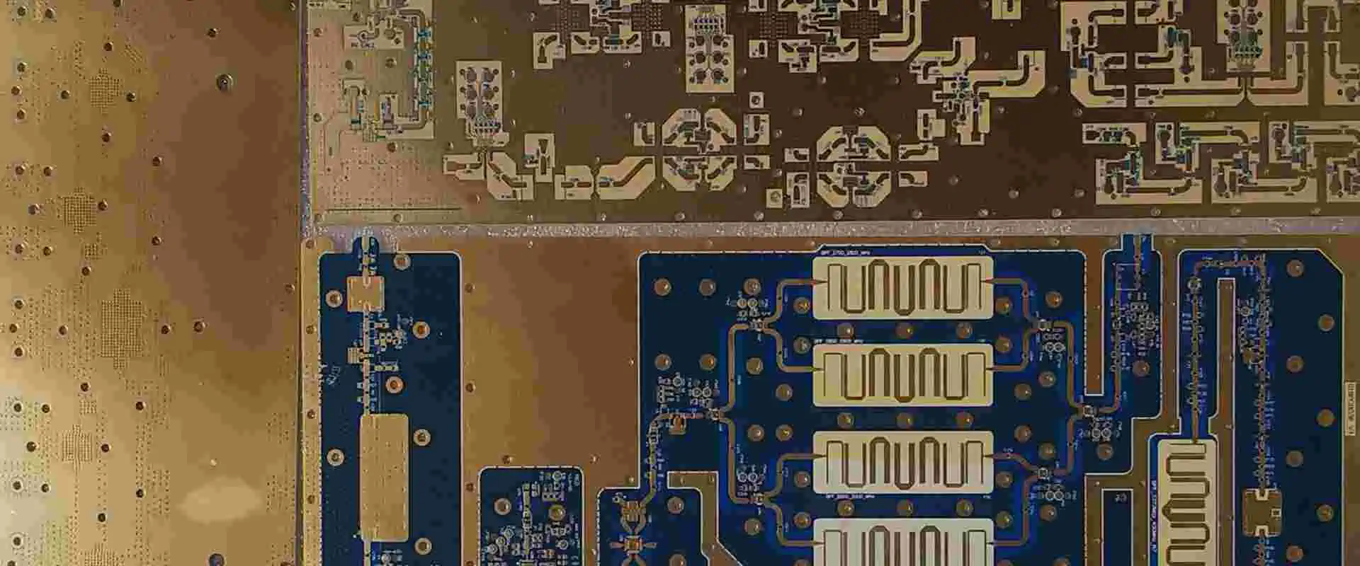
Fiberglass Circuit Board PCB Applications

Thermal barriers are provided by PCBs with high-temperature insulation. Fiberglass is inherently reliable and secure. As a result, it is a frequently used material in PCB construction. Furthermore, the following applications are frequent places where fiberglass boards have been used:

Defense and Aerospace

In applications related to aerospace and military, fiberglass circuit boards are frequently employed. These boards also aid in the production of aerospace device components. GRP is also widely utilized in the aircraft industry. Storage bins as well as instrument enclosures are a couple of examples of the GRP applications.

Consumer Electronics

Fiberglass PCBs are a common component of consumer electronics including computers, radios, as well as telephones. These boards also have excellent mechanical and electrical qualities.

Medical

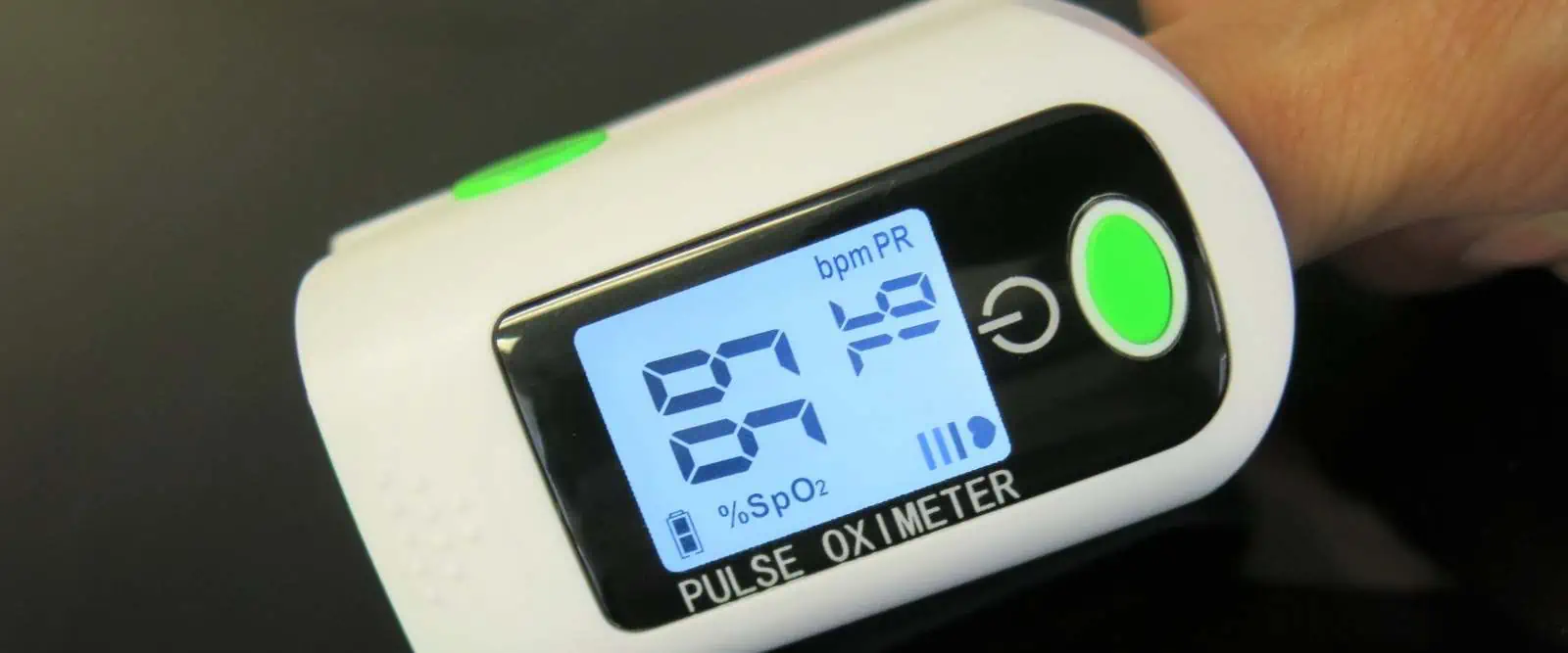
The fiberglass PCB that is frequently found in medical equipment has a low heat conductivity as well as dimensional stability. Additionally, this form of Circuit board is used in several medical devices including X-ray machines.

Automotive

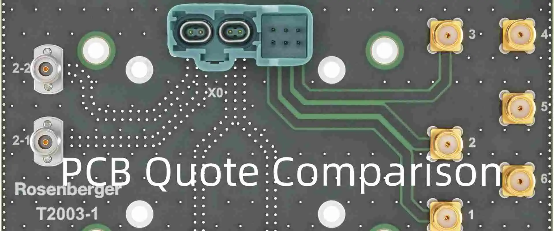
Fiberglass boards are essential to the automotive sector. The automotive sector makes substantial use of these boards. They are frequently employed in the production of automotive parts.

Conclusion

A major part in the creation of electrical devices is played by fiberglass Circuit boards. Also, these circuit boards are quite adaptable. Consequently, they are appropriate for usage in a variety of applications.

The Most Important Things to Consider During PCB Quote Comparison

pcb quote comparison

Your success as a professional OEM (original equipment manufacturer) is heavily reliant on the usability and longevity of your products. These circuit boards that you utilize are possibly the most crucial component throughout this regard. PCBs, which act as the brain of different electronic components, are used in a broad variety of ways, including connecting different components through a network of interconnected circuits.

Choosing the best PCB manufacturer is the initial step in making sure that your Circuit board needs are properly satisfied. You should thoroughly have a PCB quote comparison because you have a wide selection of options, including board houses and full-service manufacturers. This will guarantee that you receive circuit boards of the finest quality at a reasonable cost.

Questions to Ask Yourself During PCB Quote Comparison

Instant PCB Quote

During PCB quote comparison, the best seven questions to ask yourself are as follows:

  • Which manufacturers can handle low-volume orders?
  • Which credentials do these manufacturers possess?
  • How long is its lead time?
  • Is the quality appropriate for your needs?
  • How much does it cost?
  • Do you require complex Circuit boards?
  • Are the producers flexible and quick to respond?

Which manufacturers can handle low-volume orders?

Circuit board manufacturers occasionally serve a particular market or demand. You can also need an exceptionally large or lower number of Circuit boards, depending on your project.

Manufacturers prefer it ideally if customers place large orders. A big order for you can, however, be a tiny one for another business. This is a reason why it’s important to pay attention to the least or minimum order quantity for each PCB manufacturing quote.

Find a business that can meet the minimum order requirements. You should keep in mind, though, that this order volume might have a big impact on the price of PCB manufacturing. Thus, pay close attention to the PCB manufacturing quote’s rates that are supplied for the minimum order quantities. To keep expenses down, you might discover that you need to acquire more than you actually need.

What Credentials Do These Manufacturers Possess?

Users of defective electrical equipment may be in danger. An electrical fault that results in a fire and possibly an explosion is among the biggest threats. As a result, before any equipment is made available on the market, then there’s a need to first be approved for safe use, and strict procedures are in place to make sure of this.

There are a number of certifications which manufacturers should possess depending on the sectors they service to show their dedication to manufacturing high-quality PCBs in accordance with industry requirements. Since consumers may contact with the products, it is your duty to make sure that your manufacturer gets licensed and compliant.

How long is its lead time?

When you have experience in this field, you are well aware of how strict deadlines are. Comparing PCB quotes is more about getting the greatest overall deal rather than just the lowest pricing. This lead time can be described as a crucial element. Your Circuit board manufacturer should be able to provide prompt and accurate deliveries.

Learn about the delivery schedules, turnaround times, and the distance between their facilities and yours. If the orders aren’t delivered on time, it won’t matter if the seller provides the most affordable prices.

Is the Quality Appropriate for your needs?

FULL PCB MANUFACTURING Quote

Quality is the one thing which cannot be compromised whenever we talk of class 3 as well as class 2 circuit boards. This is also one aspect that differs significantly between manufacturers. Your equipment will not satisfy your clients’ needs if the Circuit boards that you order are subpar. In the end, this will result in a poor reputation in the sector.

Although a manufacturer can hardly ever have a zero defect rate, you would like to ensure it’s the lowest possible. Ask the company about quality assurance procedures they work with.

The usefulness of the quality assurance as well as quality control in design as well as prototyping helps minimize errors. This is crucial since even the smallest mistakes can be expensive to correct.

Every level of growth should include quality control procedures, which should be backed up by exemplary client care and outbound inspection.

How Much Does It Cost?

Certainly, the price is what you’ll notice first on your PCB prototype quote. The cost is important, too, along with quality. It affects your entire product pricing as well as your profitability and competition. Three key elements frequently have an impact on PCB prices: volume quality, and design. The secret involves striking a balance in-between product quality and fair price.

Low-quality Circuit boards could be less expensive up front, but they’ll cost more in the long run. But, you also should avoid purchasing PCBs at exorbitant costs. High costs will make the products relatively pricey even though the quality seems unquestionable, which will lower sales.

Do you require complex Circuit Boards?

The quantity of labor and technical knowledge required to produce circuit boards rises with their complexity. Because of this, its production quality obviously varies through different manufacturers. Complex Circuit board projects cannot be handled by all manufacturers.

Establish your needs before you start looking for a Circuit board manufacturer. Moreover, consider how sophisticated the Circuit boards you want are. Your search should be guided by this.

Some Circuit board manufacturers now focus only on a single industry. This type of manufacturer can be perfect for you because they already possess expertise, credentials, and knowledge in this field.

Are the producers flexible and quick to respond?

quote for prototype pcb assembly

Giving the manufacturer the necessary information is crucial if you want your Circuit boards to match your needs. As a result, your order needs to be accompanied all necessary paperwork. They consist of:

  • Bare board print
  • Assembly print
  • Bill of materials
  • List of authorized vendors

Rarely, you might need to change your order. Although your manufacturer may have major difficulties as a result of this, they ought to be very flexible to take such adjustments into account. Most importantly, in order to prevent delays, they ought to be sufficiently responsive and carry out such adjustments swiftly and effectively.

Conclusion

Choosing the best PCB manufacturer is the initial step in making sure that your Circuit board needs are properly satisfied. You should thoroughly have a PCB quote comparison because you have a wide selection of options, including board houses and full-service manufacturers.

What is SIM800C GSM MODULE in Electronics?

Sim800C

GSM or SIM modules are widely utilized in Internet of Things (IoT) projects due to their capability to transmit & receive data with limited dependencies compared to Wi-Fi & Zigbee. GSM modules offer reliable and long-range communication, requiring only a single SIM card with an active plan. Despite the limitation of not being able to transfer large amounts of sensor-generated data, GSM modules are ideal for different procedures that require transmitting modest amounts of information.

In our tutorial, we will demonstrate how to connect a GSM module to an STM32F103C8 GSM Module microcontroller to send & receive messages from a specified cellular phone number. A 16×2 LCD screen will be utilized to display both incoming and outgoing messages, and two buttons will be incorporated to initiate the sending & receiving of messages upon pressing.

Many projects use GSM technology and connect it to different types of controllers. You may explore these projects by visiting a website and seeing how they were made. You can even try making your own by looking at tutorials that show how to use different types of GSM modules, like SIM900, SIM900A & SIM800.

SIM800C GSM Module

The SIM800C Module is a popular GSM unit with a serial modem and operates within a voltage range of 3.4V to 4.4V. It is designed for use in projects where transfer of data is needed and can connect to four different frequencies. The SIM800C can make and receive calls and send and receive text messages with low energy consumption. It is controlled using special AT commands and can only support one card of SIM. The module has special pins for communication (TX and RX) and can connect to different microcontrollers using the RS232 serial protocol.

Powering SIM800C Module

A 12V Direct Voltage or Direct Current power adapter powers the SIM800C module GSM.

Insert SIM

You insert a card of SIM into the back side of the SIM800C module GSM. Remember that this module does not work with 4G SIM cards, so only use a regular card SIM.

Interfacing SIM800C Module with STM32F103C8 Module

To connect the SIM800C to the STM32F103C8 microcontroller, we will use the UART port, a unique communication tool built into the STM32F103C8. The pins of UART on the STM32F103C8 are labeled as A9 & A10, as shown in the image. The STM32F103C8 Module has 3 UART interfaces that can be used to connect to three different external devices that use serial communication.

Programming STM32F103C8 Module Microcontroller for interfacing

FULL PCB MANUFACTURING Quote

The ARDUINO software can be useful to write code for the STM32F103C8 microcontroller. In our tutorial, you do not need an exceptional programmer like FTDI/ST-LINK. To upload the code, connect the micro USB port on the STM32 to your computer using a USB cable, and then you can start writing the code in ARDUINO IDE. Before writing the code, you need to add the required libraries for the peripherals used in this tutorial and define the pin configuration for the LCD.

Next, initialize the LCD (Liquid Crystal Display)by selecting LCD to begin(16,2), where the parameters specify the type of LCD, which is a 16×2 block. To check if the LCD is properly interfaced and producing output, print a debug message.

Set the direction for the push button data as input mode and define the corresponding PIN.

Pick a speed for sending information through a serial connection.

The code contains two functions, one for sending messages and the other for receiving messages.

ยท Send Message

This function helps you send text messages to a phone number. First, a special command called AT is propel to the GSM module to tell it you want to send a message and what number to send it to. 

Then, another command called AT+CMGS is sent to the module through a port called serial1, and this command tells the module to actually send the message to the specified number.

To send messages, the special command “AT” is sent every second. After sending the message, another command called “CTRL+Z” must be sent to the GSM module through a port called Serial1. This will cause a unique code to be sent to the GSM module.

Once the message is sent successfully, a message saying “SMS sent” will appear on a screen called a 16X2 LCD.

ยท Receive Message

This function utilizes the AT command to receive and display live messages on the LCD screen.

When you get a text message, it has some information like the time and date. The message is found after the sixth quotation mark (“). The rest of the text is the message you received.

How to Send & Receive Text Messages using STM32 Module? 

esp32 sim800c

1. For sending a text message, push the button on left side. The message will be drive to the phone number specified in the system.

2. For getting a text message, push the button on right side. The message will appear on the screen. That’s how you use a GSM module and an STM32F103C8 microcontroller together. If you have any questions or ideas, please let us know by leaving a comment.

Features of SIM800C GSM MODULE 

This tiny module is only 1 inch square, but it has many features packed into its small size. Here are some of them:

  • Works with four frequency bands: GSM850, EGSM900, DCS1800, and PCS1900.
  • Connect to any global 2G GSM network using any 2G SIM card
  • Create and answer voice calls utilizing an external 8ฮฉ speaker and an electret microphone.
  • Send & receive SMS 
  • Send & receive GPRS information 
  • Scan & receive FM broadcasts

What are the Parameters and Processes Involved in Manufacturing an Etched Circuit Board?

Etching Solution for PCB

One crucial step in the manufacture of PCBs is PCB etching. The intended circuit layout must be revealed by eliminating copper out from the PCB’s surface. All copper on the PCB is removed during the etching process, with the exception of the circuitry which is tin-plated for protection. Its copper is then cleaned once the tin has been extracted.

Though it seems simple, the etched circuit board process is highly intricate, and accuracy is crucial. Also, a variety of Circuit board etching techniques can be used, and each one has advantages and disadvantages of its own. We’ve created this tutorial to give you more information on the circuit board etching procedure.

What Does Etched Circuit Board Mean?

A circuit board’s undesirable copper is eliminated through the process of Circuit board etching. Only the necessary circuit is left on the PCB after all of the extra copper has already been taken off. The circuit board’s layout is prepared prior to the start of the etching procedure. Photolithography is the method used to put the desired board layout onto the PCB. This serves as the pattern for selecting the copper pieces that must be taken off the board.

Tin plating serves as an etch resist on the PCB’s outer layer. This etch resist is the photoresist in the internal layer, though. In general, there exists two methods for etching the outer and inner layers of a PCB. These include wet etching and dry etching.

The Dry Etching Process

PCB-etching-materials

In order to start chemical interactions between the laminate’s surface atoms and base, dry etching typically requires plasma. The undesirable copper dissolves as a result. Although plasma has been frequently used during dry etching, lasers can also be used.

Plasma etching

Since 1960s, this has existed. It didn’t become well-known, though, until about the 1970s. This method was developed to assist manufacturers dispose of liquid waste more sparingly while still achieving selectivities which were challenging to accomplish using wet chemistry.

During plasma etching, the PCB is exposed to high-speed glow discharge stream from a proper gas mixture. Hence, plasma etching can be described as a dry, clean procedure that doesn’t need any chemicals.

Moreover, plasma etching has the ability to do precise and controlled small scale etching. It’s also quite popular since it makes it less likely that solvents will penetrate into vias or that they will get contaminated.

Plasma etching, despite its benefits, is exceedingly expensive. Due to this, it will probably be significantly more costly than the wet etching process unless you consistently etch large quantities of material.

Laser etching

Utilization of precision, computer-controlled hardware is made possible by laser etching. A powerful laser is used to create trace lines upon that PCB’s substrate during the procedure. These undesirable copper wires either disappear completely or flake off the printed circuit board.

As one of its key advantages, laser etching reduces the amount of steps involved in the whole process. Also, it does away with the usage of any harmful chemicals, acids, or inks.

Large boards can be challenging to etch them evenly, and residues and etchant might be challenging to remove if they wouldn’t completely evaporate. Also, the procedure for laser etching is quite expensive, just like plasma etching.

Wet etching

Unwanted copper is removed during the process of wet etching using a solution which undergoes chemical reactions. Acidic chemicals or alkaline chemicals could be employed for the process, depending upon that etches substance.

Acidic etching

Here, the rigid PCB’s inner layers are typically removed using the acidic approach. Either ferric chloride or cupric chloride is employed in this method. The more popular of both, cupric chloride, precisely removes tiny features while offering a steady etch rate as well as continual regeneration.

As the acid will not really react with photoresist or harm the necessary component, the acidic technique is typically employed for the innermost layer. Moreover, the undercuts, which is described as the etched material’s lateral erosion beneath the shield of tin/leadโ€”are minimized. Yet, compared to alkaline etching, the acidic etching may be a time-consuming operation. Due to this, ย it isn’t usually appropriate for significant numbers of Circuit boards.

Alkaline etching

Circuit board’s outer layers are frequently removed using the alkaline technique. Also, this is how we operate. A PCB can be quickly and affordably etched using alkaline etching. The procedure must be constantly monitored, though. This is due to the fact that prolonged contact with the solvent may cause harm to the board.

Alkaline etching can often be done in a high-pressure, conveyorized spray chamber that makes the entire process as fast, efficient, and precise as possible. The Circuit board is subjected to a fresh etchant inside the chamber.

The breakpoint refers to the stage of the etching when all of the undesirable copper has been removed. Typically, this is accomplished at the spray chamber’s halfway.

Parameters that Impact the Etched Circuit Board Process

FULL PCB MANUFACTURING Quote

The etch rate you acquire is influenced by both the etched time and the etching solution’s composition. By regulating specific parameters, the process of etching can be made to be of high quality. Let’s think about them

Temperature

Remember that most etching machines would be made of plastic components because such metallic parts have become reactive to etchants when adjusting the solution’s temperature. The temperature must not be extremely high if the plastic parts on the etching machine are plastic. The optimal temperature range in this case is between 50 and 55 degrees Celsius, or 122 to 131 degrees Fahrenheit.

Unique Gravity

The etchant’s concentration was associated with specific gravity. Typically, a larger number corresponds to a greater etch rate. For the alkaline etching, the parameter becomes particularly significant when focusing on the solution’s pH. When the solution’s pH varies from 7.9 to 8.1, alkaline etching could be done successfully.

pH

When the solutionโ€™s pH is below 8.0, there may have been insufficient ammonia or excessive ventilation that caused the pH to decrease. Remember that when a pH is greater than 8.8, the etching rate could be low. Whereas if the etchant has absorbed water or contains an excessive amount of copper, this problem may arise. Any rise in pH levels could lead to inaccurate readings being acquired for the acidic etching.

Since the harsh plating solutions might harm electrodes not suited for the plating applications, pH monitoring in the plating solutions could be challenging. Many plating applications call for the Sensorex pH Electrode, which is built to tolerate harsh circumstances.

Concentration of the Chemical Additive

The etching rate can be efficiently increased by using chemical additives. Hydrochloric acid is the most widely utilized addition because it can improve an etchant’s capacity to cling to dissolved metals. Chemical additives have been required when a manufacturing or industrial facility needs constant etching. Even when additions complicate etchants, its etching rate will always increase.

Possibility for Oxidation-Reduction

The oxidation and reduction potential that describes how active this etchant is, is the final and fifth parameter. The ORP immediately reveals the relationship between cupric and cuprous ions as well as how these ferric ions can relate to the ferrous ions.

The etchant’s initial cupric or ferric state will shift to a ferrous or cuprous condition when the copper has been etched.

You could be sure that the etching rate is high if you measure the ORP to be high. The low ORP levels indicate a less effective etchant. The temperature of the etchant and the content of the free acid can both be used to calculate a solution’s ORP value. It is feasible to convert these cuprous ions back to the cupric form by adding an oxidizer as well as a free acid into the etchant.

What Phase of the production process is the Etched Circuit Board At?

Strip film etching line

Near the conclusion of the process of circuit board manufacturing is the circuit board etching procedure. Although the actual PCB fabrication process is challenging, we have simplified it.

The etching procedure can start after the Circuit has been tin-plated, which helps safeguard the board. Here, the board is run through a conveyorized PCB etching equipment, that sprays it using a amonicon solution, to etch the area surrounding the traces. This eliminates any exposed copper on the circuit board’s surface that is not covered by tin plating, retaining just a covered tracking.

The board is dried as well as thoroughly examined after the etched circuit board procedure. It is subsequently run through the tin-stripping machine. The tin covering the residual copper traces is removed by this machine using nitric acid.

The etched circuit board process is finished at this point, and the circuit board can move on to the production phase.

Conclusion

Etched circuit board has to do with the elimination of any undesirable copper present in any circuit board through the process of Circuit board etching. Only the necessary circuit is left on the PCB after all of the extra copper has already been taken off. The circuit board’s layout is prepared prior to the start of the etching procedure.

The Significance of the Finger Oxygen Sensor

Finger oxygen sensor

Your doctor might advise using the pulse oximeter if you suffer from a heart or lung issue or experience breathing difficulties as a symptom. An electronic instrument called the pulse oximeter, often known as the finger oxygen sensor, detects oxygen saturation transported by the red blood cells.

You can put pulse oximeters on your forehead, fingers, foot, nose, toes, or ears. The gadget can then be recycled or thrown away. Ask your doctor before throwing away a pulse oximeter if you’re using it at home because they can be pricey and are reusable. The FDA issued a warning about the restrictions placed on pulse oximeters around February 2021.

The pulse oximeter could provide erroneous or irregular readings if you possess poor circulation, thick skin, dark skin coloration, presently use tobacco, the skin temperature seems chilly, you are putting on a dark fingernail lacquer, artificial, long nails, and if the fingers are unclean. This explains why it is improper to utilize the pulse oximeter’s readings alone to assess your health. This is crucial to inform your healthcare practitioner of any inconsistent or abnormal readings.

How Do Finger Oxygen Sensors Work?

oxygen monitor for covid

The instrument known as the pulse oximeter often is worn on the fingertip. This calculates its pulse rate as well as blood’s oxygen saturation using laser beams. The oxygen conveyed in blood is revealed by oxygen saturation.

Without collecting blood sample, a pulse oximeter could determine the quantity of oxygen present in blood. A pulse oximeter typically displays two to three numbers. This oxygen saturation level, which is the most crucial figure, is typically abbreviated as SpO2 and displayed as percentage. PR is t he abbreviation for pulse rate, which is akin to the heart rate, and there may occasionally be a third digit for signal strength.

Most healthy people have oxygen saturation levels between 95% to 100%, although patients with lung issues can have lower numbers. Higher altitude residents typically have slightly lower levels of oxygen saturation. Pulse oximeter measures the amount of the oxygen saturation within your blood quickly and painlessly without drawing blood or using needles.

The red blood cells’ oxygen saturation is represented by the specified volume that is displayed on screen. This figure helps your medical professionals and nurses plan your care. You might be able to tell if you really need additional oxygen by looking at the level of oxygen.

The saturation measurement, which should be above 90 to 92 percent, differs from the pO2 value, which is determined by drawing blood from the artery and should be above 60 to 65 percent. Your doctor may explain how your value relates to your specific scenario.

The Operation of the Finger Oxygen Sensor

Oxygen saturation is measured by clip-on devices called pulse oximeters. The gadget can be fastened to a wrist, finger, foot, as well as other locations where blood flow can be detected.

The way pulse oximeters operate is by shining the light via a section of skin that is quite transparent. On the opposite side of a skin, a detector receives the light as it passes through.

A side of this clip, for instance, shines light whenever the pulse oximeter gets attached to the finger, while the other side detects it.

Also, the quantity of light that the blood can absorb determines its oxygen saturation. In order to determine the precise amount, a finger oxygen sensor estimates its oxygen saturation rather than measuring it directly.

What Dangers Do Finger Oxygen Sensors Pose?

FULL PCB MANUFACTURING Quote

Devices for measuring pulse oximetry are noninvasive therefore pose no major dangers. Minor skin sensitivity and redness are small irritations that some people feel.

Pulse oximeters may prevent blood vessels in the area from receiving oxygen if they are fitted snugly and worn for a long time. Anyone who feels tingling, numbness, or abnormalities in their skin tone should call their doctor right once.

A false measurement is the primary danger of the pulse oximetry or finger oxygen sensor. The fit of the pulse oximeters is crucial for accuracy, and even little adjustments to their location can result in misreading. Rolling over while sleeping could loosen the gadget and result in false alerts.

Other variables, such a sleeping posture change or a short breath-holding, can also cause oxygen saturation to temporarily drop. Even if the dip is brief and unharmful, the finger oxygen sensor will inform the user.

This can result in unnecessarily worrying patients who have health concern and whose doctors haven’t yet explained the function of the pulse oximeter to them. In contrast, some persons may feel deceived into feeling secure by pulse oximeters. They cannot replace other monitoring measures and do not offer warnings for all potential oxygen problems.

Individuals who use pulse oximeters must talk to their doctor about the hazards and keep track of their readings through time. Readings that fluctuate, especially during environmental changes, can occasionally indicate a health issue. Before purchasing a device, those interested in utilizing pulse oximeters (consumer-grade) should review their goals with the doctor.

What are the Advantages of the Pulse Oximeter?

Pulse oximeters can be used by those with complications related to oxygen saturation. A doctor may advise using the pulse oximeter to check the nighttime level of oxygen saturation in patients with severe snoring or sleep apnea.

Pulse oximetry is a tool used by medical professionals to assess the physical activity’s safety especially for those with respiratory or cardiovascular conditions. They might advise the individual to wear the pulse oximeter when engaging in physical activity.

Particularly in infants, the pulse oximeter can be utilized to indicate dangerously low levels of oxygen. When a person is under anesthesia, pulse oximeters serve to measure the levels of oxygen saturation.

Pulse oximeters can be used to detect signs of drug use in patients who may have breathing problems as well as issues relating to the levels of oxygen saturation.

To determine whether additional oxygen is required, the pulse oximeter can be utilized. Oxygen saturation can be continuously monitored using the pulse oximeter. Pulse oximeters nowadays are conveniently available online. Hence there are no risks associated with their use for people.

There are several companies that offer pulse oximeters for parents of newborn and infants. Parents that are concerned regarding the infant death syndromes as well as sleeping mishaps can relax thanks to these gadgets. Yet, there is no evidence to back up the assertion that the pulse oximetry may stop accidents or SIDS.

Downsides of Pulse Oximetry

fingerprint sensor schematic

The accuracy of the reading of the pulse oximeter can be affected by a number of things. As follows:

  • Whenever the pulse changes
  • There may not be a pulse oximeter alert whenever there is poisoning from carbon monoxide.
  • As a result of bilirubin levels
  • As a result of blood pressure lipids
  • When interference from outside color or light, such as nail polish, occurs
  • Those with chilly hands or weak circulation
  • Individuals who use pulse oximeters to check their oxygen saturation shouldn’t rely on the device in place of their own judgment.

Individuals should seek medical attention right away if they develop breathing difficulties, lightheadedness, difficulty breathing, or any other indicators of potential oxygen deficiency.

Reading the Pulse Oximeter Correctly

The device would show your heart rate and the level of saturation of your oxygen after you take your reading. Your level of oxygen is indicated by the number underneath or adjacent to the “SpO2.” Your pulse is the number that appears beneath or right next to the heart symbol or the heart rate.

Your healthcare practitioner should offer you guidance on what you should do if your pulse oximeter readings were lower or higher than expected if they have recommended that you use one at home. If you’re unsure of what’s best for you because this varies from one individual to the other, it’s always better to inquire.

The following general principles should be followed when analyzing the reading of the finger oxygen sensor:

  • Measure the amount of oxygen in your blood. The majority of humans require oxygen saturation levels of at least 89% to maintain healthy cells. Does your reading fall within or exceed this range?
  • Compare the results to your starting points. It’s crucial to evaluate your reading in relation to your starting points. For instance, you shouldn’t delay until the levels are lower than 89%, when the baseline level of oxygen saturation is 98%, before seeking medical care.
  • Take accuracy rate into account. The typical accuracy rate for prescription oximeters is 4% below or above a reading. As a result, a 92% oxygen level could potentially be 88% or 96% higher. Moreover, measurements from pulse oximeters are frequently most accurate when they are over 90%.
  • Pay attention to your body. When deciding whether or not to seek medical attention, you shouldn’t depend on the reading of the pulse oximeter alone.

Conclusion

One important at-home devices for pulse oximetry in use are finger oxygen sensors. This technique is the most efficient at allowing a quick lifestyle, as it is made to make obtaining the levels of oxygen saturation as painless and quick as possible.

Applications of a Printable PCB

Rogers RO4835T PCB

If you dismantle an electronic device, you will find a small green board. This board is what we refer to as a printed circuit board. It functions as the life of that electronic device. An electronic or electrical device canโ€™t function without this board.

The green board you see in your electronic device has markings that look like a maze. A printed circuit board allows connections between components. All PCB boards are printable as they allow you to print a specific design on them.

What is a PCB?

A printed circuit board offers mechanical support and connection to electronic components via pads and conductive pads. Furthermore, a PCB features pre-designed copper tracks. These tracks minimize wiring and as such decreases the errors that arise as a result of loose connections.

PCB lays the foundation for the assembly of components. When manufacturing electronic devices, components are usually placed on the bare circuit board. A PCB is a bare board that features pads and conductive tracks. The placement of electronic components like resistors, capacitors, and more makes a PCB a fully assembled board.

What is a Printable PCB?

Rogers-RO4534-pcb

The manufacturing of a printed circuit board goes through several steps. Manufacturers ensure they carefully carry out these steps to achieve a functional board. Printing the design is one of the crucial steps involved in PCB manufacturing. A printable board is a board that has a film which reveals its layers and details.

A plotted printer is used in printing the design of the board. A printable PCB has two ink colors on the layer of the board. The white ink reveals the non-conductive areas while the blank ink reveals the circuits and conductive copper traces. Some manufacturers fabricate printable PCB using specialized PCB 3D printers. These printers are much faster than plotted printers.

Steps Involved in Manufacturing a Printed Circuit Board

Design

Before the manufacturing process commences, you need a design. The design is a blueprint in which the manufacturer begins the process. A computer software application is usually integrated for this step.

Print the design

Creating a design doesnโ€™t just end there. In this step, you will be printing the PCB design with the help of a plotted printer. The PCB will have two different colors of ink.  A clear ink and a black ink. The black ink reveals the circuits and conductive copper traces.

Creating the substrate

In this step, the manufacturer pre-bonds the copper to both sides of the layer. The substrate holds the components. It is the base of the material.

Inner layer printing

Here, the design is printed to the body of the structure, which is usually called the laminate. The photo-sensitive film will harden when you expose it to ultraviolet light. With this, the blueprints and the specific print of the circuit board will be aligned. Also, to aid the alignment process, the manufacturer drills holes in the PCB.

Unwanted copper removal

The PCB manufacturer will need to get rid of unwanted copper from the circuit board. Here, the board is dipped in a chemical solution that gets rid of the unwanted copper.

Inspection

FULL PCB MANUFACTURING Quote

There is a need to inspect the layers to ensure alignment. The drilled holes help in aligning the outer and inner layers. Inspection is necessary to ensure the boards are not defective.

Solder mask application

The panels of the PCB need to be properly cleaned before applying solder mask. The manufacturer then applies the epoxy with the solder mask. An ultraviolet light helps to remove unwanted solder mask.

Silkscreening

This is an important step in PCB manufacturing. Silkscreen prints crucial details on the board. After applying silkscreen, the PCB goes through a curing process and one more coating.

Surface finish

This step involves the application of coating on the board. Surface finishes are available in different types. Coating the board with a surface finish helps in preventing the copper in the printed circuit board from oxidizing.

Testing

An electrical test is usually performed on the circuit board. This helps in confirming the functions of the circuit board.

Applications of Printed Circuit Boards

Copper Coin PCB

Printed circuit boards are applicable across several industries ranging from the medical to military and consumer electronics.

Consumer electronics

Consumer electronics are electronic appliances we use everyday. These include televisions, smartphones, and computers. PCBs play a crucial role in the development of these electronics. Some consumer electronics require the use of advanced PCBs while some require simple PCBs. Circuit boards integrated for consumer electronics should be low-cost.

Automotive components

Automotive parts and components features PCBs. In the past, circuit boards were widely integrated for vehicle parts such as headlight switches and windshield wipers. However, things have changed as PCBs are integrated in advanced features. PCBs are now being used in control systems, sensors, and navigations systems of vehicles. The majority of the systems that regulate the function of a vehicle depend on electronics powered by circuit boards.

Medical devices

There is a growing use of printable PCB in the medical industry. As technology advances, more and more medical devices are being innovated. All these innovations were made possible due to printable PCB. This circuit board is available in medical devices like infusion pumps, medical imaging systems, internal devices, and monitors.  PCB manufacturers need to pay attention to the PCBs used in the production of medical devices. These boards must meet some strict standards to ensure safety.

Aerospace components

Aerospace devices are usually exposed to harsh weather conditions. Therefore, high-end PCBs are widely integrated for the manufacturing of these devices. Printable PCBs are a core component in power supplies, communication equipment, and monitoring equipment used in the aerospace industry. These boards are necessary for the development of aerospace components.

Conclusion

PCB lays the foundation for the assembly of components. When manufacturing electronic devices, components are usually placed on the bare circuit board. A PCB is a bare board that features pads and conductive tracks. The placement of electronic components like resistors, capacitors, and more makes a PCB a fully assembled board. Printed circuit boards are applicable across several industries ranging from the medical to military and consumer electronics.

Unnoticed Uses and Making of 100K Resistor

100K-Resistor

You may have heard of resistance. It disrupts the electrical current. As the word suggests, the main purpose of the resistor is to reduce the flow of current, divide voltage and adjust the signal level. The electric resistance is measured in Ohms. When it comes to resisting current, we have several types of resistors, from wire wound resistors to thermistors. Letโ€™s dig deeper to know more about the 100k resistor and what are its uses, and how it is different from the rest of the resistors.

What is a 100K Resistor?

As the name suggests, the 100K resistor constitutes 100,000 ohms of resistance. When compared to the other resistors, a 100K resistor is the uppermost limit of the resistors that companies around the world make.

 What Is The Color Code of the 100k Resistor?

10k ohm

Color code is the identification of any resistor. A layman may consider it some ordinary line on a resistor. A circuit designer or electrical engineer knows well the purpose of these lines. Color codes have some values and help to calculate the resistance of the resistor.

The color code for a 100k ohm resistor is Brown, Black, Yellow, and Gold. Let me explain to you the first band is brown, and the second band is yellow. Both show digit values one and zero, respectively.  The gold band on the resistor represents the tolerance value. It means that the tolerance value may go up and down to five percent.

Uses of 100K Resistors

There are a number of uses for 100K resistors, such as:

1. Voltage Divider and time Circuits

Firstly, one common use for 100K resistors is in voltage divider circuits.  They divide the voltage properly. Similarly, time circuits also have 100k resistors. One popular example of a timer circuit is the 555 timer circuit. 100k resistor helps to delay the current flow in some circuits. It is the need for the circuit in a particular device. That’s why 100k resistors are most popular as voltage dividers and time delay circuits.

  • Biasing Transistors

Another common use for 100K resistors is in biasing transistors. Biasing refers to the process of setting the voltage levels at the transistor’s input and output terminals so that it operates in the desired way. 100K resistors are helpful in biasing circuits to help set these voltage levels.

3. Current Limiting

Additionally, 100K resistors serve a lot in limiting current. As a result, 100K resistors frequently serve as current-limiting resistors for LEDs to prevent them from burning out due to excessive current.

4. LED Current Limiting

The engineers use 100K resistors to limit the current flowing through LEDs. In order to prevent LED burnout due to excessive current flow, a current-limiting resistor is required. Sometimes delicate parts burn due to the heat of electric current.

5. Oscillators

100K resistors are in practice in oscillator circuits. 100k resistors work best in combination with capacitors and other components. So, Oscillators help generate a periodic waveform,

  • Voltage Regulators

ย A voltage regulator helps to regulate the voltage of a power supply or battery. 100K resistors in voltage regulator circuits help set the output voltage of the regulator. 100K resistors serve the purpose best in voltage regulators.

Making a 100K resistor requires some knowledge of electrical circuits and some basic materials. However, it’s important to note that making your own resistors is not recommended for most applications. A layman doesn’t have proper knowledge of parts placement. ย ย That’s why commercially available resistors are typically more precise and reliable. Itโ€™s hard to do proper testing of DIY resistors. However, letโ€™s have a look at the making of the resistor.

How to Make a 100K Transistor?

FULL PCB MANUFACTURING Quote

To make a 100K resistor, you will need a length of wire with a specific resistance per unit length. The resistance per unit length of wire is typically given in Ohms per meter or Ohms per foot.

Once you have the correct length of wire, you will need to wind it into a specific shape to create the resistor. One common way to do this is to wind the wire around a ceramic or other non-conductive core, such as a pencil or small tube. The number of turns and the spacing between the turns will depend on the desired resistance and the diameter of the core.

After winding the wire into the desired shape, you will need to measure the resistance of the resistor using a multimeter or other measuring device. It’s important to note that the resistance of homemade resistors may not be as precise as commercially available resistors and may vary depending on the specific wire and winding technique used.

Making your own 100K resistor is possible but not recommended for most applications. It requires a specific length of wire with a specific resistance per unit length, as well as knowledge of basic electrical circuits and some basic materials. Commercially available resistors are typically more precise and reliable. Thatโ€™s why engineers go for these resistors.

 Why Are 100k Resistors Most Suitable As Compared To Two 50k Resistors In A Series?

You can use two 50 k resistors instead of a single 100K resistor. Sometimes this practice doesn’t provide you suitable power rating for the application. The second thing is that stray capacitance or inductance may increase due to using two 50k resistors. That’s why a 100k resistor serves best for the purpose. Another thing is that if connecting the different resistors in series can serve the purpose, then why manufacturers are making different resistors of different resistance? Manufacturers are making resistors of some specific resistances to avoid stray capacitance or inductance issues. Thatโ€™s why a single 100K resistor serves best and is necessary for several circuits. Two 50k circuits cannot full fill the purpose.

Final Note

So, thatโ€™s it with the 100K resistor. Its high resistance makes it suitable for multiple uses. It is possible to use a 100K resistor in several ways, and it contains 100,000 ohms of resistance. We tried to cover the topic from all perspectives. Feel free to share your thoughts with us.

Is IR Reflow Superior to Vapor Phase Reflow?

IR Reflow

Our company has been constantly searching for cutting-edge technology that can speed up assembly while enhancing PCB quality. The IR reflow, which has to do with the profiling of each Circuit board type and took a significant period of time, was included among the assembly line’s bottlenecks.

Vapor Phase Reflow was discovered in our quest to increase the efficiency of the surface mount assembly process, and investing in these devices and systems has successfully eliminated delays. Here, we contrast the two soldering techniques.

Soldering Using IR Reflow

A typical technique for the quick manufacturing of PCBs is IR reflow soldering. The solder paste, made of solder flux and solder, is applied to the essential parts of the circuit board during the procedure. There is a minor viscosity to the paste. Electrical components must stick to the board as a result of this.

The PCB goes through the oven while being reflow soldered. This solder paste melts as a result (reflow). Each circuit board passes through a cooling cycle after its oven stage. These electrical components are now permanently attached to the pcb board because the solder has set.

For a few reasons, reflow soldering can be frequently used in the manufacture of circuit boards. The oven technique, in particular, has a far higher soldering capability than the hand soldering. That capability permits the manufacturing of the circuit boards in a large volume very quickly.

Second, there has been number of improvements made to ir reflow soldering techniques throughout time. These developments have made it possible for reflow soldering to produce surface mount devices with soldering of the greatest quality.

HACR Procedure

IR Reflow wave

To achieve uniform soldering throughout the board when employing the IR reflow method to solder the PCB assembly, a special reflow profile must be created. HACR procedure primarily utilizes hot air, which isn’t always an appropriate method for soldering.

The HACR profile is significantly influenced by the PCB’s thermal mass as well as the components present on it. In addition, the components’ color also affects the profile since darker colors absorb heat faster and readily than lighter or reflective colors.

These elements alter the pace at which heat is transferred from hot air immediately it circulates inside the oven.

Thermocouples are used on the test circuit assembly to measure the temperature change as it passes the oven during profiling. This approach has two shortcomings. The first disadvantage is that it takes time to complete the task because a specific temperature profile is required for uniformly proper soldering. A second problem is that if a limited run is involved, the buyer might not be ready to deliver the necessary test PCB assembly.

VPR Procedure

Vapor phase oven use the vapor layer that transfers the latent heat when it condenses, in contrast to HACR, which utilizes hot air for transferring heat into the PCB as well as its components since it moves through a system present on the conveyor belt. When a particular liquid is boiled at a temperature of 235 ยฐC within the system, a vapor layer is produced, and the latent heat gotten from this vapor is transferred very effectively, causing components with differing thermal masses to reach this very same temperature simultaneously.

Early VPR oven models were not known since a lot of this vapor leaked out, making them harmful to both the user and the environment. Moreover, its IR reflow profile was fairly dependent on the temperature range and the volume of fluid inside the tank.

Only few batches of PCB assemblies could be soldered at once due to the need for manual handling when putting them inside the oven.

Current VPR ovens have a completely new design, with this enclosure recovering nearly all of the vapor medium. The manufacturers now handle PCB assemblies automatically, making it possible to precisely monitor and regulate its temperature profile.

VPR Soldering Process

FULL PCB MANUFACTURING Quote

Since all that is required to melt its solder is the introduction of sufficient heat, soldering first appears as a straightforward procedure. Whenever the system uses solder paste for soldering SMT boards, there are many more steps involved in the process.

A copper pad just on Circuit board as well as component leads must also warm up to a temperature just above the solder paste’s melting point in order for a solder joint to be considered successful. A chilly and unsuccessful joint arises from failing to accomplish this. Also, the components should not be overheated when applying heat because this could harm them. In contrast to other soldering methods, such as radiation, forced convection, or conduction via the soldering gun, this VPR process of soldering transmits heat from the condensing vapor.

The VP reflow machines operate in a very basic manner. This vapor stage fluid sits at room temp at the fluid tank’s bottom before being turned on.

The fluid is heated to boiling after being turned on at 235 ยฐC, which is the average melting temperature of the lead-free solder pastes.

The ideal temperature necessary for melting the solder paste is 235 ยฐC, hence VPR system manufacturers explicitly engineer their products to have a boiling point for a liquid in vapor phase at this temperature. The vapor produced by the boiling liquid is thick and has sufficient latent heat to be transferred to the circuit board assembly.

Vapor condenses present on the cold circuit board assembly as it enters the tank, transmitting the latent heat into the circuit board pads and components till they all reach the equivalent temperature like the vapor. The circuit board assembly cannot become too hot due to the system.

Conclusion

For IR reflow soldering, the solder paste, made of solder flux and solder, is applied to the essential parts of the circuit board during the procedure. Vapor phase type of reflow soldering is a quick and incredibly reliable technique that our company recommends for circuit board assemblies. The technique is appropriate and dependable for soldering SMT circuit boards with a variety of complicated components, including flip chips, QFTs, ceramic assemblies, and BGAs.

Lead Free Solder Vs Lead Solder: Which is Better?

lead free solder

For so many years, the leaded solder is now the material of choice for PCB manufacturing. However, in recent years, consumers worry about the environmental and health implications of these leaded products, which has increased. These factors led to the European Union’s RoHS directive, which restricted the use of hazardous materials in electronic and electrical equipment, to take effect starting July 2006.

Some nations, unlike the U.S.A, do not have legislation that makes the use of lead within consumer products unlawful. But, some companies are requesting that the electronic device they order be made with lead solder. But again, what type of solder is recommended for usage in the electrical industry? What distinguishes lead free solder from solder that contains lead?

This piece will find answers to all questions relating to this, coupled with providing additional insights regarding lead free solder and leaded solder.

What is Lead Free Solder vs Leaded Solder?

lead free SMT solder

Solder is typically used by electronic makers to attach components to Circuit boards. All solders, whether lead free solder or with lead, have the same purpose. However, different solder techniques are used with different devices as well as use situations.

Lead Soldering

Lead and tin are the two main ingredients in leaded solder. Leaded solder’s sufficient flowing capability is a benefit. Since its melting point is lower than that of lead free solder, it doesn’t heat up components as much.

Moreover, lead free solder takes on a duller appearance whenever it cools, making it harder for users to spot problems like oxidation. Lead solder also is less expensive and simpler to use compared to lead free solder.

Lead Free Solder

The elimination of lead from electronics manufacturing as well as waste recycling procedures is the primary driver behind manufacturers’ switch to the usage of lead free solder. Alternative materials for soldering centered on the tin metal have rapidly developed over the past 20 years in the field of electronic manufacturing. The components used in this alternate method have characteristics that are different from those of the tin and lead eutectic composition.

Soldiers require performance akin to that of superalloys used in jet engines because they are functional around 80% of the melting temperature. But as things get smaller, the demands for solder junctions keep going up because to the rising stress and density characteristics. Hence, the PCB design that takes into account its melting point that is high and anisotropic features is required for lead free solders.

The Differences Between the Features of Lead and Lead Free Solder

FULL PCB MANUFACTURING Quote

When lead is used in large quantities for a long period of time in consumer goods, negative consequences on the environment, as well as on human health, results. Nowadays, businesses use lead free solder to assist the social responsibility initiatives of environmental protection.

The Melting Point of Lead Free Solder Is Greater than the Lead Solder

Lead-filled solder melts at a temperature of 1830ยฐC, whereas lead free solder melts at 2170ยฐC. The consequences of lead free solder’s greater melting point are as follows:

Compared to lead soldering, which uses a lower temperature, lead free soldering quickly oxidizes its solder. Certain components, such as those with plastic packaging as well as electronic capacitors, are adversely impacted by the higher soldering temperature that lead free solder has.

Components with a low dielectric are more prone to failure because of the high component stress caused by lead-free solder’s high temperature.

Components made with lead free solder feature a number of soldering surfaces. Tin is frequently used by businesses on these surfaces due to its affordability. However this tin produces a thin layer of oxidation present on the exterior that can result in electroplating.

Whether eutectic

Because lead and tin combined to make an eutectic mixture, manufacturers valued this combination. What we mean is that this temperature of the tin and lead alloy is lower than the heats of the two metals separately. Although a eutectic metal pair has not been found, a successful lead free soldering method has been developed by electronic manufacturing industry.

Health Issues

Businesses concerned with environmental preservation cite lead’s harmful nature as this primary justification for switching to lead free soldering. The human body can indeed collect lead even after brief, repeated exposures. Lead can also easily enter the body via your mouth, nose, or skin. Lead-free fuel and paint are now both commonplace. Yet, one of the last remaining products which still uses it is solder.

Workers are especially susceptible to the risks of lead because they can swiftly breathe it in or receive it by contacting contaminated surfaces inside a sector with high lead output. Keep in mind that lead poses a greater risk to youngsters. Thus, everywhere you use lead solder, consider these health issues seriously.

Cost

Compared to lead free solders, lead-filled solder is less expensive. This is due to the fact that lead costs just one-tenth as much as tin, making lead based solder very accessible. Lead free solders can also be made more expensive by some manufacturers who swap out the tin for silver.

Lead Free Solder has Poorer Wettability Compared to Leaded Solder

When the solder joint’s wettability is low, it struggles to meet the needs of tensile strength, shear capacity, and self-regulation ability. As a result, low wettability leads to a high solder joint rejection rate, especially when changes aren’t made to address this weakness.

Physical Characteristics: Lead Free Solder vs Lead Solder

Joint reliability is negatively impacted by lead free solder. Lead free solder is superior to leaded solder in terms of mechanical effect.  Moreover, lead-free solder develops surface oxides, the flux impurities, as well as alloy deposits which can result in subpar performance in terms of contact resistance. As a result, the switch in electronic production from the lead to the lead-free does not completely replace the mechanical and electrical components.

Adopting Lead Free Solder

It is crucial to understand that the main distinction between lead free and lead-lead solder is its high tin content. This will help you decide which solder type to use. As a result, you should consider the following factors before making your decision.

Metal dendrite growth

It is significant to notice that the growth processes of tin whisker and metal dendrite differ. Ionic electro-transfer during electrochemistry results in the formation of metal dendrites. Tin whisker, on the contrary, creates shortcuts which further cause circuit failure.

Growing of Tin Whisker

Tin whisker, acting in cylindrical filament or columnar nature, emerges from susceptible areas of the tin oxide covering. There may be shortcuts created by the whisker in-between neighboring pins. Furthermore, it could impact the high-frequency components negatively.

One primary cause of tin whiskers is pressure stress that is present in tin soldering coatings. For example, when there is an excess of metallic alloy Cu6Sn5, it can lead to a number of defects, including build up of pressure stress upon that tin coat, CTE mismatching, as well as pin distortion, which further results in the development of the tin whisker.

Tin whisker, that is more obvious in purest tin, is another effect of high tin alloy concentrations. Fortunately, a number of metal alloys, including Bi and PB, can stop tin whisker formation.

CAF Creation

Another failure brought on by electrochemical processes is a CAF – conducting anodic filament. CAF development is triggered by anode conductive filaments that contains some copper and grows from positive electrodes to negatively charged electrodes. This circuit board is where the procedure takes place.

When the negative and positive electrodes are connected via a short circuit, CAF typically increases. This results in a terrible catastrophe for the production of extremely compressed PCBs. Lead free solder’s high melting point hastens CAF generation.

Tin Pest

Tin pests are a result of impulsive polymorphism stage modification. Normally, uncontaminated tin would turn from white color to grey at temperatures below 130C. Tin pests should ideally pose a risk to reliability. Yet, because the pollution and iron combine, you won’t usually notice it.

Lead-free Solder vs Lead Solder: Which is More Suitable for Use?

Aerospace Corporation conducted a study regarding the use of lead in consumer electronics, which is at odds with the environmental and health facts about leaded electronics. According to this study, there is insufficient evidence to back up the claim that lead used in electronic devices seriously harms both humans and the environment. The quantity of lead which manufacturers really use in electrical rework is so negligible as to not endanger animals.

If lead solder is offered in your local markets, use it. It is simpler to use, its melting point is lower, and results in fewer joint quality issues.

Conclusion

Leaded solder has a lot to offer the electronic manufacturing industry, but change is sweeping in. If they haven’t already, all industries that utilize a lot of solder will most likely switch to the lead free soldering shortly. Aside from that, as many governments implement eco-friendly policies, there could not be enough solder available in the marketplace for hobbyists.

With every change, lead free solder encounters resistance from some people. Yet, in terms of protecting human safety and health, a switch to a much safer approach is unquestionably important.

What Does Arduino Sensor Humidity Entail?

Arduino Sensor Humidity

The glass substrate, the lower electrode, the humidity-sensitive material, as well as the upper electrode make up the majority of humidity sensor. These two lower electrodes, the humidity sensitive material, as well as both capacitors created by the upper electrodes are all connected in the series form. A large molecular polymer called a humidity-sensitive substance alters its dielectric constant depending on the environment’s relative humidity.

When the relative humidity varies, its humidity sensor capacitance also changes, and vise – versa, the humidity sensor’s capacitance adjusts to the change in environmental humidity (the capacitance usually falls within 48 to 56 pf). This humidity-sensitive capacitance adjustment is converted by the conversion circuit of the sensor into a change in voltage that reflects a relative humidity change from 0% to 100 percent RH, as well as the sensor’s output changes in a linear way from 0v to 1v.

Typical Arduino Humidity Sensors

Arduino Sensor Humidity PCBA

The most popular humidity sensors that are appropriate for Arduino projects are included in this section.

The most often used humidity sensor is from the DHT series. All of them feature automated calibration, are really simple to use, as well as contain the Arduino software libraries, which is well-liked by makers. Let’s examine DHT11’s capabilities.

Old DHT11

  • For the DC operating voltage, it has a value of 3.3 to 5.5 volts
  • In addition, its range of temperature falls between 0 to 50 ยฐC
  • The Range of Humidity falls between 20 to 95% RH
  • Its Temperature Accuracy falls within ยฑ2โ„ƒA
  • Also, its Humidity Accuracy falls within ยฑ5%RH
  • Type of Sensor:  Sensor for resistive humidity

The DHT11 has a limited measurement range as well as low measurement precision frequently applied in several student projects. There’s an upgraded version of the DHT11, which is wonderful news.

The resistive humidity sensors were replaced by the capacitive humidity sensors by the manufacturer, and the upgraded DHT11 has considerably better measurement range.

Recent DHT11

Here, electrical resistance across two electrodes is measured by the DHT11 in order to identify water vapor. A moisture-holding substrate having electrodes placed onto the surface serves as the humidity sensor component. Ions are generated by a substrate whenever water vapor gets absorbed by it, increasing the conductivity in between these electrodes.

  • For the DC operating voltage, it has a value of 3.3 to 5.5 volts
  • In addition, its range of temperature falls between -20 to 60 ยฐC
  • The Range of Humidity falls between 5 to 95% RH
  • Its Temperature Accuracy falls within ยฑ2โ„ƒ
  • Also, its Humidity Accuracy falls within ยฑ5%RH
  • Type of Sensor:  Sensor for capacitive humidity

DHT22

FULL PCB MANUFACTURING Quote

The top-tier DHT22 model, also referred to as RHT03 or AM2302, is part of DHT series. Both its measuring range as well as high accuracy in measurement is very broad.

  • For the DC operating voltage, it has a value of 3.3 to 5.5 volts
  • In addition, its range of temperature falls between -40 to 80 ยฐC
  • The Range of Humidity falls between 0 to 99.9% RH
  • Its Temperature Accuracy falls within ยฑ0.5โ„ƒ
  • Also, its Humidity Accuracy falls within ยฑ2%RH
  • Type of Sensor:  Sensor for capacitive humidity

DHT22 can be employed in the meteorological, medical, as well as different professional fields. It also has superb long-term stability.

AM2311A

A humidity and temperature compound sensor with a calibrated signal output is the AM2311A humidity and temperature module. In order to ensure the product does have very high dependability and great long-term stability, it uses sophisticated digital acquisition technology as well as humidity and temperature monitoring technology.

  • For the DC operating voltage, it has a value of 3.3 to 5.5 volts
  • In addition, its range of temperature falls between -40 to 80 ยฐC
  • The Range of Humidity falls between 0 to 99.9% RH
  • Its Temperature Accuracy falls within ยฑ0.5โ„ƒ
  • Also, its Humidity Accuracy falls within ยฑ3%RH
  • Type of Sensor:  Sensor for capacitive humidity

How to Select the Most Effective Arduino Sensor Humidity

Arduino Sensor Humidity Design

Large performance and price discrepancies exist between various humidity and temperature sensors. How then should you select the best sensor to suit your projects?

Measure Range

The range of measurement must be established prior to choosing any humidity sensor, just like with temperature and weight measurements. Humidity and temperature control and measurement typically do not call for full humidity (which is 0 to 100% RH) in measurement, with the exception of scientific and meteorological research departments. Choose a range which best suits the needs of your project because, broadly speaking, the greater the range, the more expensive it will be.

Accurate Humidity

The humidity sensor’s most crucial indicator is measurement accuracy. This humidity sensor advances one level or a grade per each increase in percentage point. Its manufacturing costs as well as selling prices differ wildly because varied precisions must be attained. The DHT11 protocol is enough for most tasks. The 5โ€“95% RH measuring range would satisfy majority of applications out there.

What are the Uses of the Arduino Sensor Humidity?

Monitoring the climate

For the purposes of scientific research, military operations, and agricultural and industrial production, weather observation as well as forecasting are extremely important. Thus, humidity sensors serve as a crucial piece of equipment for humidity measurement. For instance, the meteorological balloon measuring equipment for humidity has utilized resin swelling sensors for humidity.

Greenhouse Breeding

There are many greenhouses in the modern forestry, agriculture, as well as animal husbandry businesses. The greenhouse has to control its humidity just as much as its temperature. One requirement for lowering pests and illnesses and raising output is controlling humidity inside a range that is favorable for the development of crops, livestock, trees, and poultry.

Industrial production

Air humidity has a direct impact on product output and quality in the electronics, textile, precision machinery, ceramics, and other industries, so it needs to be adequately controlled and managed.

Conclusion

It’s quite simple to include temperature and humidity data to the DIY electronic applications when utilizing an Arduino sensor humidity. It is ideal for outdoor weather stations, indoor climate management systems, including garden or farm monitoring systems.