Making Laser Engraving Circuit Boards in Electronics

laser pcb

The IPC said the USA made $24 billion worth of PCBs in October 2011. As we rely increasingly on electronics, we use more and more PCBs. So, PCB makers must label their products.

Putting a label on PCBs makes them real and helps sell them by making them recognizable in the market. There are many ways to label PCBs, like ink, stickers, stamps, and lasers. 

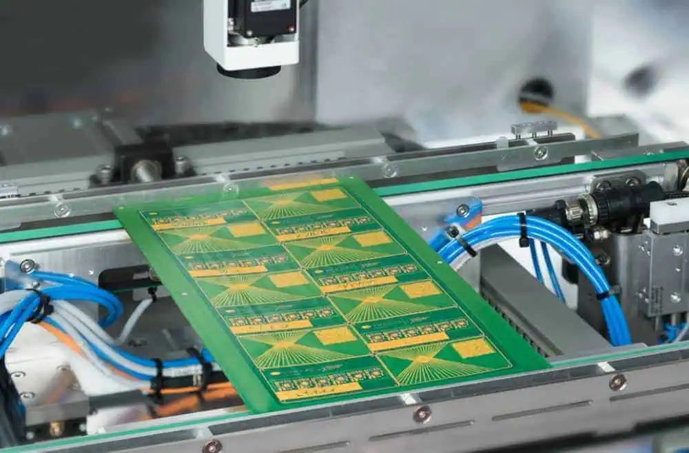
Different producers use different ways to label PCBs based on their priorities for quality, cost, and time. We want to tell you that laser marking machines are the best way to mark PCBs because they are affordable, work well, and are easy to use, and the labels will last a long time. They are better than other labeling methods. 

How to Make a Custom Laser Engraving Circuit Boards?

laser-cut-pcb

Tools & Materials

  • 10W laser. It was utilized to draw the circuit onto a plain copper printed circuit board using a printer. 
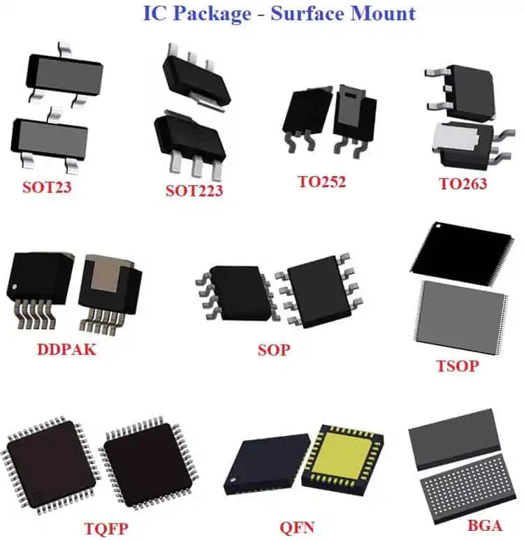
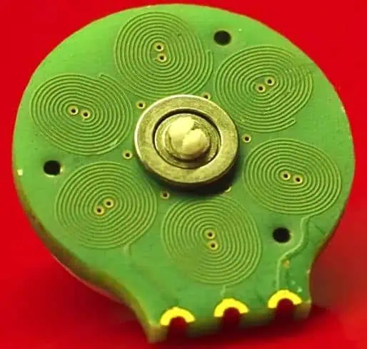
  • Copper PCB. The entire surface of the circuit board is covered with copper on one or both sides. Copper can conduct electricity, but the phenolic material underneath cannot. By removing pieces of copper coating, people can create pathways between the elements and make the printed circuit board.
  • Paintbrush. To cover the printed circuit board, a dense coating of paint will be needed, & a paintbrush will be helpful for this task. 
  • Ferric chloride. The material that you need to use comes in the form of salt, and you have to mix it with water before using it. This liquid can damage copper by taking it off its phenolic base. When you put on a mask, only the areas of the plate not covered by the show will be removed by the solution.
  • Sandpaper. Lastly, it would help if we eliminated any leftover masks on the board. You can do this easily by using sandpaper.

PCB Assembly or Manufacturing Process

The process of making homemade printed circuit boards usually involves the following steps. 

  • Designing

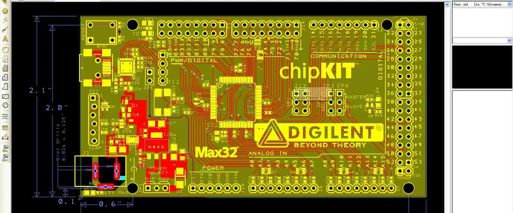
In the first step, a drawing is made of the circuit board that will be created. You can either design the new circuit board or copy an open-source project. There are different computer-aided design (CAD) software options you can use, such as Fritzing, Proteus, KiCad, Eagle, and more. 

  • Masking

After designing the PCB, the design transferred onto the actual circuit boards. There are various ways to create the circuit, like using heat to transfer toner from paper, drawing it by hand with a special pen, or utilizing a 3D printer.

After transferring the mask onto the board, the components of copper are eroded to remove them. By the end of the procedure, the circuit board must only have the pathways that create the circuit. 

  • End Finishing

After the corrosion process, The board will be prepared to be cleaned and drilled and have components soldered onto it. After that, you must check everything, turn it on, and be satisfied. 

PCB Designing & Mask Creating Process

FULL PCB MANUFACTURING Quote

After creating a printed circuit board design utilizing the CAD software you prefer, you can save it as an SVG file to open in graphic designing software. Different coatings can be sent, such as the bottom view, top view, silk, mask, etc. You can also choose between normal/mirrored formats for each layer. To follow the process described, you need to apply a disguise to the printed circuit board.

The board part protected by the mask won’t rust and will stay on the final circuit board. The features of the committee that aren’t covered by the cover will be open to the iron chloride, which will rust and eliminate them from the board.

To create the PCB in this procedure, you must cover the entire board with a paint coating and use a laser engraver to remove specific sections. 

To follow this method, you must invert the mask’s colors generated by most software (switch the black and white pixels). To do this, you can use two different software programs

  • Inkscape: One software is utilized to change SVG into PNG, and it can also be used to turn the design into a black&white image if it was exported from the CAD software in color format.
  • Gimp: Different software is used to change the mask’s color (turn white pixels to black pixels), and then the picture is added into the laser cutter software to be printed onto the plate’s surface.

Preparation of PCB

To start making the PCB, first, you need to apply a paint coating on the plate. A black water-based PVA paint is used, as a laser can quickly burn it. It is important to use dark paint as white paint reflects the laser and makes it less effective. 

It is necessary to use water-based paint because it can be removed from the board easily after the copper board has been etched.

To begin the PCB production process, a paint coating is applied on the plate in a single, uniform layer. The entire surface should be covered without any holes/imperfections, which could cause damage to the tracks or create undesired points of contact. It is important to use dark water-based paint, which can be easily removed from the plate after the copper board has been etched. 

It will help if you let the paint dry entirely before moving on to the next.

Engravings of Laser

After the paint has completely dried, the laser cutter can be used to remove the parts of the mask that are not needed. 

As mentioned earlier, a 10-watt laser cutter was utilized in this tutorial. 

If you use different equipment, you must try different combinations of such parameters to get the best outcomes. The laser does not have enough energy to make a hole in the copper plate, but it can remove paint and reveal the copper coating beneath it.

After using the laser engraver to remove the unwanted parts from the mask, it is essential to check if the circuit is printed on a board. This is because the laser can only deduct the paint, exposing the copper layer under it, and only the piece of the copper will rust. Remember that the dark parts will remain on the board after the corrosion.

The laser engraving process can take a long time, especially for larger boards. To speed up the process, it is recommended to only engrave the vital areas by using a tool in the CAD software that fills in the copper areas that do not need to be reduced. This will help to limit the quantity of paint that needs to be burned off by the laser. Otherwise, you will waste time removing the paint from unnecessary areas of the circuit board which are not part of the circuit. By reducing the quantity of copper removed by corrosion, the lifespan of the corrosive solution increases. This means that more prototypes can be made before the solution needs to be replaced.

Be careful not to print for too long, as the manufacturer suggests. It’s essential to take breaks of ten minutes as my printer recommends. 

Etching of Chemicals

After printing the mask onto the plate with black lines to protect the areas that should stay and uncovering the copper that needs to be eliminated, you can use ferric chloride to corrode the copper. This process usually takes some minutes until all the unwanted copper is eroded. Check the plate occasionally to see if all the unwanted substances have been eliminated. It usually takes around 5 minutes to remove everything, but checking is essential. You can gently pour some water on the plate (without rubbing it) to see the result better. Also, it’s a good idea to shake the ferric chloride solution occasionally to make it work better. 

Removing the Mask & End Finishing

After the rust is finished, you need to remove the leftover mask. You can use a brush & running water to do this. If you want a smoother finish, use sandpaper to eradicate the cover. Sandpaper is quicker and can make the surface look shiny and smooth. 

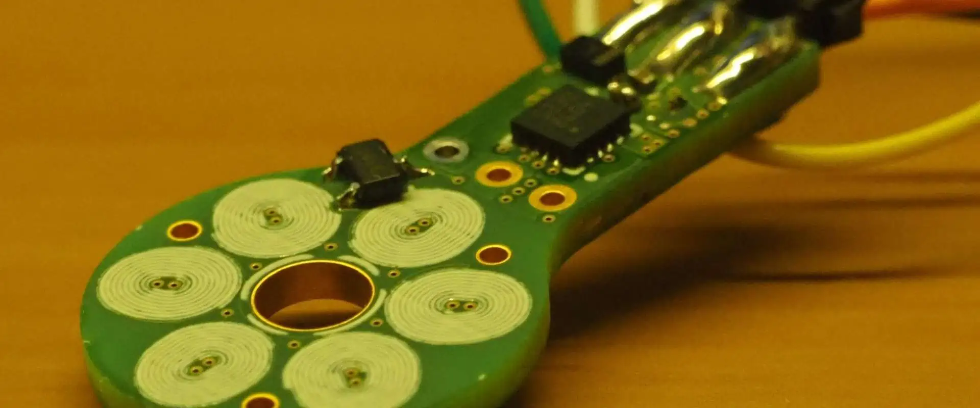
When you’re finished, the circuit board should only have the copper pathways needed for the circuit. Drill the circuit board to make holes for the components, then sell everything together. Congratulations, you’ve made your first PCB utilizing a laser cutter( engraver ).

Benefits of Integrating DesignSpark PCB Library

Designspark PCB library

PCB design software applications are available in a wide range. These applications help PCB designers carry out their design process easily. While some PCB design software applications require payment and subscription, some applications go for free. A good example of a free online PCB software is the DesignSpark PCB software.

Since the release of DesignSpark, RS has continued to upgrade some features so as to enhance its functionality. Users can have free access to this software since registration is absolutely free. Also, this software offers a variety of charge design resources and tools that transforms your ideas into a real circuit board. To have a good knowledge about the DesignSpark PCB software, read this article further.

YouTube video

What is DesignSpark PCB?

Designspark PCB

DesignSpark PCB is a free online design software package for circuit boards. This PCB design software is available on Windows. It is designed by RS components. As an award-winning electronic design automation (ECAD) software application, DesignSpark has got so many advanced features that help you have a lovely experience with PCB design.

DesignSpark PCB is a product of a partnership between RS components and Number One Systems. The projects in this software helps designers to organize design files. There can be several schematic sheets in a project. Furthermore, this software features a schematic editor. A particular project can feature several schematic sheets that help to create a complete design.

Since the release of DesignSpark, RS has continued to upgrade some features so as to enhance its functionality. Users can have free access to this software since registration is absolutely free. Also, the DesignSpark library features several footprints which helps you achieve a successful PCB design

DesignSpark PCB is available in various versions. The most recent version of this design software is DesignSpark 9.0. This version is available to online engineering community. This version has several upgraded features. Also, it includes the capability to identify dangling connections, create new libraries, and include copper pour to a net.

DesignSpark PCB includes tools like autorouter. The autorouter positions tracks between electronic components on a circuit board layout. This process is usually carried out automatically. Furthermore, DesignSpark PCB can help designers to generate Excellon drill files and Gerber Files. This software helps to bridge the gap that exists between high-cost PCB design software for professional design engineers.

DesignSpark PCB is designed to help PCB designers explore more advanced design options, thereby offering increased innovation. This features a sophisticated software engine that helps in capturing schematics and designing PCB layouts.

Features of DesignSpark PCB

FULL PCB MANUFACTURING Quote

This PCB design software features some specialized tools which helps professional designers manage and customize large projects that involve multiple layer circuit boards.

Variant manager

This helps you to define various designs to meet the requirements of the global market. With this feature, designer can add and configure variants of PCB board design. It enables you to design special values for the similar component parameters in several variants.

Panel design editor

DesignSpark PCBโ€™s panel design editor helps you manage and visualize assembly of finished board designs before manufacturing begins. Panel editor helps you create panel layouts for your circuit board. Also, this feature enables you to view the panel on-screen.

Hierarchical schematic design

Hierarchical schematic design enables you to split schematics in building blocks. This feature helps designers to use block symbols to represent various schematic designs. The hierarchical schematic design in DesignSpark PCB offers you a more efficient method to organize your circuit board designs. In this case, the designer may have a top sheet that comprises block symbols which represent the subcomponents of your PCB design.

Advanced routing modes

DesignSpark PCB features advanced routing modes which offers designers the capability to route complex circuitry required for new PCB. This feature helps designers achieve complex PCB trace routing.

Configurable design rules editor and checker

DesignSpark PCB offers a fully configurable design rules checker which helps you verify the design of a circuit board and pass on quality checks for manufacturing.

Dual screen support

Another important feature PCB designers will enjoy from DesignSpark is its support for dual screen. This software supports dual screen while working on it.

Benefits of Using DesignSpark PCB

The DesignSpark PCB has several benefits. In fact, designers have a lot of benefits to enjoy.

Unlimited schematic size

Printed circuit boards are available in various shapes and sizes. These boards offer various purposes. Irrespective of your circuit boardโ€™s size, DesignSpark offers you the freedom you need when designing your schematic. With this PCB design software, there is no limitation on the size of your schematic sheets. Also, this flexibility and freedom enables designers to integrate Design Spark PCB for any size of PCB projects.

Embedded DesignSpark PCB library

The DesignSpark library has several features. One of the numerous benefits of using DesignSpark PCB is that it allows you to create the footprints and symbols according to industry standards. Furthermore, the ready-to-use libraries help you easily create these footprints without much stress. Designers can as well design their own part models based on their specifications. The ready-to-use online tools will help you get the models of the parts needed.

Create BoMs in your desired format

You can prepare BoM that features items and parts you want in your preferred format. Also, you can order parts easily at your own time. DesignSpark features a built-in BOM Quote functionality that enables you to achieve this. Just upload the Bill of Material to the RS Components website.

Unlimited PCB design

Another important benefit you can enjoy from the DesignSpark PCB is unlimited PCB design. Some circuit boards design requires about 50 layers. However, not all software enables that. The DesignSpark PCB enables you to integrate the number of layers your circuit board needs. Also, these software offers no limits as regards the highest number of pads or nodes. There is also no limitation on the number of connections.

Enables export to Spice Simulation software

DesignSpark PCB schematic capture environment includes the LTspice simulator. This increases the possibility to execute circuit simulations. Also, this enables designers to easily export your project quickly to Spice Simulation.

Output the needed files

With the DesignSpark PCB, designers can easily prepare unlimited fabrication files such as ODB++, Berber, or IPC to order circuit boards from their preferred manufacturer.

Free online software

Another benefit of using DesignSpark PCB is that you donโ€™t need to pay any amount to have access to this software as it is completely free. It is a free online PCB design software specially designed to meet the requirements of various users.

What does the DesignSpark PCB Library Offer?

Altium PCB design process

The DesignSpark PCB library offers designers a lot. This embedded library allows designers to browse already stored footprints. Also, the library comprises PCB footprints that are representation of other mechanical characteristics and the physical pad arrangement of components.

This library is ideal for managing components. Also, this library is specially designed to meet the requirements of various users. As a huge and embedded library, there are several footprints included in it. Also, this library is very easy to use.

DesignSpark PCB users can have access to numerous design tools like:

DesignSpark Mechanical: This sophisticated 3D CAD tool works according to direct modeling techniques.

DesignSpark Toolbox App: This IoS and Android app is ideal for engineers. It includes comparison tables, calculation tools, and more.

DesignSpark Electrical: This particular electrical CAD package for designing electrical and machinery systems and a design of control panel.

Obsolescence manager

This tool allows engineers to control and review the status of products within BoM and choose alternatives.

Frequently Asked Questions

What type of users and organizations can use DesignSpark PCB?

DesignSpark PCB is great software ideal for organizations like small business, freelance, and mid size business.

What is the highest number of pads or nodes when designing with DesignSpark PCB?

There is no maximum number of pads you can use when designing DesignSpark PCB. This software offers you the freedom to use the number of pads you want in your design.

Is DesignSpark PCB free?

This online software requires no charges. Another benefit of using DesignSpark PCB is that you donโ€™t need to pay any amount to have access to this software as it is completely free. It is a free online PCB design software specially designed to meet the requirements of various users.

Conclusion

Whether you are in need of a standalone design tool or a good design ecosystem, DesignSpark PCB is a complete design package you can seamlessly integrate in your existing design workflow. With the software, youโ€™ll be able to have freedom to create your schematic as there is no restriction on the size of your schematic or number of schematic sheets.

Also, this PCB design software package offers freedom and flexibility to integrate as many layers as you want in your PCB design. It is an easy-to-use software that offers great features to help you transform your creative design into a real board. As the most comprehensive and accessible PCB design software in the world, you can easily and quickly transform your ideas into testable boards.

How to Check Circuit Board Components

components manufacturers

Major components included in practically every electrical instrument as well as electronic devices are circuit boards. It has radically altered the globe for all time. Even when a circuit board also isn’t required for technical purposes, operating with a defective one is typical. Every engineer at one time has been in a dangerous situation, where they managed to survive.

It is crucial to learn how to inspect the circuit boards for errors in order to effectively use the instruments. Due to the diversity of the components that make up circuit boards, there may be some flaws in the board diameters.

Fluid leakage, burned circuit components, power-related concerns, soldering errors, including connection shorts on PCBs are among the prevalent failures on the circuit boards.

Despite the seemingly lengthy list, you may rapidly verify these issues using the multimeter. As a result, we will talk about how to inspect the Board for electrical faults using the digital multimeter. Let’s think about numerous approaches of testing and how to check circuit board components.

Checking Faults in the Circuit Board Components

These are some crucial actions you may do to test the circuit boards. Locating damaged components on the circuit board; detecting short circuits in the PCBs; testing for any short circuit present on the electronic boards;

Locating PCB short circuits or other circuit board flaws

The multimeter seems to be a trusted tool for identifying shorts as well as other technical defects in virtually any electrical device. A circuit board can be quickly checked for capacitance, current, input voltage, DC & AC voltage, resistance, fuse shorts, with a multimeter.

The tool is typically thought of as a mixture of the ammeter, voltmeter, and multimeter because of the way it performs numerous circuit board testing tasks simultaneously. It’s crucial to try various examination techniques first before turning to multimeter probes to locate electronic issues. Let’s think about them.

Vision examination

If, after the breadboard design stage, the circuit breaker isn’t really present, the first thing you should do to find any short circuits on a PCB is to thoroughly examine the entire PCB surface.

Also, if one is available, utilize a low magnification microscope or magnifying glass throughout the examination; this is how to check circuit board components.

Look for the tin whiskers between both the solder pads or joints starting with the supply of power. Solder lumps or cracks should draw your attention when you see them. If you requested unplated vias, make sure they are present throughout the vias, and the same is true of the circuit boards. Poorly plated vias can assist in the formation of short integrated circuit present in between these layers, now that everything is connected to ground, VCC, or both.

You will notice some charred patches on the component whenever the short gets too serious and causes components to achieve critical temperatures.

Comprehensive Physical Inspection

FULL PCB MANUFACTURING Quote

A thorough physical examination will also provide you with some important and applicable insights about a broken circuit board. It’s also helpful in locating the defective parts that you would not often be able to locate through just visual inspection. You can use an oscilloscope to achieve better results.

Infrared Imaging

You can find places where there’s significant heat generation by using an infrared camera. Also, even if the short is seen between internal layers of the circuit board, there’s a likelihood of having one when you’re not observing hot areas far from active components.

The resistance of the short is typically higher than that of the solder joints or an ordinary trace. This occurs because it fails to benefit from the design’s optimization. Because of this resistance and the high current which results from the ground and power lines’ direct electrical connections, the conductor found in the PCB short circuit will eventually become heated.

Start with the smallest current possible. Ideally, you’ll catch this short even before it causes additional harm.

Checking Electronic Circuit Boards Components for Any Short Circuit

Other than visual inspection, you can find various approaches to identify the main reasons for a circuit board short circuit.

Testing of circuit boards components Using the Digital Multimeter

You must examine the recognized resistance existing between the various circuit locations on the circuit board in order to test it for any short circuits. But, if the visual examination is unable to provide any information regarding the location or origin of the short circuit, obtain a multimeter, then try locating the Board.

Online, particularly in most of electronic forums, this multimeter method typically elicits a variety of conflicting reactions. Nonetheless, tracing the short circuit’s test locations might be quite helpful in identifying the issue.

The multimeter you use in this situation needs to be milliohm sensitive. It would also be fantastic if it could warn you the moment you begin investigating shorts.

For instance, when measuring resistance between adjacent traces or pads on the circuit boards, high resistance must be measured as well.

Finding Grounds on the Circuit Boards

The fact that this situation concerns the grounded plane as well as grounded via is a crucial one. Return pathways will be present on multilayer Boards with internal ground planes. The vias and pads on the surface layer of the board are best inspected and verified in this area. Place a probe upon that board’s ground connection then afterwards touch the remaining probes to the other conductors of the board.

Moreover, other locations of the board will also have the ground connection. This indicates that when each proof is applied to two different and grounded vias, you will only detect a very modest resistance. Take note of your layout when trying to do this; you wonโ€™t want to have errors.

Shorted Components

This indicates you are using the multimeter to measure the resistance while you’re looking for defective or shorted components. If a component’s visual inspection will not really show any additional metallic solder or flakes between the pins or pads, the short might well have formed in the interior layers between both of them.

Poor fabrication practices can also result in shorts, which is another reason circuit boards need to go through DFM and design rule checks. Pads and vias put close to one another may unintentionally short or bridge when being manufactured.

You will need to gauge the resistance between those pins of a connection or IC in this situation. Moreover, close-spaced pins usually experience shorts.

Additionally, shorts are frequently caused by pins that are close together. Shorts could still develop in other places, though. Verify that there’s a minimal resistance between the pads/pins and ground connection, as well as between them.

Limit Your Search Area

When you believe you have discovered shorts between two conductors as well as between earth and a particular conductor, you should focus on the neighboring conductors to pinpoint their location.

Locating Defective Parts on the Printed Circuit Board Components

The board may experience issues due to faulty or poorly placed components. It’s possible that these parts are defective or fake. This produces the look of shorts.

Faulty components

There is a chance that some parts could go bad overnight. The electrolytic capacitors forms a prime illustration of this. Check any component that you suspect first if one is present. Now, if you’re unsure, you can search for any component that you believe failed on Google. Moreover, see if the problem is a regular one.

You might have short circuits as a result of the burned-out component in situations where you detect an incredibly low resistance between the two pads/pins. This warning plainly shows that such a capacitor is defective. Moreover, capacitors swell whenever they are damaged or when the voltage applied exceeds the necessary level.

What to Do If a Circuit Board Component Is Faulty?

Shelf Life of Electronic Components

Utilizing a defective circuit board component or printed circuit board component could be dangerous for different devices.

As a result, you might need to either repair or replace the damaged or defective circuit board. As stated by the EPA, the main purpose of this is to prevent dangers from these broken pieces. Thus, hiring a qualified electrician to help you replace the circuit or copper traces with shorts is strongly advised. This guarantees that the device operates properly.

Conclusion

Learning how to check circuit board components is easy. This is why we have explained the process. Fluid leakage, burned circuit components, power-related concerns, soldering errors, including connection shorts on PCBs are among the prevalent failures on the circuit boards. Smaller copper trace is typically used to make printed circuit boards. Moreover, accuracy is employed during the connections. As a result, even a very small flaw can completely destroy the device. It’s one of the reasons why it’s important to learn how to inspect such integrated circuits and circuit board components for errors in order to ensure the user’s safety and that these electrical devices function properly. Once you identify the issue successfully, you might either find solutions to it by yourself or get an expert in the field to assist you.

Everything you need to know about Keypad PCB

keypad PCB

If you are an engineer, gamer, or hardware enthusiast, you have probably heard of or come into contact with a keypad-printed circuit board. However, these keypad PCBs often present themselves in a manner that makes them feel and look like complex components. Therefore, most people in the tech industry usually prefer to purchase ready-made keypads instead of producing their own. But what if there was a way to produce your keypad-printed circuit board?

A keyboard-printed circuit board sets aside the mechanical keypad from a regular keypad. Therefore, no matter the type of keypad you are planning to generate, a traditional membrane or mechanical keypad, you’ll need in-depth knowledge of the different kinds of keypad printed circuit boards. Moreover, you should be able to answer simple questions such as, what is a keypad PCB? What is the difference between traditional membrane keypads and mechanical keypads? And so much more.

What is a Keypad?

keypad board
keypad board

Keypads are generally sets of keys or buttons bearing digits, alphabetical letters, and/or symbols placed in perfect order on a simple pad. These components are usually utilized as input devices on various gadgets, which include personal computers or PCs.

Keypads can bear numeric digits exclusively; for example, keypads found in calculators or digital doors. Moreover, they can also bear alphanumeric values, for instance, the keypads on various cellular phones.

Desktop computers mostly come with keyboards with various keys that users utilize to input data onto a computer. For instance, a standard desktop computer keyboard comes with two variations of input keys for numerical digits:

  • One variation is found on the upper part of the keyboard in row-form
  • The second variation is on the right portion of the keyboard, and it tends to be more efficient in terms of data entry

However, for more compact computers, for example, notebooks and laptops, users sometimes have to insert external plug-in keypads to gain all the features that come with the standard desktop keyboard.

Keypad Printed Circuit Boards in a Nutshell

A keypad-printed circuit board is basically a sheet or a panel in a PC that acts like the keypad’s foundation or main component. Typically a keypad printed circuit board senses and defines whatever happens when users press keys in a keypad.

Using a keypad-printed circuit board, you can easily determine the key that was pressed on the computer. Moreover, you can also transfer information to your PC using the keypad in a matter of seconds.

A keypad has two main parts, which are the following:

  • The physical keys โ€“ these are the keys that the users see
  • The controller part โ€“ this is the part that carries out all the processing. Unfortunately, it is usually in the background; therefore, users can’t see it while using the keypad.

Most technicians use thin plastic sheets and metal or epoxy components to generate keypad circuit boards.

Main Differences between membrane and Mechanical Keypads

FULL PCB MANUFACTURING Quote

Membrane and mechanical keypads have multiple differences, which include the following:

Size and Cost

Membrane keypads, which also go by the name traditional keypads, are generally light and affordable. On the other hand, mechanical keypads are bulky and expensive.

However, even though membrane keypads are affordable and lightweight, they tend to have a shorter life span when compared to mechanical keypads.

Operation

Membrane keypads have rubber underneath. Therefore, you get a mushy feel whenever you press a key when using this type of keypad. Moreover, this rubber feature makes these keypads relatively silent. On the other hand, mechanical keypads have spring-loaded switches beneath the keypads that effectively trigger whenever you press a key. As a result, mechanical keypads tend to respond with pretty loud clicking sounds.

Feedback

Due to the design of the mechanical keypad, it provides more efficient feedback compared to the membrane keypad.

Rollover

Mechanical keypads tend to have a vital feature known as rollover which helps them spot essential key presses simultaneously. Due to this feature, the mechanical keypad tends to be great in the following:

  • Fast typing
  • Playing games
  • Crouch jumping and much more

On the other hand, the membrane keypad lacks this crucial rollover feature. Therefore, these keypads tend to lag your input due to limited processing.

Pressing Power

When using a mechanical keypad, you don’t have to apply much pressure to the keys to input data. By gently clicking on the keypad keys, the board’s mechanism automatically detects the keystroke and registers it into the processing unit. However, when working with a membrane keypad, you must apply a lot of pressure on the keys to register the keystroke. That is because the rubber layers on the membrane keypad must touch the circuit for the data to be submitted effectively.

Customization

Mechanical keypads are super easy to customize, unlike membrane keypads which require a lot of effort and time.

How can you generate a Custom Mechanical Keypad?

In this section, we will effectively discuss all the steps you must follow to generate a custom mechanical keypad.

First, you’ll have to gather various components you will use on your mechanical keypad. These components include:

  • A printed circuit board
  • USB cable
  • Keycaps
  • Case and back plate
  • Keypad switches
  • Stabilizers

Combining the Parts

To combine all the parts and generate a functional keypad, you should follow the following steps:

  • First, check whether or not the keypad printed circuit board is working.
  • Next, carefully mount the keypadโ€™s cherry stabilizer on the circuit board.
  • After attaching the keypad’s switch to the circuit board, flip the printed circuit board over and solder the components.
  • When the soldering process is over, you must connect the keycaps.
  • Once you are done mounting the keycaps, you can move on to the testing phase, which involves testing the keypad to ensure it is functioning according to your specifications.

To test the keypad, connect it to your PC using the USB port, then check whether the keys function accordingly.

Conclusion

Keypads are vital components in any desktop, laptop, or simply any computer setup. Without a keypad, users can’t be able to input critical information into a computer. Moreover, the entire industry shifted since keypad-printed circuit boards hit the market. These components basically make keypads more efficient compared to traditional membrane keypads. Therefore, if you want to try out keypad-printed circuit boards, we hope this article has helped you with all the information you were looking for regarding keypad PCBs.

How Toย Order PCB with componentsย in the Right Way?

The contents of this repository comprise all the necessary files for the production and assembly of b-parasites. Typically, the fabrication process involves placing an order with a company capable of manufacturing the PCB and performing surface mount technology (SMT) assembly, which consists of mounting various components such as capacitors, resistors & oscillators. This page overviews the required files, functions, and locations. 

PCB manufacturing headaches are universally disliked, but there are numerous steps you can take to ensure a smoother production process. By adhering to the following printed circuit board production advice, you can reduce costs, minimize production faults, and enhance the overall quality of your PCBs. 

If you have never ordered Printed Circuit Boards for the product before, the process can be pretty daunting. 

If you are delegating your electronics layout to an outside engineer, they will typically handle most of this process for you. However, if you plan to undertake this task independently, you will quickly realize that numerous intricate terms & specifications require your comprehension. 

Regardless of your approach should possess, at the bare minimum, a fundamental comprehension of the prerequisites to order new PCBs. 

This article aims to dissect all of the specifications & terms to assist you in comprehending the different tradeoffs. 

While certain manufacturers may employ unique terminology for these specifications, most will apply universally, regardless of the location where you order circuit boards. 

Basics of Ordering Printed Circuit Boards

Order Quantity
Order Quantity

Creating a fully functional PCB comprises two primary phases: the production of the bare board and the subsequent soldering of all the elements. This article categorizes all the diverse specifications into two stages. 

To order the printed circuit board fabrication for the bare boards, you must provide the producer with Gerber files, which are made from your printed circuit board layout software. 

To facilitate the printed circuit board assembly process, you must provide the manufacturer with a BOM that contains a comprehensive list of all the components. Additionally, a file must be submitted, which includes the exact coordinates of each element that will be employed to program their soldering device. Your printed circuit board layout software creates these files. 

PCB with Components

Standard Specifications

  • Board type: Typically, you will opt for “single pieces” when placing your order. PCBs are not created individually but produced in large panels with many copies of the circuit board. This approach allows for better production of smaller committees. Following the printed circuit board assembly or final testing, the boards on every panel are depaneled. 
  • In the majority of cases, penalization will not be a concern for you, as the producer will provide you with fully assembled PCBs that have been separated. 
  • Different Design in Panel: It is feasible to consolidate various boards on the already present panel. Whether your product necessitates multiple boards, you can place them all on a single panel to reduce costs. However, there is an extra charge for a discussion with diverse board designs.
  • Size: If you are ordering single pieces, the dimensions of the PCB are a crucial factor in determining the printed circuit board cost. Alternatively, if you order panels, the panel dimensions will play a significant role. 
  • Quantity (single): Commence with five boards for your initial version, and gradually escalate the amount as the confidence in the layout improves.
  • Layers: The number of routing layers utilized in your printed circuit board design is a crucial factor. Apart from a single layer, it is typically an even number. A basic PCB design employs 1 to 2 layers. Most moderately complex structures, such as those containing microcontrollers, require four to six layers. In contrast, more intricate designs, like those containing microprocessors, necessitate eight layers. The no. of layers directly impacts the price of the printed circuit board. 
  • Material: The base substance employed in the printed circuit board between stacked layers is the substrate. FR-4 is the most widely used substrate material, which is adequate for most layouts. 
  • FR-4 is available in various Tg versions, where Tg denotes the transition temperature. It indicates the temperature or heat at which the substance loses its rigidity and becomes more flexible. For most layouts, TG150-160 is the suitable choice without any additional cost. However, upgrading to TG170-180 results in a significant cost increase. 
FULL PCB MANUFACTURING Quote

If your design comprises custom RF circuitry, including transmission lines, you may require an RF-specialized substrate material. The substrates from the Rogers R4000 series are widely utilized for RF designs. The R4003C substrate material is halogen-free and more eco-friendly compared to R4350B. Both materials exhibit comparable RF-related specifications.

If your design necessitates effective dissipation of heat, a substrate with a metal core may become imperative. This is exceptionally ordinary in high-power applications, such as LED lighting.

An HDI board is a type of printed circuit board that has a higher trace density, miniaturized features, and more layers than a commonly printed circuit board. This advanced technology is typically used for very complex or small layouts, and it can be considerably more expensive than a standard printed circuit board. 

Buried vias and Blind vias are typically utilized when mini size is essential as they increase the cost of the board. In comparison, standard vias are PTHs, meaning they traverse through all layers, even if they are unnecessary on particular layers. Standard vias connect through all layers of the PCB, even when they are not required on specific layers, taking up extra space. Conversely, a blind via establishes a connection from an outer layer to the inner layer and is solely visible on one terminal of the ultimate board. A buried via connects between two inner layers and is completely invisible on a final circuit board. Both blind and buried vias are used when space is critical, but they significantly increase the board’s cost. 

  • Thickness: The board thickness is the final dimension of the PCB. The most commonly used density is 1.6mm. If space/weight is a critical factor, then a thin board would be preferred. On the other hand, if the strength of a circuit board is a concern, then a thicker board would be the best choice. 
  • Min track / Spacing: This refers to the minimum width of routing traces or tracks and the less space allowed between them, measured in miles. The standard minimum width is six mils, but in layouts where the area is essential, the minimum width may be reduced to 3-5 mils. However, going below six mils will significantly increase the price of the board. 
  • Min hole size: The minimum size of the hole refers to the minor diameter that can be pierced on the PCB. This is particularly relevant for creating vias that route connections between layers. A smaller hole size can allow for tight packing of elements and reduce the amount of space taken up by the vias. 
  • Solder mask: The solder mask is like a coating that is put on the top and bottom layers of the board to protect against oxidation and prevent solder bridges between adjacent pads. Although green is the most ordinary color, you can choose other options. 
  • Silkscreen: Silkscreen is the coating that allows you to add text and basic images, such as logos, to your circuit board. Its primary use is to indicate component identifiers. 
  • Gold fingers: If your board includes edge connectors, it is recommended to opt for gold plating to enhance corrosion & abrasion resistance.
  • Surface finish: The surface finish is a coating that is put on the metal pads on the outside layers of the PCB to make it easier to attach components and protect them from damage caused by rusting. Previously, Hot Air Solder Leveling (HASL) was the most widely used surface finish, but it has now been replaced mainly by Immersion Gold (ENIG) due to its lead-free nature. Immersion Silver is also a non-toxic option for surface finishing. 
  • Via Process:ย Typically, the vias remain unsealed, but there may be situations wherever you need them to be shut. Tenting the via is the simplest & most cost-effective option, as it covers the via with a solder mask coating. However, tenting works best with minimum diameter vias.
  • Sometimes, when Ball Grid Array packages are very close together, the tiny holes called vias near the chip pins can cause problems with soldering. This can result in bad connections between the chip and the circuit board. To fix this issue, the vias can be filled with a material to prevent the solder from being drawn away from the chip pins. This solution is more expensive but necessary in some cases. 
  • Finished copper weight: The copper weight measures how much copper is on each square foot of a circuit board. It tells you how thick the copper is. When we say 1oz of copper, the copper is 1.4 thousandths of an inch thick. In designs with a lot of power, thicker copper makes narrower paths for the current to flow through. This specification is essential for the outside layers of the circuit board.
  • Inner copper weight: It is the weight of copper (as described in the Finished copper weight section) for the interior layers of the board. It is generally recommended to route significant current traces on the exterior layers of the board as they offer excellent heat dissipation

PCB Assembly with Components

through-hole assembly process

Standard Specifications

  • Component sourcing options: There are three options available: Turnkey, Kitted, or Combo. Turnkey involves the supplier sourcing and providing all components, Kitted requires the customer to provide the features, and Combo is a blend of both Turnkey and Kitted options. 
  • Board type: This option determines whether the boards will be assembled individually or as some panel. If the board count exceeds twenty pieces or the board size is smaller than fifty million meters per side, penalization is recommended to optimize the production process for efficiency. 
  • Quantity: 
  • This refers to the number of PCBs that will be assembled separately
  • The number of Unique Parts: This indicates the number of distinct elements that will require soldering on your PCB. For instance, if your layout utilizes five identical capacitors in different locations, it would be considered one unique element. This count encompasses every discrete chip, resistor, inductor, capacitor, connector, etc. 
  • Several SMT Parts: This refers to the number of elements necessitating Surface-Mount Technology. This count encompasses all components, not unique. For instance, if you have identical SMT capacitors, it would be counted as 5 SMT parts. 
  • Many Through-Hole Parts: This indicates the number of components necessitating the through-hole manufacturing procedure. PThs parts are infrequently used in contemporary electronic designs, except when a more robust attachment is required, like for the connector that will endure recurring forces.

Conclusion

Suppose you’re interested in ordering expertly created boards, whether in small numbers for prototyping or larger volumes for creation; my preferred manufacturers include PCB way, Seeed Studio & Bittele, located in China. For manufacturers located in the United States, I would recommend Sunstone Circuits Board.

While you also have the option of manually assembling your boards, I usually don’t advise it unless you possess advanced soldering skills. Most modern microchips are not amenable to manual soldering.

Another major drawback of manual soldering is that if you encounter issues with your layout, it can be difficult to distinguish between poor soldering and fundamental layout problems. By procuring boards & assembly services from an expert manufacturer, it will considerably make simple the testing and debugging of your layout.

While there are numerous technical things that you should be familiar with to place an order for PCBs, this article hopefully assisted you in comprehending those prerequisites more thoroughly.

How to calculate PCB design cost?

Altium Designer 20

Printed circuit board (PCB) design is a complex process involving many steps like schematic capture, board layout, DFM analysis, prototype fabrication and assembly. Estimating an accurate PCB design cost is important for budgeting any new electronics hardware project. This article will explore the key factors that contribute to overall PCB design costs.

Types of PCB design costs

The main components of PCB design costs are:

Engineering costs

  • Schematic design
  • PCB layout
  • Simulation and analysis
  • Component selection
  • Design reviews and documentation

Prototype fabrication costs

  • Board materials
  • Number of layers
  • Board size
  • Line width and spacing
  • Special processes like impedance control
  • Testing
  • Shipping

Assembly costs

  • SMT programming
  • Component cost BOM
  • Placement and assembly
  • Test and inspection

Tool costs

  • EDA software licenses
  • Library costs

Other costs

  • Communications like conferences calls
  • Travel and expenses
  • Project management

Key factors impacting PCB design cost

Below are some of the main considerations that affect overall cost:

1. Complexity

More complex boards take longer to design and cost more. Factors adding complexity:

  • Component density and pin count
  • Number of unique parts and BOM line items
  • High speed signals requiring impedance control
  • Small board size relative to complexity
  • Multiple voltages and power domains
  • Layer count
  • Mixed-signal content – analog and digital

2. Design quality

Higher design quality results in fewer spins and reduces overall cost. Parameters indicating quality:

  • Schematic completeness and consistency
  • Layout precision and manufacturability
  • DFM analysis like thermal, signal integrity
  • Test point inclusion
  • Documentation

3. Prototypes and spins

Multiple prototype iterations add cost but reduce long term risk. Consider:

  • Number of prototype builds
  • Quantity per build
  • Design or fab driven spins

4. Certifications

Certification requirements like UL, CE increase design time and prototype costs.

5. Volume

Amortize NRE costs over total production volume. High volume reduces per unit cost.

6. Schedule

Faster time to market has higher engineering costs for resources and tools.

7. Support

Post design support like fab liaisoning, assembly support, DFM review adds cost.

8. Team location

Labor rates vary based on geographic location.

PCB design cost estimation methods

Below are some methods to estimate PCB design costs:

1. Historical data

Leverage costs and metrics from similar past projects of known complexity and scope. Adjust to account for differences.

2. Vendor quote

Get budgetary quotes from vendors outlining their cost structure. Compare multiple vendors.

3. Estimation by hour

Estimate hours needed for each task and multiply by hourly rate based on complexity.

4. Cost per component

Estimate cost based on cents per component placed, adjusted for complexity.

5. Cost by board size

Estimate based on cost per square inches of board area. Adjust for layer count, density, complexity.

6. Cost by design phase

Allocate percentage of total cost to design phases – schematic, layout, prototyping etc based on project scope.

Cost driving PCB attributes

PCB Antenna Layout
PCB Antenna Layout

Below are some PCB characteristics that drive fabrication and assembly costs higher:

Layers

PCB TypeTypical Layers
Single sided1
Double sided2
Multilayer < 6 layers4-6
Multilayer > 6 layers8+

Board size

  • Minimum charges apply for small boards
  • Each additional square inch adds cost

Fine features

  • Tighter line width and spacing
  • Smaller vias
  • High layer to layer alignment

Materials

  • Standard FR4 cheaper than high frequency materials
  • Exotic materials like ceramic, Teflon costly
  • Thicker boards more expensive

Finishes and coatings

  • Immersion silver, gold, ENIG cost more than HASL
  • Conformal coatings add cost

High density

  • More components per area add complexity
  • 0402 vs 0603 vs 0805 size components
  • BGAs vs QFNs vs 01005 passives

Impedance control

  • Tight impedance tolerance layers like +/- 5% add cost

Testing

  • Test point access required
  • ICT, bare board testing
  • Flying probe, boundary scan techniques

Fab and assembly cost drivers

In addition to the PCB, fabrication and assembly processes impact cost:

ProcessCost driver
Solder maskTight tolerance on registration adds cost
Legend printMulti-color prints cost more than single color
Via fill/pluggingFilling unused vias
Gold fingersEdge connectors with gold plating
PanelizationTooling and handling for panel assembly
SMT programmingComponent packages, inspection programs
Selective wave solderAdditional process step
TestingInvestment in test fixtures and handling
Box buildFinal product assembly steps

Example cost calculation

Corne PCB Layout
Corne PCB Layout

Below is an example cost estimate for a hypothetical medium complexity PCB design:

PhaseHoursRateCost
Schematic design40$80$3200
PCB layout60$60$3600
Library creation10$40$400
DFM analysis12$50$600
Prototype fabrication$2000
Assembly setup$500
Test preparation16$45$720
Project management20$65$1300
Total$11,320

This provides an initial cost estimate that can be refined as details become clearer. Quote must be obtained from the fabrication shop and assembler for final pricing.

Conclusion

Estimating PCB design costs requires an analysis of the various cost factors based on design complexity, schedule, quality and prototype requirements. Allocating cost by typical percentages for each design phase also provides good budgetary guidance. The cost drivers outlined here help identify areas that can be optimized to reduce overall PCB cost and development risk.

Frequently Asked Questions

Pads Layout Viewer Download

Q1: What is the typical cost per square inch for 2 layer PCB fabrication?

For low to medium complexity 2 layer boards, typical cost per square inch is around $2 to $5. High complexity boards can be $6 to $10.

Q2: How can PCB design costs be reduced?

Cost reduction approaches include:

  • Simplify schematic and layout as much as possible
  • Use fewer layers
  • Reduce board size
  • Standardize on component packages and footprints
  • Reuse proven schematic blocks and layout patterns
  • Select standard materials and finish
  • Build sufficient DFM review time

Q3: Does PCB assembly cost more for BGA packages versus QFPs?

Yes, boards with many BGA packages often cost more to assemble than QFPs due to:

Q4: How much does fabrication cost reduce at higher volumes?

For volumes above 10,000 pieces, fabrication cost can decrease by 25% to 50% compared to low volume prototype pricing for the same PCB design.

Q5: Does prototyping PCBs in Asia reduce cost compared to North America?

Yes, typically assembly costs in Asia are 30-50% cheaper than North American vendors for low to medium volume batches. So prototypes assembled in Asia can reduce cost.

What is the Cost of PCB Layout Services

Pads Layout Viewer Download

Printed circuit boards, or PCBs, are vital components of multiple electronic and electrical products. These components connect various elements, and they function in everything from computer and DVD players to car engines and underground sensors. Moreover, printed circuit boards have been available since the second world war when governments were utilizing them exclusively for military applications. As of the 21st century, you can find these components in almost every electrical or electronic gadget that you come across.

However, this means that when you are developing an electronic gadget, you will likely require the services of a printed circuit board designer to generate your PCB layout. Moreover, you will probably need an electrical engineer to help you convert the design into a physical circuit board.

But, before you move on to the hiring stage, it is crucial to first figure out the average rates of hiring a printed circuit board designer for PCB layout services. Doing so will help you generate a reliable budget for your project. So how much does it cost to gain PBC layout services? And should you outsource the PCB layout development process or work on the project independently?

What you will need

Reducing PCB Design Risk-Layout

Even though you can quickly gain a rough estimation of how much it will cost you to hire a printed circuit board designer, for you to gain an official PCB layout quote, you’ll have to provide sufficient details about your board design to the circuit board engineer. After receiving this information, the circuit board design engineer will calculate how much it will cost you to generate the design and then provide you with an estimated price that is more accurate.

If you skip this step, your estimation may be inaccurate, leading to you going over budget.

When generating the PCB layout quote, you must provide some documents to the printed circuit board design engineer. Moreover, there are additional documents that you can also provide that, though optional, can help offer a more accurate estimation.

Here are the most common documents that youโ€™ll have to provide:

Schematic

The schematic is, without a doubt, one of the most crucial documents you must provide to the PCB design engineer. The documents should be in a PDF or Native design format for portability.

Generally, schematics tell printed circuit board design engineers a lot about your product, including the following:

  • How much effort will go into generating your circuit board layout design
  • How many hours will go into creating the layout design

Moreover, this document also gives the PCB designer a rough idea of the complexity of your PCB design.

Bill of Materials

The next document is the bill of documents, commonly known as the BOM. Generally, BOMs contain a list of all the parts and materials the manufacturer will utilize to generate your printed circuit board. Typically, you can take BOM as a complex shopping list containing all the elements that you’ll need to develop your printed circuit board.

BOM documents will inform the printed circuit board designer about the components you wish to use on your PCB.

Mechanical (simple X and Y dimensions, PDF, IDF, or DXF)

FULL PCB MANUFACTURING Quote

The last essential document you must hand over to the PCB designer is the document containing mechanical information. The mechanical info document typically includes details about the board’s outline and dimensions.

When it comes to this document, printed circuit board designers need all the information you can share, do not leave anything behind. That is because this information will help them design the PCB so that it will be functional and still fit impeccably into the product that you will use the circuit board on. Therefore, if you mess up this document, you might get an oversized or under-size printed circuit board in return.

These are generally the most crucial files that you have to share with your PCB designer for them to generate an excellent and accurate PCB layout. However, you can still add more details to help the PCB designer get your PCB layout quote more accurately. Moreover, this additional information will be helpful during the design process.

Some optional files that you can choose to share include:

  • Component datasheets
  • Placement floorplan
  • Constraint/routing rules
  • Netfiles

What next?

With these details, your circuit board designer will clearly see how your printed circuit board is supposed to look like at the end. Hence, they should be in a position to give you a close-to-accurate estimation of how much money you’ll have to spend to produce the PCB layout.

However, if you do not have this document ready, you might have to bring in an expert early in the PCB development project. The expert should be able to study your project requirements and generate all these files for you.

Printed circuit boards are pretty complex components, and they usually pass through multiple hands before you get the finished product. Therefore, if you do not have the detail needed to generate the PCB, or you leave gaps for the engineers to fill. Then you might end up getting a printed circuit board that doesn’t function appropriately. Or you may have to pay more to get the finished product.

Other things your PCB Designer might want to know

pcb layout
pcb layout

While the documents we went through earlier are the most crucial elements when getting a PCB layout quote, other details might further help the PCB designer. Moreover, these additional details also help the designer communicate and minimize errors that might come haunting your project later on.

Generally, the PCB designer might want you to provide answers to the following questions:

  • What is your estimated PCB layout generation price?
  • Which date do you expect to get your finished product?
  • Do you have internal component libraries?

Using this information, the designer can effectively tailor the PCB layout to your needs. Moreover, these details might also impact the PCB layout service price.

If you have any inquiries regarding the design creation process, this is the perfect time to voice your concern. By communicating your issues with our designer at this time, you can easily set up communication at an early stage which might ultimately help you out throughout the designing process.

Tips to Estimate Working Hours

Generally, most printed circuit board engineers tend to charge their fee by the hour. Therefore, by effectively calculating the hours it will take to generate your PCB layout, you can come up with an estimated layout production cost.

PCB layout completions typically include the following elements:

  • Output file generation
  • Routing
  • Critical routing
  • Placement
  • Critical placement
  • Library component creation

If you have a component library already, this might reduce the amount of time needed to produce your circuit board layout design. However, on the flip side, if the pin placement area is tiny, the designer might take a lot of time trying to generate a layout that will cater to these pins.

That is why generating the layout production cost is more challenging than multiplying the circuit board’s size with the hourly fee of the PCB engineer. Doing so will only help you get a rough idea of the price. However, it would help if you started with the actual base price and adjusted this cost by eliminating various add-ons.

Why do we need PCB Engineer when handling Printed Circuit Board Layout Services?

PCB layoutย lineย design

Without in-depth inspection, you might think that a PCB engineer and a CAD designer do similar work. And generally, no one can blame you for thinking this because they are both:

  • Showing the circuit board layout and how the layout works
  • And they are also generating the circuit board in various ways

Therefore, most people tend to skip printed circuit board engineers and then head on to a CAD PCB designer to help them complete the PCB layout.

However, printed circuit board engineers have impeccable value that can help you save much money in the PCB development life cycle. Moreover, these engineers often have impeccable knowledge of the following:

  • How the circuit board actually works (in-depth)
  • The manufacturing process

By combining these two, the engineers can help you generate not just your layout but also your physical board in a cost and time-effective manner.

CAD PCB designer can quickly generate a circuit board design that works per the user’s requirement. However, they might not have the knowledge to test the design and figure out whether or not it can be manufactured. That is where a PCB engineer comes to play. Moreover, the PCB engineer can make simple alterations to your design which can help you save up a lot of money in the production process.

Conclusion

Rates for PCB layout services are pretty variable. And even though most people think that they can calculate the average PCB layout production cost by multiplying the hours needed to work on the board by the hours actually utilized by the engineer to work on the board. These hours can fluctuate impeccably depending on various factors, such as the type of board you are developing. Therefore, we hope the information in this article will help you gain impeccable cost estimates to help you achieve the best PCB layout services.

What are the Best Electronics Companies in Sweden

Electronic companies in Sweden

The electronics industry comprises the design, development, manufacturing, and sales of electronic equipment, parts, and components. This industry produces electronic parts and components for various applications. Therefore, it plays a crucial role in the development of various sector of the global economy.

Europe is well-known as a large manufacturer of electronics. Countries like Germany, the UK, France, Sweden, Spain, and more have contributed to the development of the global electronics industry. Here, our major focus will be on electronics companies in Sweden. We will discuss their market value, specialization, and what these companies offer.

Overview of the Electronics Industry

Smart Electronics Manufacturing

The electronics industry comprises organizations that deal with the design, development, manufacturing, assembly, and distribution of electronic components and equipment. These organizations provide various products that share one similarity: they operate based on electronic technology. The electronics industry is a fast evolving and innovation one. It is also competitive.

This industry keeps experiencing growth and development in different segments. In the electronics industry, investing in the research and development of new products is very important. This is crucial in an industry where companies and organizations want to remain relevant amidst competition. Therefore, these companies compete to be the first to introduce the most recent and advanced technologies to the market.

Electronics is an aspect of technology that involves the application and control of electricity in liquids, in semiconductors, and in gases. There are a wide range of electronic products. These products comprise subassemblies, materials, components, equipment, and parts that integrate electronics principle to carry out their functions.

In general, the goal of the electronics industry is to provide electronic products or parts to meet the growing needs of electronic producers. A lot of money and effort have been invested in the research and development of electronics to manufacture products and parts. The development of new electronics can require a huge amount of money and a lot f effort. This development might take time to orchestrate.

The electronics industry has been existing for centuries. This industry keeps evolving as new technology and processes are being introduced. However, this industry has continued to stand strong in the phase of challenges and economic crisis.

Electronics Manufacturing in Sweden

FULL PCB MANUFACTURING Quote

The electronics manufacturing industry is one of the main industries in Sweden. This industry has been experiencing growth for the past few years. The market size of the electronics manufacturing industry is said to grow at a fast pace. All thanks to the integration of advanced and most recent technologies in this industry.

According to a research, the electronics sector in Sweden will experience a 2.83% growth from 2023 to 2027. This will result in a market volume of about 4.4 billion dollar in 2027. The electronics companies in Sweden have been contributing to the global electronics industry. There are a wide range of electronics companies in Sweden.

In 2023, the electronics market is expected to experience an annual growth of 0.75%. Innovation is the driving force of this market. Also, constant improvement on existing products and creation of new ideas contributed to the growth in this industry. The electronics industry can be included among the most innovative and competitive industries in Sweden.

Top Electronics Companies in Sweden

Niob AB

This emerging Swedish company specializes in the production of consumer electronics. In 2004, the company launched its first product which was an mp3-player called NB-110. The design of electronic products takes place in Sweden. However, the production facility is located in China. This electronics company in Sweden focuses on investing in its expansion across the world.

Niob AB puts quality and functionality when developing their products. To achieve this, this electronic company ensures all of its products adhere to industry standards. Through the integration of cost-efficient technologies and processes,  Niob can offer low prices on its product without the need to compromise the quality and functionality of their product.  

This company believes their customers must get good value for their money. Niob hopes to continue with the development, manufacturing and sale of consumer electronics and as well have good partnership within this area.  Niob AB produces consumer electronics like video equipment, TV sets, and music players. As an innovative and unique electronics company in Sweden, this company is dedicated to offering top-notch products from a consumerโ€™s perspective.

Rejoy

If you are in need of an online provider of technical peripherals like spare parts video game accessories, Rejoy is the right choice for you.  This leading online provider of techincal peripherals  provides video game accessories for gaming consoles on the market.  In 2004, this swedish based company was founded.

It is one of the top leading providers of video game accessories in Sweden.  Rejoy offers new innovative products. Rejoyโ€™s strong relationship with gamers made it ranked as one the largest supplier of video game accessories in Scandinavia 2008. One of the benefits of working with this company is its focus on delivering the best to their customers.

Rejoy makes decision by prioritizing the interest of their customer first. This company ensures all products meet the needs and requirements of their customers. The team at Rejoy will support you all through the whole process of making your order and purchasing their products.

Zoro Industries

Electronic Equipment Manufacturers

This is an electronics company located in Stockolm, Sweden. With over 12 years of professional experience in consumer electronics manufacturing, Zoro industries has been supplying quality consumer electronics.  Zoro supplies a wide range of consumer electronics which include mobile phones, washing machine, computers, and more.

Zoro Industries doesnโ€™t just offer affordable products. All of its products offer high-performance and quality. Also, they provide aftersale services to their customers. With Zoro industries, you can never get it wrong. This electronics company is presently ranked as one of the best in Sweden.

Venus Electronics SB

This Swedish electronic companyโ€™s specialization is in the consumer electronics. Venus Electronics SB is a producer of consumer electronic products like video games, mobile phones, TVs, and digital cameras among others.  Venus Electronics SB has more than 10 years experience in the production of consumer electronics.

This company is ranked among the best electronic companies in Sweden because of its dedication to providing high-quality electronic products. Also, Venus Electronics SB is compliant to some standards in the industry. This company has its headquarters located at Stockholm, Sweden. As a large distributor of consumer electronics, Venusโ€™ products are sourced from well known vendors across the world.

They offer worldwide shipping. Also, they ensure customers get their products delivered within a short period of time. As a popular consumer electronics company in Sweden, Venus Electronics SB offers top-notch consumer electronics that meet the specifications of various consumers.

Hyperlife Technologies Ltd

Hyperlife Technologies Ltd is a renowned electronics company in Sweden. This company has a wide range of electronic products. You will find the most recent televisions, game consoles, and home appliances from various brands. All their offered electronic gadgets are guaranteed, new, and original. Also, these products usually come with about 2 years warranty.

Customers can enjoy the benefit of their 90 Days sales return policy. This policy allows customers to return any product purchase before 90 days. Therefore, if a product is defective, customers can return such a product. Hyperlife Technologies Ltd is dedicated to offering top-notch customer service.

Also, this company believes in satisfying the needs and demands of every customer. Therefore, they ensure customers receive value for their money. At Hyperlife Technologies Ltd, customers are guaranteed an effective shopping. The product portfolio of this company includes game consoles, LCD TVs and LED TVs. Also, the main market of this company is in Europe, Asia, America, and Middle East.

Electrolux Group

This is a global leader in appliance manufacturing. Electrolux Group has shaped human lives by providing high-performance home appliances. As a renowned Swedish electronic company, Electrolux Group has more than 100 years experience in the production of electronic products that befits a good lifestyle. This company is always at the forefront of sustainability through their operations and solutions.

Electrolux Group is one of the largest manufacturers of appliances for kitchen in Sweden. This Swedish company designs and manufactures a wide range of consumer electronics like refrigerators. In order to achieve their goal, this companyโ€™s model focuses on giving consumers outstanding experiences.

The team at Electrolux Group aims to create much desirable solutions and lovely experiences that will continue to enrich the peopleโ€™s lives. This electronic company is dedicated to investing relevant innovations that create the best products.

EG Electronics

EG Electronics provide cost-effective solutions to problems arising in the electronics manufacturing industry. This Swedish electronics company remains relevant in the industry by offering solutions based on electronic systems and components. They have got customers across several industries.

EG Electronicsโ€™ products are widely integrated across industries like medical, telecommunication, automation, and military. One of the greatest benefits of hiring or working with this electronics company is their compliance to industry standards. EG Electronics is ISO 9001 & 14001 certified.

With over 90 years of professional experience in manufacturing of appliances and electrical electronics, this company has continued to deliver the best. As a reputable electronics company in Sweden, EG Electronics work with a team of professional developers and engineers who work towards creating innovative solutions in the electronics manufacturing industry.

Northvolt

Northvolt is an electronics company in Sweden well known for manufacturing batteries. This company specializes in lithium-ion technology designed for electric vehicles. Peter Carlson, a former executive a Tesla Motors founded Northvolt in 2015. Northvolt has plans to increase its production of batteries.

Its plan to build a factory in Skelleftea  is said to be the largest milestone in Sweden. Northvolt  aims to offer the safest lithium-ion battery in the world. This battery is said to have a low CO2 footprint. This company has invested hugely in building two factories for manufacturing lithium ion batteries.

Northvolt believes that awareness of climate change is driving the electric vehicle battery industry. Hence, this increases the demand for vehicles with zero-emission. Reducing the cost of sustainable battery cells will help to achieve this.

Important Factors Startups Should Consider when Manufacturing an Electronic Device

With the increasing population, more demands are being made by electronic consumers. Also, new and innovative electronic products are being developed. Electronic manufacturers may invest a lot in bringing a new product to the market. In most cases, these manufacturers will seek to create a revenue stream for their brand and as well offers something that meets the demands of your customers.

Below are important factors all startups should consider when manufacturing their electronic devices.

Create a Proof of concept

You need to design a proof-of-concept prototype with the aim of developing a functional prototype. For electronics development, this indicates the integration of electronic modules. You need to prove that your electronic product functions as expected.

Be creative with funding

Designing and manufacturing a new electronic is an expensive process that involves development and manufacturing. You will need to be creative enough when funding a startup.

Consider engineering expertise

You will have to outsource the development of your product to a professional engineer. It is advisable to take the development of your product on your own. However, you can find someone that has technical expertise and experience as your co-founder.

Consider experience

This is one of the most crucial factors you need to consider. You need to evaluate the experience of an electronics manufacturer to know if your requirements are being met. Check what this manufacturer has produced in the past and who they have partnered with. You can as well go for a manufacturer who specializes in your project. This will save you money and time in the long run.

Conclusion

In general, the goal of the electronics industry is to provide electronic products or parts to meet the growing needs of electronic producers. A lot of money and effort have been invested in the research and development of electronics to manufacture products and parts. Electronic companies in Sweden keep contributing to the development of the global electronics industry. These companies introduce new products and create innovative ideas to transform the industry as a whole.

The components and process of PCB motor design

PCB motor design

Miniature electric motors, called printed circuit board (PCB) motors, have their stator and rotor built right into the printed circuit board. This design offers several benefits compared to conventional motors, such as a smaller size, less weight, and higher durability. The PCB motor design process is described in depth here, including every stage from conceptualization through manufacture.

Step 1: Requirements Definition

Identifying the requirements is the initial stage in the design of a PCB motor. You must ascertain the operational parameters, such as the necessary torque, speed, and voltage, to do this. The designer must also consider any physical restrictions, such as the motor’s size requirements and any external influences that can affect the motor’s performance.

Step 2: Conceptual Design

The conceptual design process can start after the requirements are complete. This entails developing an initial design that complies with the specifications and practical limitations. The designer often uses CAD software to produce 2D and 3D models of the motor.

Step 3: Magnetic Design

Magnetic design is a crucial phase in designing a PCB motor. The stator and rotor must provide the necessary magnetic field. In addition, the designer must consider elements like the number of poles, the arrangement of the coils, and the magnetic material employed.

Step 4: Electrical Design

Motor PCB

The designer can proceed to the electrical design stage when the magnetic design is complete. The necessary electrical components, such as transistors and diodes, must be chosen to manage the motor’s operation. The designer must consider things like the required voltage and current and the type of control circuitry.

Step 5: Thermal Design

Because overheating can result in early failure, thermal design is a crucial component of PCB motor design. According to the designer, we must thermally optimize the motor’s components and offer sufficient heat dissipation. Adding heat sinks, fans, or other cooling systems may be necessary.

Step 6: Mechanical Design

The actual parts of the motor, such as the housing, shaft, and bearings, are designed during the mechanical design phase. Therefore, the designer must consider elements like the material utilized, the necessary tolerances, and production limitations.

Step 7: Prototyping and Testing

The designer must make a prototype and test it when complete to ensure it adheres to the design specifications. In addition, a test rig may be necessary to evaluate the motor’s performance under various loads and temperatures.

Step 8: Manufacturing

The designer can proceed to the production stage if the prototype complies with the design specifications. Many methods, such as surface-mount technology (SMT) and through-hole technology, can create PCB motors (THT). However, the motor’s size, complexity, and volume requirements determine the ideal manufacturing method.

Step 9: Quality Control

A crucial step in the production of PCB motors is quality control. First, the manufacturer must guarantee the motors’ design requirements and lack of flaws. This may require tests including visual examination, electrical testing, and performance testing.

Step 10: Assembly and Integration

The motors may be put together and integrated into the finished product after they have been produced and tested. Other design factors, such as software for motor control and mechanical fusion with other components, may be involved in this.

What is the best PCB motor design software?

FULL PCB MANUFACTURING Quote

The popularity of printed circuit board (PCB) motors is rising due to their compact design, lightweight, and great efficiency. Engineers and designers utilize specialized software to develop, simulate, and optimize their designs for PCB motors. The greatest PCB motor design software currently on the market will be discussed below, along with its features, capabilities, and constraints.

Altium Designer

Engineers and designers frequently utilize Altium Designer, a feature-rich PCB design program, for various tasks, including designing PCB motors. The program provides several capabilities, including schematic capture, PCB layout, and 3D visualization. Moreover, Altium Designer has a simple library of parts to incorporate into designs, including motors.

The ability to simulate is one of Altium Designer’s core features. As a result, the program comes with various simulation features, including temperature analysis, power integrity, and signal integrity. These technologies allow designers to model how their designs operate under various circumstances and optimize them accordingly.

The simplicity of usage with Altium Designer is another benefit. The program features a user-friendly interface and several tutorials and resources to assist novice users in getting started. Moreover, Altium Designer provides cloud-based teamwork capabilities that let many team members work on the same design at once.

ANSYS Maxwell

The specialist electromagnetic simulation program ANSYS Maxwell designed motors and other electromagnetic devices. The program has several capabilities, including heat analysis, circuit modeling, and 2D and 3D electromagnetic field simulation. Moreover, ANSYS Maxwell provides a simple library of materials and parts to incorporate into designs, such as coils and magnetic materials.

The precision of ANSYS Maxwell is one of its main benefits. The computer program simulates the operation of motors and other electromagnetic devices under various situations using finite element analysis (FEA). This enables designers to maximize the effectiveness and performance of their creations.

Customization is a benefit of ANSYS Maxwell as well. Designers can adapt the software to suit their requirements using various customization tools, such as user-defined functions and macros, provided by the program. In addition, ANSYS Maxwell supports integration with other ANSYS products, such as ANSYS Mechanical and ANSYS Fluent, for a more thorough study.

Infolytica MotorSolve

A specialist motor design program called Infolytica MotorSolve helps create and analyze motors. The program has several functions, such as tools for optimization, temperature analysis, and 2D and 3D electromagnetic field modeling. Moreover, Infolytica MotorSolve includes a sizable library of materials and parts that are simple to incorporate into designs, like coils and magnetic materials.

The simplicity of use of Infolytica MotorSolve is one of its main benefits. The program features a user-friendly interface and several tutorials and resources to assist novice users start. Infolytica MotorSolve also provides a selection of optimization tools so that designers may enhance their designs for optimal effectiveness and performance.

Another benefit is combining Infolytica MotorSolve with other Infolytica products, like MagNet and ElecNet, for a more thorough analysis. Moreover, Infolytica MotorSolve provides connectivity with MATLAB and Simulink, as well as other third-party applications.

MATLAB/Simulink

A popular software package for modeling, simulating, and analyzing dynamic systems, such as motors, is MATLAB/Simulink. The program provides several capabilities, such as signal processing, control system design, system modeling, simulation, and analysis. Moreover, MATLAB/Simulink provides a simple library of building blocks and models to incorporate into designs.

Components required for PCB motor design

PCB Motor
PCB Motor

Miniature electric motors built onto printed circuit boards are known as PCB motors. These motors are essential in many applications where size, weight, and efficiency are crucial. Therefore, a PCB motor needs several different parts. Below are the essential elements necessary for PCB motor design.

Stator

The motor’s stator, a fixed component, houses the wire coils that produce the magnetic field. The stator is often part of the printed circuit board in a PCB motor. One or more wire coils are twisted around a central core to form the stator. The particular motor design and application determine the number of coils and the windings’ layout.

Rotor

The permanent magnets or other magnetic components that interact with the magnetic field produced by the stator are in the rotating portion of the motor called the rotor. We often install the rotor on a shaft supported by bearings in a PCB motor. The particular motor design and application determine the magnets’ number and arrangement.

Bearings

The rotor shaft is supported by bearings, enabling smooth shaft rotation. The bearings of a PCB motor are generally tiny, precise bearings made for high-speed, low-friction operation. The particular motor design and application determine the bearing type that is employed.

Commutator

While the rotor rotates, a commutator changes the current’s direction flowing through the stator’s coils. A commutator is not necessary for a PCB motor since the direction of the current may be electrically regulated with an H-bridge circuit. Nonetheless, specific PCB motor designs could still include a commutator for convenience or other reasons.

H-Bridge Circuit

An electrical circuit known as an H-bridge help control the current flow through the stator’s coils. Four transistors are essential in an H-bridge circuit to regulate the current direction. These transistors sit in a certain way. An electronic control system, such as a microprocessor, usually operates the H-bridge circuit.

Driver Circuit

The Driver circuit drives the H-bridge circuit, an electronic circuit that also regulates the motor’s direction and speed. Typically, a microcontroller, other electronic control systems, driver ICs, and other parts make up the driver circuit. Usually included in the PCB, a microcontroller or other electronic control system manages the driver circuit.

Power Supply

The motor gets its power from the power supply. The electronic control system or an external power supply typically provides the power supply for a PCB motor. The power source must deliver the necessary voltage and current for the motor to function effectively.

Heat Sink

A part utilized to disperse the heat produced by the engine while it is running is the heat sink. The heat sink in a PCB motor might be a separate part or built into the PCB. To effectively dissipate heat while keeping a low profile, the heat sink often consists of a material with high thermal conductivity, such as copper or aluminum.

Conclusion

In conclusion, there are many processes in the PCB motor design process, which are difficult and iterative and span from requirement specification through manufacturing and integration. To construct a motor that satisfies the needs and physical limits, designers must consider various parameters, including magnetic design, thermal design, and mechanical design. Nevertheless, PCB motors can give tremendous benefits with appropriate consideration and planning.

Understanding Everything About IoT Based Smart Irrigation System

IoT Based Smart Irrigation System

The majority of farmers utilize huge tracts of land, making it quite challenging to get to all of their corners and keep track of them. Uneven water drops are a possibility occasionally. This causes crops to be of poor quality, which further causes financial losses. This Smart Irrigation System, which makes use of the most recent IoT technology comes beneficial in this situation and makes farming easier.

The potential for automating the entire irrigation system is enormous with this smart irrigation systems. Here, we’re utilizing the ESP8266 NodeMCU Modules and a DHT11 Sensor to develop an Internet of Things-based irrigation system. In addition to automatically watering the plants based on the soil’s moisture content, the system will also send data to the ThingSpeak server to help in tracking the condition of the land.

This System will include the water pump that will be utilized to sprinkle the water over the ground depending on the moisture, humidity, and temperature of that surrounding area.

Automated Plant Irrigation Systems that delivers alerts via mobile but fails to do so on the IoT cloud was built previously. In addition, a circuit for a soil moisture monitor and a rain alert can be useful in the construction of a smart irrigation system.

What Is IoT Based Smart Irrigation System?

IoT Based Irrigation System

Using science and technology to conserve water while irrigating is the goal of a smart irrigation system. Moreover, smart irrigation uses soil sensors, weather sensors, and smart irrigation controllers. According to studies, smart irrigation technologies can drastically reduce water waste to about 40%.

Based on the soil moisture levels, the irrigation system determines when to add water to plants and how much water is required.

As the controller controls the water valves, the sensors built into the IoT based irrigation system check the current ground weather and humidity. Automatic irrigation is another name for smart irrigation systems. This mechanism determines when and the amount of water the plant needs. As a result, it is perfect for water saving management on lawns, farms, and other surfaces.

Moreover, IoT based smart irrigation systems use LORA, mobile Internet, remote sensing, and the IoT technologies. Based on soil and weather types, the irrigation system provides the appropriate quantity of water to plants to help in saving irrigation water.

This smart irrigation system primarily uses many technologies, including computer, sensor, as well as automatic control technologies. Moreover, it integrates spray irrigation as well as drip watering for gardens.

Intelligent irrigation systems irrigate plants automatically. High levels of precision are provided by this system.

Key components of smart irrigation

FULL PCB MANUFACTURING Quote

The availability of the smart irrigation controllers makes it easiest to define smart irrigation. These devices monitor the soil moisture or local weather conditions and alter their irrigation schedules in accordance with those measurements and other types of user-inputted requirements.

The changeable sprinkling or watering schedules of such systems are hence their key characteristic. Smart irrigation can be described as a technique that enables precise management of large-scale water needs and requirements of the large farm, therefore saving water and money.

Most significantly, you can be sure your plants were constantly at the proper level of moisture due to the system’s improved accuracy, which will improve their growth cycle.

Also, you may connect the smart irrigation systems using your tablet or smartphone for an added degree of control, as is the case with most smart systems currently on the marketplace. This enables you to make quick changes to the settings using a straightforward app, in addition to receive notifications or continuously updated information on your garden or lawn right on your preferred device.

This spectrum of control gives you the ability to manage the precise watering patterns and requirements of several sections in the single garden, providing smart irrigation systems with a game-changing control for the irrigation world.

The Distinction Between the Soil Moisture and Weather-Based Sensors

Weather-based as well as on-site sensors for soil moisture are the two main types of the smart irrigation controller. The best option relies on the location as well as the surrounding surroundings.

Smart irrigation controls based on the weather

Evapotranspiration controllers, often known as the weather-based controller, modify irrigation schedules based on local meteorological information. Evapotranspiration deals with the result of both soil surface evaporation and plant material transpiration. These controllers acquire local meteorological data and modify irrigation runtime so as to ensure the right quantity of water is applied to the area.

Temperature, wind, sun radiation, as well as humidity are the four weather variables that are used in data for ET weather.  It’s a highly precise method for figuring out how much water a landscape needs.

The weather based ET controllers come in three very basic configurations:

Signal-based controller generate the ET values for the grass surface just at site using meteorological data gotten from the publicly accessible source. This controller receives ET data after it has been wirelessly transmitted to it.

The pre-programmed water consumption curve, determined by past water utilization in various regions, is used by historic ET controller. Solar and temperature radiation can be accounted for in the curve. On-site controllers for weather measurement controllers employ weather information gathered on-site to determine how much water and ET should be measured continuously.

Smart irrigation controls use soil moisture sensors.

Smart irrigation controllers with soil moisture sensors monitor the content and soil moisture using one of many well-established methods. The sensors precisely gauge the level of moisture in root zones of trees, turfs, or shrubs whenever they are buried there.

There are 2 distinct sensor-based techniques for measuring soil moisture:

Suspended systems for cycle irrigation can be programmed using watering schedules, the start times, as well as durations just like conventional timer controllers. This system will halt the following planned watering whenever the soil has enough moisture, which is the difference.

Water upon demand irrigation does not involve scheduling the length of the irrigation.  It contains user-configurable upper and lower thresholds, and when the moisture level of soil falls short of preset levels, irrigation gets started.

Technology for Smart Irrigation: New Controllers

The use of the smart irrigation technology spans a wide range, including advantages for consumers. It’s crucial to select the best technology for the job if you want to save water.

Several sections of Oklahoma have watering limitations, thus this irrigation timer can be changed to reflect the permitted watering days. The climate-based controller as well as soil moisture-based controllers is the two primary divisions of irrigation controllers.

Controllers Depending on the Climate

Climate-based controllers, commonly known as Evapotranspiration controllers, modify irrigation schedules according to local weather. Evapotranspiration has to do with the result of both soil surface evaporation and plant substance transpiration. Such climate-based controllers collect information about local weather and modify the irrigation run-time so that the landscape always receives the right amount of water.

Controllers for Soil Moisture Sensors

Controllers for soil moisture sensor are a part of the second category of the smart irrigation controller. These controllers for Soil moisture sensors use the soil moisture sensors installed underground in the lawns’ root zone to assess water need rather than relying on weather information. The volumetric water contents of the soil is estimated by soil moisture sensors. The percentage of the total soil volume that is taken up by the water is known as volumetric water contents. After volumetric water contents reaches the user-defined thresholds, the controllers could be set to open those valves and begin irrigation.

Added-On Sensors for Smart Irrigation Technology

Soil Moisture Sensor

The preexisting irrigation system controllers can be coupled with the soil moisture sensor. Prior to a planned irrigation event, the sensor gauges the content of soil moisture inside its root zone and skips the cycle when the moisture level is higher than a predetermined level.

There are various soil moisture sensor types available, and before buying one, the user should make sure this sensor is compatible with their system. Many soil moisture sensors have soil freeze sensors that, if temperatures drop under 32 F, will stop this same irrigation cycle. Both wired and wireless methods are available for soil moisture sensors. The soil moisture sensors typically costs between $99 and $165.

Freeze and Rain Sensors

Freeze and rain sensors stop the cycle of irrigation during a freeze or rain event whenever watering is not essential, despite the fact that these sensors are not regarded as smart technology. Money, w ater, as well as runoff are all wasted when you water inside the rain. There are three distinct types of rain sensors, and each one has a particular function.

The first kind a rain sensor, which is still used today, uses a little basin or cup for collecting water; when the required amount has been gathered, the cup’s weight stops this irrigation cycle.

This second kind of rain sensors makes use of the dish containing two electrodes which are spaced apart from the cup’s base at a particular distance. The third kind of rain sensor is easy to maintain and dependable because it lacks the rain catch cup.

Conclusion

The IoT based smart irrigation system automatically adjust watering schedules as well as run times to suit particular landscape requirements. These controls greatly increase the effectiveness of outdoor use of water.