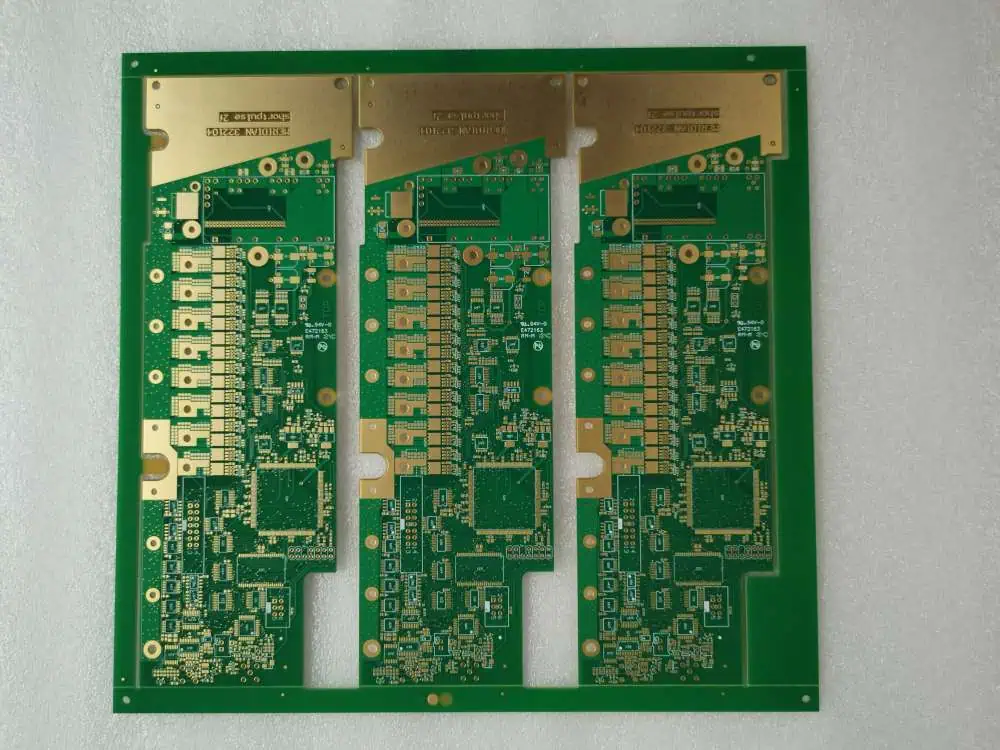
4.8mm 20 Layer PCB Manufacturing
RayMing is 20 layer PCB manufacturer ,Welcome to send your 20 layer PCB Design to sales@raypcb.com , We will give the best quote for you .
20-Layer PCB Stackup Selector 20LULTRA
Configure layer thicknesses for ultra-high-density 20-layer server, HPC, AI accelerator, datacenter switch, and advanced networking PCB designs
Quick Presets
Copper Layers (20)
Prepreg Layers (10)
Core Layers (9)
Stackup Visualization
3.5mm: Standard 20L
4.0-4.5mm: Server/HPC
5.0mm+: Backplane
Stripline: All inner SIG
Center: L10↔L11 tightly coupled
5 PWR: Multi-rail support
L10-L11: Ultra-low Z decoupling
5 GND Planes: L2, L6, L10, L13, L17 — Ground reference within 4 layers of every signal; L10 center GND provides symmetry axis and shielding.
5 PWR Planes: L4, L8, L11, L15, L19 — Support 6+ voltage rails with splits (VCore, VIO, VDDA, VDDQ, VPP, VCCSA); L10-L11 form ultra-low-inductance decoupling pair.
Via Strategy: Requires sequential lamination with blind/buried vias and microvias (stacked or staggered); via aspect ratio typically 12:1 max.
Material: Consider low-loss materials (Megtron 6/7, Tachyon, I-Tera MT40) for high-speed lanes >25Gbps.
Symmetry: Structure symmetric about Core 5 center for optimal CTE matching, warpage control (<0.5%), and reliable BGA/LGA reflow.
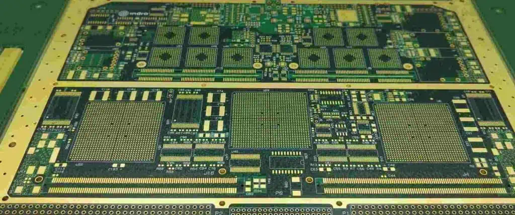
20 Layer PCB Stack Up


Introduction
20 layer PCBs enable remarkably dense and complex circuit designs for advanced applications. The multilayer board integrates signals, power distribution and components in a compact form factor. However, fabricating 20 layer boards reliably requires expertise in process control and testing. Selecting the right manufacturer is key to ensuring high yields and performance.
This article discusses capabilities required of a high quality 20 layer PCB production facility. We will go over recommendations for stringent process standards, precision equipment, rigorous testing and qualifications needed to deliver complex multilayer boards with high yields and low defects.
Key Capabilities for 20 Layer PCB Fabrication
Producing 20 layer PCBs pushes fabrication equipment and process limits. Here are some must-have capabilities:
- Handling board sizes exceeding 460mm x 610mm
- Stackup with 20 conductive copper layers interleaved with dielectric
- Tight layer to layer registration accuracy of ~50um
- Line width and spacing down to 3/3 mil with tolerances of +/- 0.5 mil
- Laser drilled and plated microvias with 5 mil diameter and pitch down to 8 mil
- 1 oz copper on outer layers, 0.5 oz for inner layers
- Various dielectric materials – FR4, Rogers, Polyimide, PTFE etc.
- Sequential lamination with advanced process controls
- Fine line imaging and etching on inner layers
- Excellent hole wall plating quality and copper bonding
- HDI technologies – microvias, stacked vias, blind/buried vias
- UL, ISO, and other certifications
Fabrication must also assure high yields across large board sizes typical for high layer count.
Critical Process Control Requirements
Achieving quality and repeatability involves refined process controls:
- Metrology tools to precisely monitor panel parameters in real-time
- Maintaining laminate and etchant integrity across long cycles
- Precise control of lamination temperature and pressure profiles
- Real-time drilling parameter adjustment – speed, depth, pressure
- High uniformity copper plating across panel with minimum voids
- Imaging, etching, stripping processes tuned for high yields
- Statistical feedback loops for continuous tolerance improvements
Refined process tuning, monitoring and control minimizes scrap and rework even when producing complex stackups.
Advanced Fabrication Equipment Essential
latest equipment allows holding the tight tolerances needed:
- Direct imaging with 50um lines/spaces rather than using artwork films
- High accuracy layer-to-layer registration system for stacking and lamination
- Laser microvia drilling machines with ~5mil capability
- Advanced plating equipment for uniform copper filling of blind and buried vias
- Automatic optical inspection systems to detect defects during fabrication
- Advanced patterning machinery capable of fine features on inner layers
Investment into cutting-edge fabrication tools enables reliable volume production of dense HDI boards.
Comprehensive Testing Is A Must
With the high layer count and complexity, testing assumes even more critical importance:
- Automated optical inspection after major fabrication steps
- Netlist testing of bare panels for opens, shorts and impedance
- Test point integration to enable probing all layers for shorts
- Microsection analysis of layer alignment, lamination and plated holes
- Complete functional testing of populated boards
- In-circuit tests for assembled boards with boundary scan capability
Extensive testing at bare board, assembly and functional stages is essential to achieve final yield targets for 20 layer PCBs.
Qualifications and Certifications
Validated capabilities, quality management and consistency controls differentiate tier-one manufacturers:
- ISO 9001, ISO 14001 certified facilities
- IPC 6012 Class 3, IPC 6018 Class 3 qualifications
- ITAR registration support for defense products
- UL listing for safety compliance assurance
- RoHS, REACH, Conflict Minerals compliance
- Ongoing reliability and improvement testing
- Statistical process control monitoring
These qualifications provide confidence in their process capabilities and infrastructure.
Finding Reliable 20 Layer PCB Manufacturers
Here are helpful tips when selecting a 20 layer PCB production partner:
- Review online capabilities – specifically for 20+ layer expertise
- Validate certifications are current and relevant
- Ask for customer references with 20 layer boards made
- Check facilities, equipment investments
- Review sample quality and test data
- Have initial engineering discussion – DFM, DFT, capabilities
- Assess supply chain – inventory, sourcing for prompt delivery
- Consider locations near your team for operational agility
Taking the time for thorough due diligence during selection ensures you choose the right long-term fabrication partner.
Conclusion
With stringent process controls, advanced fabrication equipment and comprehensive testing, capable manufacturers can reliably produce high-density 20 layer PCBs. Validated infrastructure and certifications provide confidence to take on challenging multilayer builds. Partnering early in design with an experienced 20 layer PCB producer helps navigate design and process complexities for a successful outcome. As electronics innovation pushes further, these partnerships continue enabling intricate products integrating multilayer boards with refined manufacturing.
Frequently Asked Questions
Here are some common FAQs on 20 layer PCB manufacturing:
What are typical 20 layer board thicknesses?
A 20 layer board with standard dielectrics and 1 oz copper can end up around 0.260” (6.6 mm) thickness. Using thinner dielectrics and copper under 0.5 oz reduces thickness.
What line width/space is achievable on 20 layer boards?
Leading manufacturers can achieve 3/3mil line/space on external layers and 5/5mil for internal layers using direct imaging down to 50um resolution.
What materials are used in 20 layer PCB construction?
FR-4 is common for cost-effective boards. High frequency boards use RF materials like Rogers RO4350b or ceramic-filled PTFE. Flexible boards may use polyimide films.
What are the main difficulties in fabricating 20 layer boards?
Maintaining tight layer registration and plating quality through many lamination cycles. Also achieving fine features on inner layers and high yields across large board sizes.
How is component density achieved on 20 layer boards?
High component density is enabled by HDI technologies like microvias, blind/buried vias and thinner dielectrics for routing channels.