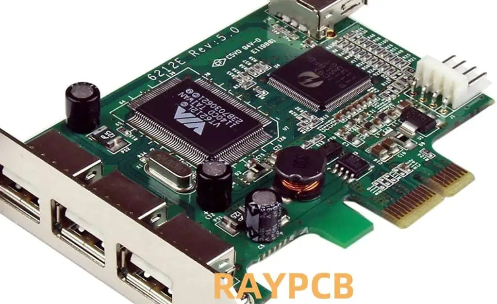
In the rapidly evolving landscape of cybersecurity, the demand for robust encryption solutions has never been higher. High-speed password cards based on the Peripheral Component Interconnect Express (PCIe) standard have emerged as a powerful tool in this domain. These cards offer unparalleled performance in encryption and decryption tasks, making them invaluable in sectors ranging from finance to government security. This article delves into the intricacies of PCB design and research for these cutting-edge devices, exploring the challenges, methodologies, and best practices in creating efficient and reliable high-speed password cards.

Understanding PCIe and High-Speed Password Cards
PCIe Technology Overview
PCIe (Peripheral Component Interconnect Express) is a high-speed serial computer expansion bus standard designed to replace older PCI, PCI-X, and AGP bus standards. It offers several advantages that make it ideal for high-performance applications like password cards:
| Feature | Benefit |
| High Bandwidth | Supports data transfer rates up to 64 GB/s (PCIe 5.0) |
| Low Latency | Minimal delay in data transmission |
| Hot-Pluggable | Allows for easy installation and removal |
| Scalability | Available in different lane configurations (x1, x4, x8, x16) |
High-Speed Password Cards
High-speed password cards are specialized hardware devices designed to perform encryption and decryption tasks at high speeds. They typically include:
- Dedicated encryption processors
- Secure key storage
- Hardware random number generators
- High-speed interfaces (e.g., PCIe)
These cards offload cryptographic operations from the main CPU, significantly improving system performance and security.
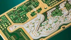
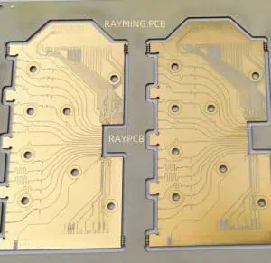
PCB Design Considerations for High-Speed Password Cards
Layer Stack-up and Material Selection
Layer Configuration
A typical high-speed PCB for password cards might use a 10-12 layer stack-up:
| Layer | Purpose |
| 1 | Signal (Top) |
| 2 | Ground |
| 3 | Power |
| 4.-7 | Signal |
| 8 | Power |
| 9 | Ground |
| 10 | Signal (Bottom) |
H3: Material Considerations
- Use low-loss materials like Megtron-6 or CLTE-XT
- Consider impedance control requirements
- Evaluate thermal management needs
Signal Integrity and EMI Considerations
Impedance Control
- Maintain consistent 100Ω differential impedance for PCIe lanes
- Use controlled impedance traces for high-speed signals
EMI Mitigation
- Implement proper grounding and shielding techniques
- Use stitching vias to reduce EMI
- Consider EMI suppression components like ferrite beads
Power Integrity and Distribution
- Implement robust power distribution network (PDN)
- Use decoupling capacitors to reduce power noise
- Consider using embedded capacitance layers for improved power integrity
Thermal Management
- Identify and address potential hotspots
- Implement thermal vias under high-power components
- Consider using heat sinks or thermal pads for critical components
Key Components and Their Layout
PCIe Controller
- Place the PCIe controller close to the edge connector
- Minimize the length of PCIe lanes
- Implement proper termination for signal integrity
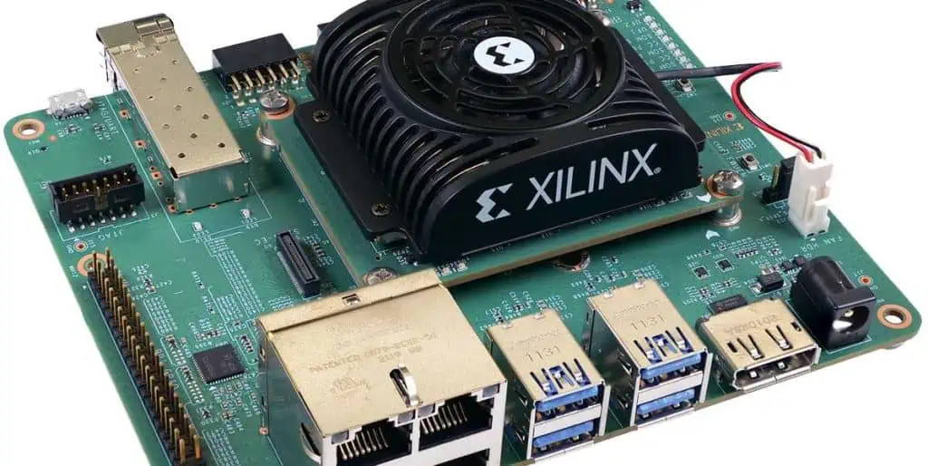
Encryption Processor
- Position the encryption processor centrally for efficient routing
- Ensure adequate power and ground connections
- Implement proper thermal management
Memory Components
- Use DDR4 or HBM2 for high-speed operations
- Implement proper fly-by topology for clock and control signals
- Adhere to memory manufacturer’s layout guidelines
Clock Distribution
- Implement a low-jitter clock distribution network
- Use controlled impedance traces for clock signals
- Consider using clock buffers for fan-out
High-Speed Signal Routing Techniques
Differential Pair Routing
- Maintain consistent spacing between differential pairs
- Use symmetrical routing for length matching
- Avoid sharp bends (use 45-degree angles or arcs)
Length Matching and Timing Considerations
- Implement intra-pair and inter-pair length matching for PCIe lanes
- Consider using serpentine routing for length matching
- Use timing analysis tools to verify signal integrity
Via Design and Transitions
- Minimize the use of vias in high-speed paths
- Use back-drilling to reduce via stub effects
- Implement proper via stitching for signal integrity and EMI reduction
PCB Fabrication and Assembly Challenges
High-Density Interconnect (HDI) Techniques
- Use microvias for high-density routing
- Implement stacked and staggered via structures
- Consider using laser-drilled vias for precision
Component Placement and Thermal Considerations
- Optimize component placement for signal integrity and thermal management
- Use thermal modeling to identify and address hotspots
- Consider using vapor chambers or heat pipes for advanced cooling
Testing and Verification
- Implement proper test points for in-circuit testing
- Use boundary scan (JTAG) for improved testability
- Consider using embedded test structures for signal integrity verification
Performance Optimization Techniques

Parallel Processing Architecture
- Implement multiple encryption cores for parallel processing
- Use efficient load balancing algorithms
- Optimize data flow between components
Memory Hierarchy and Caching
- Implement multi-level cache architecture
- Use high-bandwidth memory interfaces
- Optimize memory access patterns for encryption algorithms
Hardware Acceleration of Cryptographic Functions
- Implement dedicated hardware for common cryptographic operations (e.g., AES, SHA)
- Use FPGA-based reconfigurable logic for algorithm flexibility
- Optimize critical path delays in encryption circuits
Security Features and Considerations
Secure Key Management
- Implement a hardware security module (HSM) for key storage
- Use tamper-resistant packaging
- Implement key zeroization mechanisms
Side-Channel Attack Mitigation
- Implement power analysis countermeasures
- Use constant-time algorithm implementations
- Consider electromagnetic shielding
Secure Boot and Firmware Update Mechanisms
- Implement secure boot using hardware root of trust
- Use cryptographic signatures for firmware validation
- Implement secure firmware update mechanisms
Compliance and Certification
PCIe Compliance Testing
- Adhere to PCI-SIG compliance test specifications
- Perform electrical and protocol compliance testing
- Consider using compliance test boards for validation
FIPS 140-2/3 Certification
- Design with FIPS 140-2/3 requirements in mind
- Implement required cryptographic boundaries
- Document design and security features for certification process
EMC and Safety Certifications
- Design for EMC compliance (FCC, CE)
- Implement proper ESD protection measures
- Consider safety requirements for different markets (UL, TÜV)
Future Trends and Research Directions
Integration of Quantum-Resistant Algorithms
- Research implementation of post-quantum cryptographic algorithms
- Optimize hardware for lattice-based and multivariate cryptography
- Consider flexibility for future algorithm updates
Advanced Interconnect Technologies
- Explore optical interconnects for increased bandwidth
- Research advanced packaging technologies (2.5D, 3D IC)
- Investigate new materials for improved signal integrity and thermal management
AI-Assisted Cryptography and Design Optimization
- Explore AI-based attack detection and prevention
- Implement machine learning for dynamic algorithm selection
- Use AI-assisted tools for PCB layout optimization
Case Studies
High-Performance Enterprise Security Solution
- Design goals: 100 Gbps throughput, FIPS 140-2 Level 3 compliance
- Challenges: Thermal management, signal integrity at high speeds
- Solutions: Advanced cooling system, optimized PCIe Gen 4 implementation
Government-Grade Encryption Card
- Design goals: Multi-algorithm support, tamper-resistant design
- Challenges: Side-channel attack prevention, secure key management
- Solutions: Faraday cage implementation, dedicated HSM integration
Frequently Asked Questions (FAQ)
- Q: What are the key advantages of using PCIe for high-speed password cards? A: PCIe offers several advantages for high-speed password cards, including high bandwidth (up to 64 GB/s with PCIe 5.0), low latency, hot-plug capability, and scalability. These features allow for rapid data transfer between the card and the host system, enabling high-speed encryption and decryption operations. The PCIe interface also provides flexibility in terms of form factor and power delivery, making it suitable for a wide range of applications.
- Q: How does the PCB design for a high-speed password card differ from a standard PCB design? A: PCB design for high-speed password cards requires special considerations due to the high-frequency signals and security requirements. Key differences include:
- More complex layer stack-up to manage signal integrity and power distribution
- Use of specialized low-loss materials for high-speed signal propagation
- Stricter impedance control and signal routing techniques
- Enhanced thermal management to handle heat from high-performance components
- Implementation of security features like tamper-resistant designs and secure key storage
- Compliance with stringent EMI/EMC requirements due to high-speed operations
- Q: What are the main challenges in designing a PCIe-based high-speed password card? A: The main challenges include:
- Maintaining signal integrity at high speeds (10-16 GT/s for PCIe 3.0-4.0)
- Managing power integrity and thermal issues with high-performance components
- Implementing robust security features to protect sensitive data and keys
- Achieving compliance with various standards (PCIe, FIPS 140-2/3, EMC)
- Balancing performance, security, and cost in the design
- Ensuring reliability and longevity of the card in various operating environments
- Q: How is security implemented at the hardware level in these password cards? A: Security is implemented at the hardware level through several measures:
- Dedicated hardware security modules (HSMs) for secure key storage and management
- Tamper-resistant packaging and sensors to detect physical intrusion attempts
- Hardware-based random number generators for strong cryptographic operations
- Secure boot mechanisms using a hardware root of trust
- Isolated cryptographic boundaries to prevent unauthorized access
- Implementation of side-channel attack countermeasures (e.g., power analysis resistance)
- Hardware-accelerated encryption engines for secure and fast cryptographic operations
- Q: What future developments can we expect in high-speed password card technology? A: Future developments in high-speed password card technology may include:
- Integration of quantum-resistant cryptographic algorithms to prepare for post-quantum threats
- Adoption of advanced interconnect technologies like optical interconnects for even higher bandwidth
- Increased use of AI and machine learning for adaptive security and performance optimization
- Implementation of more advanced packaging technologies (e.g., 2.5D, 3D IC) for improved performance and reduced form factor
- Enhanced integration with cloud and edge computing infrastructures for distributed security solutions
- Development of more energy-efficient designs to meet growing sustainability requirements
- Increased focus on multi-tenancy and virtualization support for cloud and data center applications