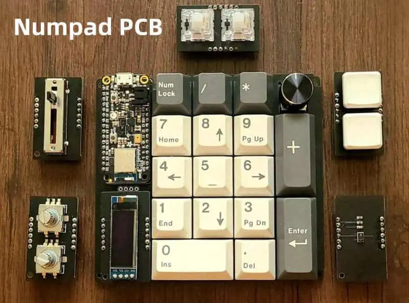
A numpad PCB refers to the printed circuit board used in numeric keypads typically located on the right side of computer keyboards. Numpads contain numeric keys, arithmetic operators, navigation buttons enabling efficient data entry especially for numerical information.
This article provides an overview of numpad PCB design considerations across architecture, layout factors, component selection and firmware functionality shaping end user experience. We also look at trends in custom wireless numpads.
Keypad PCB Architecture
The numpad PCB interfaces with the main keyboard matrix through data communication protocols like I2C or SPI to transmit key press information. Some variants implement USB connectivity requiring embedded microcontrollers.
Here is a typical numpad PCB architecture:
Key Components
- Key Switch Matrix – Scanned rows/columns to determine pressed key
- MCU – Handles switch matrix scan, lighting control and external interfaces
- Connectors – Link to main keyboard matrix or USB ports
- Lighting – LEDs for illumination and aesthetics
Below is a summary of common numpad connectivity approaches:
| Integration | Description | Complexity |
|---|---|---|
| Matrix Interface | Direct connection to keyboard matrix through I2C/SPI | Low |
| USB Device Wired | MCU enumerates as USB device with host | Medium |
| Bluetooth Wireless | Embedded BT SoC for wireless link | High |
Architecture selection depends on factors like cost, PCB area, wireless usage environment and software complexity.
Numpad Switch Matrix
The matrix of switches forms the core user interface for numeric key entry in numpads. The two predominant switch matrix architectures include:
Row-Column Scanning – Row lines are driven, column sensors read to detect key press through scan algorithm. Suits medium size matrices.
Diode Isolation – Each key has dedicated diode allowing continuous scans to find pressed keys. Higher reliability for large matrices.
The numpads use compact form factor switches like MX, Choc low profile and electrostatic E-dome switches occupying smaller PCB footprint. Typical electrical rating is 3V, 5mA. Some variants integrate 2 million operation lifespan rating.
For high reliability applications like POS terminals, metal dome or rubber cup switches provide IP65 sealing, vandal resistance and handle millions of keystrokes through long operational life.
Numpad Circuit Design
The numpad PCB circuit design involves:
Power Supply – Low noise 3.3V or 5V supply with adequate local bulk decoupling capacitors to filter noise on matrix sensing lines.
MCU – Microcontroller handles matrix key scanning through GPIO rows/columns, lighting LED PWM and communication to host through I2C, SPI or USB depending on connectivity option. Popular choices are ATmega328, STM32 and NXP LPC series MCUs offering robust USB libraries.
ESD Protection – MOV/TVS diodes should clamp any interface or ESD transients above USB/serial voltage specifications protecting internal MCU.
EMI Filters – Common mode chokes and filter ferrites minimize conductive and radiated interference meeting EMC compliance for certifications like FCC class B conducted emissions.
Indicator LEDs – Most numpads incorporate single color or full RGB LEDs under each translucent keycap for aesthetics and visibility in dark environments. MCU runs lighting patterns and effects through PWM output modules.
Numpad PCB Layout Considerations
Key numpad PCB layout considerations include:
- Match mechanical keepout area to intended keyboard enclosure
- Ensure switch footprint landing patterns accommodate chosen keycap stem style
- Place bypass capacitors adjacent to pins on MCU, Crystal and other ICs
- Routed controlled impedance tracks for USB D+/D- signals with length matching constraints
- Strategic group splits in ground plane under ICs with sensitive analog inputs pins
- Visual status indicator LEDs and current limiting series resistors positioned near keys
For numpads targeting compact low profile keyboards, PCB sizes range from 100 x 100 mm to 160 x 80mm rectangle formats. These integrate rigid-flex sections to fold and fit inside tight enclosures.
Wireless Numpad Implementation
Detachable wireless numpads using 2.4GHz RF, Bluetooth or Wi-Fi connectivity allow flexible positioning in work areas without cable constraints. They are powered using rechargeable batteries.
Here are some ways wireless is implemented:
Bluetooth SoC – Dedicated Bluetooth SoC/module handling host device pairing and wireless serial data with MCU to transmit keypress data. Allows low power sleep modes.
Multiprotocol Wireless MCU – Some STM32 and NXP LPC MCUs integrate wireless subsystem covering multiple protocols like Bluetooth 5.0, Bluetooth mesh, Thread, Zigbee allowing direct wireless connectivity and OTA firmware upgrades without external ICs.
Wi-Fi – ESP32 series wireless SoC integrates Wi-Fi/BT modem saving BOM over discrete solutions. downside is higher peak power consumption compared to BT only alternatives.
This is a functional block diagram of a wireless numpad PCB with charging/battery support:
Wireless solutions must address latency, reliability and seamless roaming between paired hosts for satisfactory user experience especially when moving across large workspaces.
Numpad Firmware Design
Firmware development is key to deliver optimized numpad functionality leveraging available hardware capabilities:
- Fast key scanning algorithm debouncing and accurately reporting multiple simultaneous key presses
- Advanced RGB lighting effects controlled through key press combinations
- Macro definition to output strings/patterns expanding single key usage
- Wireless security mechanisms like encryption, device whitelisting
- Low power modes with periodic wake eventing to maximize battery runtime
Combining compact PCB layouts with well-designed firmware allows creating unique numpads suited for niche applications.
Applications of Custom Numpads
Some common application areas where compact custom numpads deliver unique utility include:
Desktop Audio Controllers – Transport keys for playback control, scrolling jog wheels and slider potentiometers to adjust volume/bass/treble levels.
POS and Payment Terminals – Rugged numeric entry keypads for retail checkout counters, signature capture displays. Must meet security and certification requirements. Integrate NFC/swipe card readers.
Industrial Control Panels – Membrane sealed numeric keypads with E-stop switches for data entries and equipment state transitions. Handle harsh electrical noise.
Keyboard Macropads – Portable macro pads with OLED display allowing customization across productivity and creative applications through key sequences.
Gaming Keypads – Compact mechanical gaming keypads with premium switches aligned to meet needs of RTS/MOBA gaming genres.
FAQ
What switch options work with numpads?
Common switch options include compact MX mechanical switches, durable metal dome switches or ultra low profile butterfly mechanism switches depending on tactile needs, reliability requirements and enclosure depth constraints of target keyboard.
How does numpad interface with the keyboard?
Numpads generally interface to the keyboard controller through industry standard serial protocols like I2C or SPI to transmit key press data. Some models implement USB for direct host connectivity allowing greater placement flexibility.
What are numpad PCB sizes?
Compact numpad PCB sizes typically range from 100 x 100 mm up to 150 x 80 mm rectangular boards. Miniaturized layouts below 90 x 70mm are also feasible for highly space constrained wireless numpads using rigid-flex PCBs and choking EMI control components.
How is NFC integrated on numpads?
For applications like payment terminals, an NFC controller IC is added to the numpad PCB which operates in reader/writer mode interfacing with MCU UART/SPI to facilitate tap-based transactions through ISO/IEC 14443 Type A/Type B protocols modulation/encoding built into hardware.
What are use cases for custom numpads?
Some popular custom numpad applications are desktop media controllers with playback/volume keys, point-of-sale entry units for retail, industrial equipment data entry pads and macropads allowing extensive productivity software shortcuts. Compact numpad PCB foundation enables unique single hand data input devices.