What is a RoHS Compliant Lead-Free PCB Assembly?
RoHS compliant lead free printed circuit board (PCB) assembly refers to a circuit board assembly manufactured using lead free solder and components that comply with RoHS (Restriction of Hazardous Substances) standards and regulations.
RoHS is a European Union regulation that restricts the use of 6 hazardous substances in electrical and electronic equipment:
- Lead (Pb)
- Mercury (Hg)
- Cadmium (Cd)
- Hexavalent chromium (Cr6+)
- Polybrominated biphenyls (PBB)
- Polybrominated diphenyl ether (PBDE)
A lead free PCB assembly uses lead free solders such as tin-silver-copper (SAC) alloys rather than traditional tin-lead solder. Lead free PCB assemblies also use electronic components that meet RoHS requirements for maximum concentration values tolerated for the 6 restricted substances.
Benefits of Lead Free PCB Assembly
Some key benefits of using RoHS compliant lead free PCB assemblies include:
- Environmentally Friendly – Reduces hazardous e-waste and exposure of toxic substances to humans and the environment
- Regulatory Compliance – Meets RoHS and other global environmental regulation requirements for electronics
- High Reliability – Lead free solders can offer comparable or even better reliability than tin-lead
- Easier Recycling and Reuse – Due to lack of hazardous substances in assembly components
Many electronics manufacturers worldwide now require RoHS and lead free PCB board assembly for their products. Consumer demand for greener electronics is also driving adoption of lead free soldering process and components. For these reasons, PCB assembly service providers in China are moving towards sustainable manufacturing processes for global customers.
Why Choose China for Lead Free PCB Assembly?
China has emerged as the electronics and PCB manufacturing hub powering the world’s consumer electronics industry. Here are some of the key benefits of lead free PCB assembly services in China:
1. Cost Savings
China provides very competitive pricing for RoHS compliant and lead free PCB assemblies for export markets while still delivering quality. Manufacturing and labor costs are lower.
2. Production Capacity
High volume SMT assembly lines optimized for efficiency and scale. Able to handle fluctuating customer demand and production ramps.
3. Specialized Knowledge and Equipment
Chinese EMS companies continuously invest in the people, equipment, technology needed to assemble lead free PCBs, meeting latest quality and RoHS standards.
4. Supply Chain Advantage
Easy access to abundant Component sources and suppliers in China to mitigate electronic component shortages and lead times for customers globally.
With both capabilities and capacity for cost effective and compliant lead-free PCB assembly, China has become the go-to manufacturing base servicing a large percentage of global electronics OEMs including many American and European brands.
Key Parts in a Lead Free PCB Assembly
A lead free PCB assembly has three key components:
1. Lead Free Printed Circuit Board (PCB)
This refers to the bare PCB fabrication made of laminates, copper traces, and components pads/footprints using RoHS compliant materials and processes. Common substrates used are FR-4 and CEM-3.
2. Lead Free Components
This includes active and passive surface mount device (SMD) components used on the PCB that meet RoHS maximum concentration values tolerated for the six restricted substances according to IEC 62321 standard.
Some examples:
- Integrated circuits (ICs)
- Semiconductors
- Resistors, capacitors
- Transistors, diodes
- LEDs, relays
- Connectors
3. Lead-Free Solder
Lead-free solders replace conventional tin/lead solder to make solder connections between pads on the PCB and component termination finishes.
Common lead-free solder alloys used:
- Tin Silver Copper (SAC) alloy: SnAgCu
- Tin Copper (SACX): SnCu
Below is a breakdown comparison between conventional tin/lead solder characteristics versus lead-free SAC solder alloy commonly used:
| Characteristic | Tin/Lead Solder | Lead Free SAC Solder Alloy |
|---|---|---|
| Melting Point | 183°C | 217°C to 220°C |
| Wettability | Good | Moderate to good |
| Solderability | Good | Good |
| Electrical Conductivity | Excellent | Good |
| Mechanical Properties | Good | Good |
| Creep Resistance | Fair | Excellent |
| Fatigue Life | Good | Good |
| Thermal Cycling | Good | Good |
As the comparison table shows, the lead free SAC solder alloy offers comparable and even better performance than conventional tin/lead solder in some characteristics such as creep resistance while maintaining complete RoHS compliance.
Manufacturing Process for Lead-Free PCB Assembly
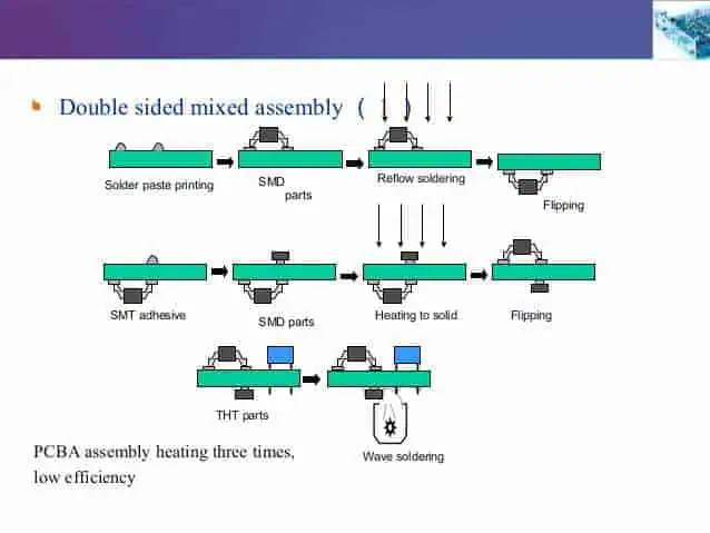
The basic manufacturing workflow to assemble RoHS compliant lead free PCBs involves two main processes:
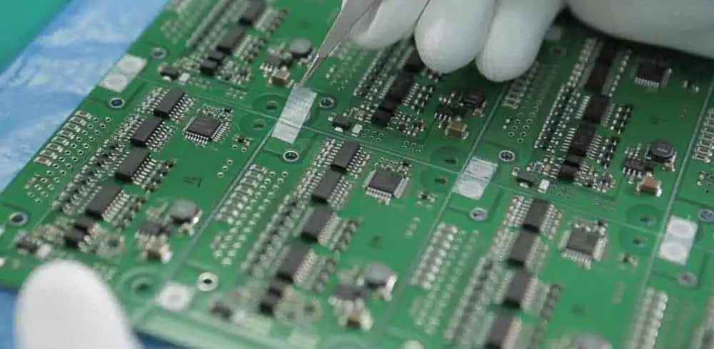
1. SMT (Surface Mount Technology) Assembly
This is assembly of surface mount device (SMD) components onto the PCB using lead free soldering techniques. The key steps are:
- Solder Paste Screen Printing – Lead free solder paste stencil is used to apply precise amounts of solder paste onto PCB pads
- SMD Component Placement – Use of high speed Pick and Place machines to accurately place tiny chip components onto PCB pads
- Solder Reflow – SMD components attached by passing PCB loaded with components through a reflow oven heating to melt solder paste and forming solder joints
2. Wave Soldering or Manual Soldering (for Through Hole components if any)
This second stage is for attachment of any leaded through hole (TH) components by:
- Wave Soldering – Passing the PCB bottom side through a molten lead free solder wave to solder leads into plated through holes.
- Manual Soldering – specialist operators use lead free solder wire and iron to hand solder leads
These two core assembly processes with RoHS compliant materials, when executed with extreme precision using well-tuned assembly lines, modern equipment, and strict process controls allows the manufacturer to deliver high yielding and reliable lead-free circuit board assemblies cost effectively in China.
Below illustrates a simplified sequence for manufacturing RoHS compliant and lead free PCB assemblies in China:
Quality Control and Assurance such as visual inspection, AOI, x-Ray, ICT testing is interwoven between manufacturing processes to verify assembly quality against defects.
Guide to Cost Factors for Lead Free PCB Assembly in China
What are the key cost drivers when estimating and comparing lead free PCB assembly quotes between Chinese electronic manufacturers? Below is an overview:
a) PCB Parameters
- PCB Class – Class 2, Class 3 PCB or higher have more layer counts impacting complexity
- PCB Size
- Copper thickness – 1 oz., 2 oz. or thicker copper PCBs
- Gold finger connectors – Expensive material addition
- V-cuts or special routing – Add additional fabrication costs
- Panel utilization – Batch PCB quantity being assembled for optimal efficiency
- PCB quantities and potential volumes
b) Component Parameter
- SMD component sizes – 0201, 0603, 1206 etc. The smaller, the harder and costlier it is to handle and assemble
- SMD component counts – total number of placements
- Complexity of bill of materials (BOMs) – total number of component/item line items
- High pin count SMDs – can be challenging to solder or re-work
- Number of BGAs or other special package components requiring x-ray inspection
- Total component placement value
- Component lead time and inventory overhead – for hard-to-source parts
c) Other Materials
- Solder paste – Some special solder wire or solder paste adds cost
- Adhesives or encapsulation epoxy – for protecting certain components
d) Secondary Operations
Secondary PCB assembly operations that could impact cost:
- Cleaning
- Conformal coating
- Programming or loading firmware/software
- Testing requirements and coverage beyond standard practice
- Box build with enclosure/cables
- Custom labeling, logo printing
e) Service Factors
Service parameters that add a premium:
- Low or fluctuating volume – increases down-time and changeover costs
- Expedited or “jump the queue” lead times below capability
- Documentation overhead – more process control plans required
- Extra production monitoring required – live video feeds
- High mix, slow ramp BOM and engineering change management
- Excess handling due to fragile boards or packaging requirements
By accurately accounting for above factors that incur additional material, process, quality or service costs, the manufacturer can provide realistic assembly pricing. Lead-free assembly in China balancing performance, quality, and fair cost then becomes very achievable.
FAQ – Lead Free PCB Assembly in China

Below are answers to some frequently asked questions foreign OEM customers have regarding outsourcing RoHS compliant and lead free electronics manufacturing to Chinese EMS suppliers.
Can you ensure RoHS compliance for PCB assembly in China? How?
Yes, any established mid to large size PCB assembly house in China supplying to export markets can guarantee RoHS compliance today. Here is why and how they achieve this:
1) Updated Equipment and Solder
They invest in new soldering systems, storage and handling that can enable lead-free manufacturing separating from tin/lead solder equipment.
2) Material and Component Controls
Strict receiving inspection and test procedures ensure only RoHS certified materials and pre-approved electronic components are used in production meeting IEC 62321max concentration requirements.
3) Process Controls and Operator Training
Soldering process window adjustments to account for higher melting point temperatures. Training on handling and storage of lead free solder paste and materials.
4) Compliance Verification
XRF material chemistry analysis and IPC testing validates RoHS thresholds ensuring no cross-contamination through adequate flushing during product transitions.
Taken together, these hardware, process, people and compliance measures ensure PCB deliverables comply with RoHS and other environmental directives for global customers.
Are there any reliability issues with lead free solder joint integrity? How is this addressed?
Lead free solder alloys in particular SAC 305 used today have well established excellent thermal cycling reliability comparable to tin/lead joints for standard PCB assembly.
However, for high reliability or thermal sensitive applications, there may still remain certain concerns to address:
- SAC Solder Joint Brittleness Use of SAC305 with addition of alloying elements like Ni, Bi, In, and Ce can enhance ductility, fracture resistance and anti-cracking capabilities.
- Intermetallic Compound (IMC) Formation
Optimizing reflow profile peak temperatures between 240°C to 260°C and minimizing time above 217°C can help restrict excessive IMC growth maintaining a strong but thin enough Cu-Sn IMC interface. - Mechanical Drop Shock or Vibration Resistance
Corner bonding and filleting performance tweaks during reflow process allows lead free solder joints better withstand drop test stresses. Underfill dispensing also helps strengthen mechanical integrity.
With experience addressing these and accounting for coefficient of thermal expansion (CTE) mismatches between PCB substrate material and mounted components using modeling analysis, the EMS provider can deliver robust lead-free assemblies passing reliability qualifications, even for automotive, aerospace, defence or medical application use under harsh operating environments.
How much more does lead-free PCB assembly cost in China?
In the past, RoHS compliant and lead free PCB assemblies used to cost anywhere from 5% to 15% higher for the exact same bill of materials (BOMs) and PCB as compared to tin/lead solder assembly. However, with almost all PCB assembly in China being completely lead-free for export regulated customers over the past decade, these initial cost premiums have reduced significantly. Most mature factories in China price and quote lead-free and leaded assembly identically now, with few exceptions for specialty applications requiring extra process steps to ensure solder joint reliability. Volume is really the biggest cost driver. So for mass produced consumer electronics and LED lighting PCB assemblies regularly manufactured in China, there should be minimal cost difference observed based simply on solder alloy used or availability of RoHS process certification.
What should I request from the factory to prove RoHS compliance?
To validate RoHS compliance and lead-free assurance from the Chinese PCB assembly factory before you award volume manufacturing business, be sure to request and review:
- RoHS certification – Such as ISO 9001 plus IEC QC 080000 certification audit report proving RoHS materials control and validated test reports for substances present below max concentration values.
- IPC Validation – Evidence of process capabilities meeting acceptability of electronic assemblies to IPC-A-610 Class 2 and J-STD-001 Class 2 criteria would indicate well-tuned RoHS capable assembly lines.
- XRF Material Chemistry Analysis Report – Sample XRF scan report needs to measure solder and part metallurgies verifying lead free material chemistry confirming no cross contamination for a recently assembled pilot build board randomly tested by laboratory.
The above documents should sufficiently address RoHS compliance validation and risk mitigation for your custom lead-free electronic or PCB product manufactured in China.
What lead time can be expected for prototype builds before mass production?
If most raw PCB fabrication materials and standard electronic components required for assembling the first prototype pilot run are available in China, customers can typically expect a 2 to 3 week turnaround time from Gerber design files approved to DHL express delivery of fully functional, lead-free assembled samples from China EMS partner.
Accelerating this lead time further is also possible by negotiation, typically by paying extra fees to either jump in the production queue ahead of other customers or else pay premium expedite fees to material suppliersViews and increase stock buffers for just your BOM requirement ahead of provisioning production. If exotic electronic components in BOM need imported procurement from overseas franchised sources, lead time gets pegged to longest component lead time. So procured component availability primarily governs overall prototyping board to mass production ramp up timescales.
What are some alternatives to lead free SAC solder alloy used by Chinese factories?
While tin/silver/copper (SAC) alloys like SAC305 or SAC405 formulated with 3 to 4% silver are the predominant lead free solder used for PCB assembly in China due to good wetting capability, suitable melting point and joint strength, some potential alternatives also being offered include:
- Low/No Silver Solders – Reducing precious metal like silver additions using formulas like Sn/Cu or Sn/Ag/Cu with 0.1% to 1% silver can lower material costs 20%-30%
- Bismuth Containing Solders – Alloys containing bismuth like Sn/Bi/Ag added provide enhanced ductility, thermal cycling fatigue resistance and drop test reliability
- Zinc Containing Solders– Small zinc alloying addition improves solder joint drop/shock integrity meeting IEC Drop Test requirements
So alternatives do exist to standard SAC305 lead free solderPaste (RoHS) used that provides either economic advantage or added board level reliability robustness where application use case warrants slight tweaks to material science formulation. Discuss options with your Chinese PCB assembly services provider.
I hope this comprehensive guide has addressed most aspects regarding outsourcing your RoHS compliant and lead free electronics manufacturing needs to China – from understanding associated costs to validating quality, compliance assurance, and timescales expectations when leveraging these globally accessible PCB assembly capabilities for your next turn-key products launch. Please free feel to contact me for any further questions!