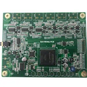
Design for Manufacturing and Assembly (DFMA) represents a critical methodology in modern electronics development, particularly for printed circuit boards (PCBs). This systematic approach integrates manufacturing and assembly considerations directly into the design phase, fundamentally transforming how engineers approach PCB development. By incorporating DFMA procedures early in the design process, organizations can achieve significant improvements in product quality, cost efficiency, and time-to-market while reducing manufacturing defects and assembly complications.

Understanding DFMA in the PCB Context
DFMA combines two complementary methodologies: Design for Manufacturing (DFM) and Design for Assembly (DFA). In PCB applications, DFM focuses on optimizing the board’s physical design to streamline fabrication processes, while DFA emphasizes simplifying component placement and assembly procedures. This dual approach addresses the entire production lifecycle, from raw material processing through final product assembly and testing.
The complexity of modern PCBs, with their increasingly dense component layouts, multilayer structures, and miniaturized form factors, makes DFMA procedures essential rather than optional. Today’s electronics demand high-density interconnects, fine-pitch components, and sophisticated routing architectures that push manufacturing capabilities to their limits. Without proper DFMA implementation, these advanced designs can result in prohibitively expensive manufacturing processes, unacceptable yield rates, and extended development timelines.
Cost Optimization Through Strategic Design Decisions
One of the most compelling arguments for implementing DFMA procedures lies in their profound impact on manufacturing costs. Studies consistently demonstrate that design decisions made during the initial phases of product development influence 70-80% of total manufacturing costs. By applying DFMA principles, engineers can identify and eliminate cost drivers before they become embedded in the final design.
Component selection represents a primary area where DFMA procedures deliver substantial cost benefits. Rather than choosing components based solely on electrical performance specifications, DFMA-guided selection considers factors such as component availability, standardization opportunities, and assembly complexity. This approach often reveals that slightly different components with similar electrical characteristics can dramatically reduce manufacturing costs through improved automation compatibility or reduced handling requirements.
Manufacturing process optimization through DFMA extends beyond component selection to encompass board design decisions that directly impact fabrication costs. Layer count optimization, via size and spacing specifications, drill hole sizing, and material selection all significantly influence manufacturing expenses. DFMA procedures provide structured frameworks for evaluating these trade-offs, enabling designers to make informed decisions that balance performance requirements with cost constraints.
Quality Enhancement and Defect Reduction

DFMA procedures serve as powerful quality enhancement tools by systematically identifying and eliminating design features that contribute to manufacturing defects. Many common PCB quality issues, including solder joint failures, component misalignment, and thermal stress problems, originate from design decisions that inadequately consider manufacturing realities.
Solder joint reliability, a critical factor in PCB longevity, benefits significantly from DFMA-guided pad design optimization. Proper pad sizing, shape selection, and thermal relief implementation can dramatically improve solder joint formation and long-term reliability. DFMA procedures provide guidelines for optimizing these parameters based on component types, assembly processes, and operational requirements.
Component placement optimization through DFMA procedures addresses another major source of quality issues. By considering factors such as thermal interactions, mechanical stress distributions, and assembly sequence requirements, designers can create layouts that minimize component stress and improve overall reliability. This systematic approach often reveals placement conflicts that might otherwise remain undetected until prototype testing or production phases.
Manufacturing Process Compatibility and Efficiency
Modern PCB manufacturing involves numerous specialized processes, each with specific requirements and limitations. DFMA procedures ensure that design decisions align with these manufacturing capabilities, preventing costly redesigns and production delays. This compatibility extends across the entire manufacturing chain, from board fabrication through component placement, soldering, and final testing.
Assembly process optimization represents a particularly important aspect of DFMA implementation. Automated assembly equipment, including pick-and-place machines and wave soldering systems, operates most efficiently when PCB designs accommodate their specific capabilities and limitations. DFMA procedures provide structured approaches for optimizing component orientations, placement sequences, and assembly accessibility to maximize automation efficiency.
Testability considerations within DFMA frameworks ensure that completed assemblies can be efficiently verified and debugged. This includes providing adequate test point access, minimizing test fixture complexity, and incorporating design features that facilitate automated testing procedures. These considerations, when implemented early in the design process, can significantly reduce testing costs and improve production throughput.
Risk Mitigation and Design Robustness
DFMA procedures function as comprehensive risk management tools by identifying potential manufacturing and assembly challenges before they impact production schedules or product quality. This proactive approach enables design teams to address issues during the development phase when modifications are relatively inexpensive and schedule impacts are minimal.
Supply chain risk mitigation represents an increasingly important aspect of DFMA implementation. By considering component availability, alternate sourcing options, and end-of-life considerations during the design phase, engineers can create more resilient designs that maintain manufacturability despite supply chain disruptions. This strategic approach has proven particularly valuable in recent years as global supply chain challenges have impacted electronics manufacturing worldwide.
Design robustness improvements through DFMA extend beyond component selection to encompass layout optimization for manufacturing variations. Real-world manufacturing processes involve inherent variability in component placement accuracy, solder paste deposition, and thermal profiles. DFMA procedures help designers create layouts that maintain functionality despite these normal manufacturing variations, resulting in higher yield rates and more consistent product performance.
Implementation Strategies and Best Practices
Successful DFMA implementation requires systematic integration into existing design workflows rather than treatment as an afterthought or checklist exercise. This integration typically begins with establishing clear design rules and guidelines that reflect both manufacturing capabilities and cost targets. These rules should be regularly updated to reflect evolving manufacturing technologies and capability improvements.
Cross-functional collaboration represents a critical success factor for DFMA implementation. Effective programs involve manufacturing engineers, assembly technicians, quality personnel, and procurement specialists in the design review process. This collaborative approach ensures that all relevant manufacturing perspectives are considered and that design decisions reflect comprehensive understanding of production requirements.
Design review procedures should incorporate formal DFMA evaluation criteria alongside traditional electrical and mechanical verification processes. These reviews should occur at multiple project phases, allowing for iterative optimization as designs evolve and requirements become more clearly defined. Early-phase reviews focus on architectural decisions and component selection strategies, while later reviews address detailed layout optimization and assembly sequence planning.
Future Considerations and Emerging Technologies
As PCB technologies continue evolving toward higher densities, faster signal speeds, and more complex integration requirements, DFMA procedures must adapt to address new manufacturing challenges. Emerging technologies such as embedded components, flexible-rigid constructions, and advanced packaging techniques introduce new variables that must be incorporated into DFMA frameworks.
Artificial intelligence and machine learning technologies are beginning to enhance DFMA implementation by automating routine design optimization tasks and identifying optimization opportunities that might be overlooked by manual analysis. These tools can process vast amounts of manufacturing data to identify patterns and correlations that inform design decisions and improve manufacturing predictability.
The increasing emphasis on sustainability and environmental responsibility is also influencing DFMA procedures, with growing focus on material selection, end-of-life considerations, and manufacturing process environmental impacts. Future DFMA implementations will likely incorporate comprehensive lifecycle assessment criteria alongside traditional cost and quality metrics.
Conclusion
DFMA procedures represent essential methodologies for modern PCB development, delivering measurable improvements in cost efficiency, product quality, manufacturing reliability, and time-to-market performance. Their systematic approach to integrating manufacturing considerations into design decisions helps organizations navigate the increasing complexity of modern electronics while maintaining competitive advantages in rapidly evolving markets.
The investment in comprehensive DFMA implementation pays dividends throughout the product lifecycle, from reduced development costs and shorter design cycles through improved manufacturing yields and enhanced product reliability. As PCB technologies continue advancing and manufacturing requirements become increasingly sophisticated, organizations that embrace DFMA principles will be better positioned to succeed in competitive electronics markets while delivering superior products to their customers.