High Density Interconnect (HDI) technology has revolutionized the design and manufacturing of large, dense printed circuit boards (PCBs), enabling unprecedented levels of miniaturization and performance in modern electronic devices. As component densities continue to increase and form factors shrink, HDI layer stackup design becomes critical for achieving optimal electrical performance, manufacturing reliability, and cost-effectiveness in complex electronic systems.
Understanding HDI Technology Fundamentals
HDI PCBs are characterized by their use of microvias, buried vias, and sequential build-up layers that allow for significantly higher routing density compared to traditional PCB designs. The defining feature of HDI boards is the microvia structure, typically with diameters of 150 micrometers or less, which enables fine-pitch component placement and high-density routing. These microvias are formed through laser drilling, allowing for precise hole formation that would be impossible with mechanical drilling techniques.
The sequential lamination process used in HDI manufacturing allows for the creation of complex layer stackups with multiple build-up layers on each side of a core substrate. This approach enables designers to route high pin-count components like ball grid arrays (BGAs) and chip-scale packages (CSPs) while maintaining signal integrity and minimizing board real estate requirements.
Strategic Stackup Planning for Large Dense PCBs
When designing HDI stackups for large, dense PCBs, several fundamental principles must guide the planning process. The stackup must accommodate high-speed digital signals, power distribution requirements, thermal management considerations, and manufacturing constraints while maintaining mechanical stability across large board dimensions.
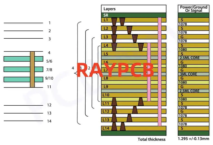
Layer count determination begins with component pin-out analysis and routing density calculations. Large dense PCBs often require 12 to 20+ layers to accommodate complex routing requirements. The distribution of these layers between signal, power, and ground planes requires careful optimization to ensure adequate power delivery, signal isolation, and electromagnetic compatibility.
Power distribution network (PDN) design becomes particularly challenging in large HDI boards due to increased power consumption and the need for multiple voltage rails. The stackup must incorporate sufficient power and ground planes positioned strategically to minimize impedance and provide adequate decoupling. Typically, this involves dedicating 30-40% of the layer count to power distribution, with careful attention to plane pairing and via transitions.
Signal Integrity Considerations in HDI Stackups
High-speed signal routing in large dense HDI PCBs requires meticulous attention to controlled impedance design and crosstalk mitigation. The stackup must provide consistent impedance profiles across all signal layers while accommodating various signal types including single-ended, differential pairs, and high-speed serial interfaces.
Dielectric selection plays a crucial role in achieving target impedance values while maintaining low loss characteristics for high-frequency signals. Modern HDI designs often employ low-loss dielectric materials with stable dielectric constants across temperature and frequency ranges. The choice between different prepreg and core materials must balance electrical performance with manufacturing feasibility and cost considerations.
Via transitions present unique challenges in HDI designs, particularly when signals must traverse multiple build-up layers. The stackup design must minimize via stub lengths through the use of back-drilling or blind/buried via structures. Sequential via transitions, where signals move from one build-up layer to another through carefully planned via chains, require precise impedance modeling to prevent signal degradation.
Thermal Management Integration
Large dense PCBs generate significant heat that must be efficiently dissipated to maintain component reliability and performance. The HDI stackup design must incorporate thermal management features including thermal vias, heat spreading planes, and strategic copper balancing to facilitate heat transfer from high-power components to heat sinks or thermal interfaces.
Thermal via design in HDI stackups requires careful coordination with the electrical routing to avoid interference while maximizing thermal conductivity. Dense arrays of small thermal vias often prove more effective than larger, less numerous vias for heat transfer from surface-mounted components to internal ground planes or dedicated thermal layers.
Copper balancing becomes critical in large HDI boards to prevent warpage during manufacturing and operation. The stackup must maintain relatively uniform copper distribution across layers while accommodating varying routing densities in different board regions. This often requires the addition of copper fills, hatching patterns, or dummy features in lightly routed areas.
Manufacturing Constraints and Design Rules
HDI manufacturing imposes specific constraints that must be considered during stackup design. Sequential lamination processes require careful attention to registration tolerances, especially in large boards where thermal expansion can cause significant dimensional variations. The stackup design must accommodate these manufacturing realities through appropriate design margins and tolerance allocations.
Microvia formation through laser drilling requires specific material combinations and thickness limitations. Each build-up layer must conform to manufacturer capabilities regarding minimum via sizes, aspect ratios, and capture pad dimensions. These constraints often influence layer thickness selection and routing strategies throughout the stackup.
Aspect ratio management becomes particularly important in thick HDI stackups. While mechanical drilling can achieve higher aspect ratios for through-hole vias, the combination of through-holes and microvias in a single stackup requires careful optimization to ensure reliable via formation and plating. This often necessitates the use of staggered via structures or multiple via transitions to connect signals across the full board thickness.
Advanced HDI Architectures
Modern large dense PCBs often employ advanced HDI architectures including any-layer HDI (ALDI) and embedded component technologies. ALDI allows via formation between any two layers in the stackup, providing maximum routing flexibility but requiring sophisticated manufacturing processes and design verification.
Embedded passive components, including resistors and capacitors built directly into the PCB substrate, can be integrated into HDI stackups to further increase functional density. This approach requires specialized materials and manufacturing processes but can significantly reduce component count and improve electrical performance through reduced parasitic effects.
Package substrate integration represents another advanced approach where the PCB stackup is designed to accommodate flip-chip mounting of bare die or advanced packaging technologies. This requires extremely fine feature sizes and specialized materials but enables unprecedented integration levels for high-performance applications.
Design Verification and Testing Strategies

Large dense HDI PCBs require comprehensive design verification including electromagnetic simulation, thermal analysis, and mechanical stress evaluation. The complex stackup structures and high component densities make traditional design rule checking insufficient for ensuring reliable operation.
Signal integrity simulation must account for the complex via transitions, layer changes, and coupling effects present in HDI stackups. Three-dimensional electromagnetic modeling becomes essential for accurate prediction of high-frequency behavior and optimization of critical signal paths.
Power integrity analysis must verify adequate power delivery across all voltage rails while accounting for the distributed nature of power distribution in large boards. This includes evaluation of voltage ripple, transient response, and electromagnetic interference from power distribution networks.
Manufacturing design for testability becomes challenging in dense HDI designs due to limited test point accessibility and high routing density. The stackup design must incorporate provisions for in-circuit testing, boundary scan testing, and functional verification while maintaining signal integrity and routing efficiency.
Cost Optimization Strategies
HDI manufacturing costs scale significantly with layer count, via complexity, and feature density. Effective stackup design must balance performance requirements with cost constraints through strategic material selection, via optimization, and manufacturing process selection.
Selective HDI implementation, where high-density features are used only in areas requiring maximum routing density, can provide cost savings while maintaining overall board functionality. This approach requires careful interface design between HDI and conventional PCB sections but can significantly reduce manufacturing complexity and cost.
The future of HDI layer stackup design for large dense PCBs continues to evolve with advancing materials technology, manufacturing capabilities, and electronic system requirements. Success in this field requires careful integration of electrical, thermal, mechanical, and manufacturing considerations to achieve optimal performance, reliability, and cost-effectiveness in increasingly complex electronic systems.