Which Amplifier is Used to Provide Increased Bandwidth?

broadband amplifier

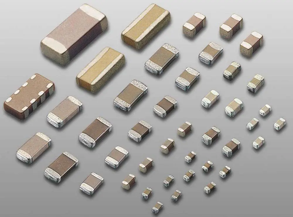
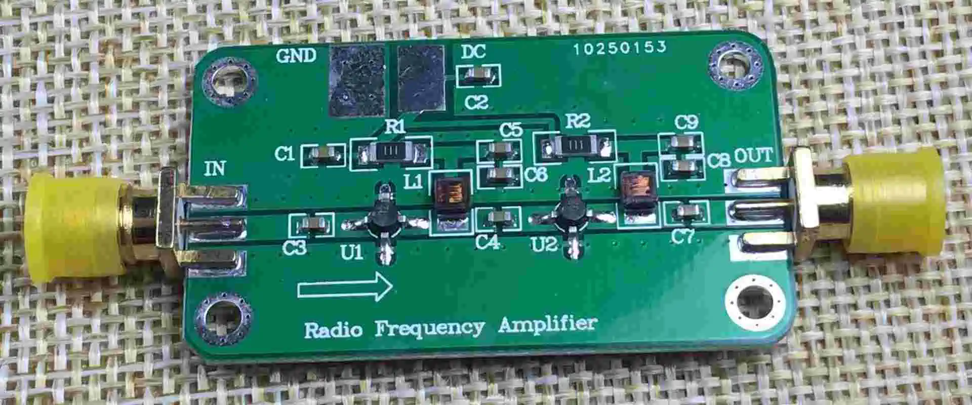
A broadband amplifier is an electronic device that can handle high-frequency signals. The output power of such an amplifier is usually much higher than its input power. The input voltage of a broadband amplifier can be as low as 50 mV rms but can easily exceed 140 mV pk-pk. This circuit features a current-feedback amplifier, a common design choice for a broadband amplifier.

There are three basic types of broadband amplifiers. There are untuned amplifiers and tuned amplifiers. Both types of amplifiers use an inductor and a capacitor. A tuned circuit has a peak response at a certain frequency, but it also displays gain for a band around that frequency. We measure the bandwidth of a broadband amplifier from the -3 dB down points in the frequency range.

Is Broadband a Microwave Amp?

broadband amplifier design

A broadband power amplifier is a critical component of wireless communications systems and applications. This comprehensive resource combines theory and practice for efficient design and development. It will appeal to both practitioners and students alike.

Broadband microwave amplifiers fall into two categories: klystron and cross-field. The former is based on transistor technology, while the latter is a multi-stage device focusing on signal efficiency and noise reduction. As a result, broadband microwave amplifiers can boost microwave equipment’s efficiency by up to 70%.

Broadband microwave power amplifiers provide high power, low noise, and a broad linear amplification range. They are available in both solid-state and traveling wave tube designs.

A broadband amplifier is difficult to design at higher power levels. Since the product of bandwidth and power is for the particular amplifying device, obtaining such a wide bandwidth is difficult.

As a result, microwave power amplifiers use various techniques to achieve their desired power levels. The two approaches depend on theoretical analysis and circuit simulation. A broadband amplifier is also widely used in communication systems.

What Device Can Amplify an output Signal?

An amplifier is a device that uses an external power source to amplify a signal. There are several types of amplifiers, including Class-D amplifiers and Operational amplifiers. All types require an external power source to operate. These devices are also called transducers.

Transducer

A transducer is a device that transforms energy from one form to another. When you receive a signal in one form, the transducer will change the energy into the other form. It is an essential part of any device that sends and receives signals. It can be helpful in a variety of applications, including medical applications.

There are several kinds of transducers. For example, one type of transducer can measure temperature. Another type can measure depth. The type of input that a transducer can determine its sensitivity.

A transducer consists of two elements – detecting and transduction elements. The sensing element responds to environmental changes by generating an output, such as a voltage, angular displacement, or strain. The transducing element acts on this response to produce an output proportional to the sensing element’s change.

Amplifier modules on the power supply

Amplifiers increase the power and gain of an electrical signal. They’re essential components of stereos, radios, and television sets. They’re also helpful in wireless communications and broadcasting. Here’s how they work.

An amplifier uses multiple stages to boost the signal. A transistor-based amplifier, for example, boosts the signal many times before it reaches a tiny loudspeaker in the ear canal.

An amplifier works by receiving an input signal from a source, such as a turntable or CD player. It then enlarges that signal by passing it through a series of components. It also receives power from a 110-volt wall socket. An amplifier has three main connections. You can connect your music player, a DVD player, and a power supply.

An amplifier’s voltage gain describes how much it amplifies a signal. We often measure it in decibels (dB). For example, good rf amplifiers -3dB bandwidth will be between 20 Hz and 20 000 Hz, where human hearing occurs. Another essential property of an amplifier is its dynamic range, which is the range between its highest and lowest output amplitude without output noise power.

Class-D amplifier

FULL PCB MANUFACTURING Quote

A Class-D amplifier is an electrical amplifier that operates on the principle of pulse width modulation. Its switching frequency is high, typically 300kHz, or 15 times the highest audio frequency of general interest.

The higher the switching frequency, the higher the resolution and signal-to-noise ratio. However, a high switching frequency also reduces the efficiency of the amplifier.

A Class-D amplifier’s main causes of nonlinearity are dead-time and switching timing errors. Nonlinearity in a Class-D stage is due to dead-time, which can reach 1% of total harmonic distortion.

The key to reducing this effect is to ensure accurate switching timing. A Class-D amplifier’s output stage has three distinct operation regions, each following different edges of the high-side input signal.

A Class-D amplifier can be more efficient than a Class-A/B amplifier. This is because the transistors are switched instantly and at near zero power. However, the switching process generates high-frequency noise power, which we must filter. The signal quality of the low-pass filter will also affect the sound of the Class-D amplifier.

Operational amplifier

An operational amplifier is a device that converts an electrical signal from one form to another. It has two inputs and one output. An inverting input holds a signal at ground (0 V), while a non-inverting input holds a voltage at its maximum value, either positive or negative. The device’s output depends on the input type and its negative feedback resistor.

The frequency response of most operational amplifiers is simple and linear, with the voltage gain constant at DC and very low frequencies. As a result, a single-pole roll-off occurs at approximately 6 dB/octave, or – 20 dB/decade.

We call this the gain-bandwidth product, indicating how well an operational amplifier offers excellent performance at high frequencies. Moreover, most operational amplifiers continue to have a single-pole response after gaining unity.

Operational amplifiers are sensitive to the input impedance. However, in a perfect world, the output impedance of an operational amplifier is zero. This is because the input voltage of an operational amplifier cannot be higher than its output impedance.

However, real rf amplifiers always have some variation, called the Common Mode Rejection Ratio (CMRR).

Which Amplifier is Used to Provide Increased Bandwidth and output power?

An amplifier provides increased bandwidth. The Doherty amplifier is one such type. These amplifiers have relatively low output impedances. This means that they are very effective at providing bandwidth enhancement. They are also very versatile and are often helpful in various applications. However, deciding which type is right for your application can be difficult.

Doherty amplifier

A conventional Doherty amplifier only increases bandwidth when the carrier and peaking cell impedances are different. A relatively low current generally characterizes peaking cells. An asymmetrical Doherty PA avoids this problem by applying more power to the peaking cell. An asymmetrical Doherty PA also allows load modulation, which can be an advantage.

A conventional Doherty amplifier consists of a quarter-wave input impedance transformer and an output combiner. Its efficiency is about 31% for power levels backed off six or seven dB from saturated output power. However, we can improve efficiency by incorporating a dual-bias circuit structure.

Another way to improve the efficiency of a Doherty amplifier is to use a dual-input digitally-driven design. This design can improve the performance of Doherty transmitters. Its adaptive phase-alignment mechanism minimizes power loss, increasing total output power. Furthermore, the relative improvement in output power was greatest in medium input drive levels.

Subcircuits

A preferred embodiment of a circuit has two or more non-linear subcircuits, each of which applies a specific transfer function to a certain range of an input gain. Outside of the range, the output of each sub-circuit is constant.

Additionally, the circuit can include a linear transfer performance, whose output cancels out the gain of the other sub-circuits.

An additional type of feedback circuit is a voltage-follower stage. A voltage-follower stage monitors and transmits the gain that flows into the transistor’s collector. This circuit becomes part of the feedback network, which complicates analysis. For example, a circuit uses two resistors to form a gain divider.

The value of C1 can give the desired fall-off in gain at the low end of the bandwidth. This is because inductive reactance, which increases with frequency, reduces the gain of a high-frequency amplifier. This effect is known as stray capacitance.

Voltage follower

Taconic RF-35A2 Ultra pcb

The voltage follower amplifier is a summing amplifier in which the output gain follows the voltage. It amplifiers are typically non-inverting devices that use a constant source as an input. As a result, their output impedance is low, and they are ideal for circuit isolation.

Voltage follower amplifiers have a low output resistance, which is very close to zero. Their output resistance depends on the type of op-amp used. In the case of a high-power gain follower, the output resistance is typically much lower than the resistance. However, they also can provide high output current.

A voltage follower amplifier is also known as a unity-gain amplifier. It works by increasing the current in a circuit without increasing the gain. Its output voltage follows the gain and is usually helpful in applications where the low gain from the source is beneficial. Its low-impedance design allows it to function without external components that would increase the output impedance.

Regenerative amplifier

Regenerative amplifiers are efficient, high-speed amplifiers. They can generate various pulse widths, including femtosecond and near-femtosecond pulses. In addition, they can produce longer pulses than standard amplifiers.

To achieve this, a regenerative amplifier must be oriented so that the effective bandpass is at 850 nm. Then, we inject seed laser pulses into the resonant cavity of the amplifier. T

his process amplifies the laser pulses through multiple traversals of the cavity. The seed laser pulse is then recompression to the desired pulse width.

A broadband regenerative amplifier is a critical component in a high-power laser facility. It smooths the spectrum by introducing spectral dispersion and phase modulation into the front-end seed source. It can effectively suppress FM-to-AM conversion.

Choosing a Coaxial Cable for Low Noise Amplification

When choosing a coaxial cable for low noise amplification, there are many things to consider. There are multiple factors to consider, including ground loops, double shields, impedance, and capacitance. A well-designed coaxial cable can reduce noise figure and provide a stable signal. Listed below are some features to consider. The higher these attributes are, the better. For example, double shields will reduce ground loops in addition to high impedance and low capacitance.

Double shields

Double shields in the coaxial cable can reduce the noise generated by the signal. They consist of various materials, depending on the type of connection. For example, some have spiral shields wound around the dielectric, while others consist of braided wires. Some also have a combination of braid and foil shields.

In a low noise amplification system, a double shield can increase the signal-to-noise ratio of a signal. This is because the shield is connected to the enclosed circuit ground at one point and is capable of coupling noise figure into the signal line. In addition, a double shield can provide additional shielding, as the outer shield can be connected to the rest of the shielding while the inner shield connects to the source ground inside.

High impedance

Low noise amplification requires cables with low noise characteristics. You must handle these cables with more care than ordinary cables. They should not be crimped, kinked, or stretched. In addition, they should never be run over or stepped on.

Even though the characteristic impedance of the cable is a critical factor in low noise amplification, it is not always possible to obtain a perfect match. This is particularly difficult if the source impedance is very low. A matched source and cable will increase the power transfer. A common base and gate topology may be required, while a common collector or drain topology is helpful with a medium source impedance.

A good rule of thumb for choosing a low noise figure cable is to choose a cable with an impedance less than the system’s total impedance. For example, a 10kO pot has a maximum length of four meters, while a coax with a high shunt capacity should be even shorter.

Small capacitance

A small capacitance coaxial cable is an essential component in low noise amplification. The total resonance capacitance is the sum of the cable capacitance and the tuning capacitance Cp. These are the same amount but different. The difference is in the expression of the noise figure.

A small capacitance coaxial cable is the best choice for low noise amplification. The cable has two conductors and insulating material in between. As a result, its capacitance is low, typically measured in picofarads. You can determine the exact amount by multiplying the capacitance value by the cable length. This will determine the level of the signal transmitted.

Ground loops

A ground loop is a kind of interference that can affect a signal’s transmission quality. We create it when a long cable connects to two devices. These devices have the same signal impedance, but the signal line connects to different grounds. This could be the shield of coaxial cable or the safety grounds of power supplies. In either case, the large loop picks noise gain near an interference source. This interferer degrades the signal seen by Device #2, which hinders transmission.

Nonlinearity

We can exploit coaxial cable’s inherent nonlinearity to create high-quality, low-noise amplification. The inductance of the center conductor causes nonlinearity. However, this inductance has enough strength to create a parametric solid amplification.

The loss of a coaxial cable is 3.2 dB at 1 GHz and five dB at GPS frequencies. LNA offsets this loss, which adds gain to the low-power signal. In addition, the LNA is used in signal chains to boost signal power from frequency generators and local oscillators.

The Y-factor method can measure the noise temperature. The Y-factor method also measures noise temperature in a mil-likelvin environment. However, this method requires custom components and is not widely available. In addition, the differences between the temperature points may result in systematic errors.

Summary of Broadband Amplifiers

Broadband amplifiers are devices that boost the frequency range of audio signals. They have two types: untuned and tuned. Untuned amplifiers have a single fixed peak response at a particular frequency, and tuned circuits have a variable peak response over a wider frequency range. Tuned amplifiers use an inductor and capacitor to determine the frequency range they can amplify.

Broadband amplifiers are used in various situations and can improve sound quality, reduce interference, and extend range and pitch. For example, analog signals are prone to interference, manifesting as fading, garbled sound, or static.

Higher-frequency digital transmissions also suffer from interference. Broadband amplifiers increase range by increasing the power at which sound waves can travel.

Broadband amplifiers typically employ a current-feedback amplifier as the main component. Other amplifiers have a wide bandwidth and are ideal for transmitting RF signals.

In addition, it is possible to eliminate some redundant hardware, such as a quarter-wavelength transformer, by modifying the Doherty topology.

Benefits, features, and application of a Microstrip antenna

Microstrip antenna

Microstrip is a planar transmission line made of a dielectric layer, similar to a coplanar waveguide. It was developed in the 1960s by ITT Federal Telecommunications Laboratories in Nutley, New Jersey, as a rival to stripline.

We can do early work with this type of transmission line using fat substrates, which allows non-TEM waves to propagate, making the results unpredictable. However, the device became very popular after the development of thinner microstrips.

A microstrip patch antenna radiates electromagnetic waves because of its fringing fields surrounding its surface. As a result, it has a low current value at the feed end and a large one at the center of the half-wave patch. This low current value accounts for the high impedance at the feed end.

To understand why this type of transmission line is called a microstrip, it is essential to understand the antenna theory. Microstrips are thin and flexible, unlike traditional transmission lines, meaning we can cut them into virtually any shape or size. This makes them the perfect solution for various applications, including RF circuits.

A microstrip line is not immersed in one dielectric material but is dielectric on both sides, which increases the characteristic impedance as the frequency increases. This property allows microstrip lines to work at very low frequencies and higher frequencies. However, this technique is limited to a few GHz due to losses.

The Most Common Printed patch Antenna

Microstrip antennas are commonly helpful in wireless communication systems. A microstrip antenna is a rectangular array with a length L that is one-third to one-half wavelength long.

They have a relatively low dielectric constant (typically 2.0 to 10.0), which results in greater efficiency. One crucial factor to consider when designing a microstrip antenna is the height of the substrate, as this directly affects efficiency and bandwidth.

A microstrip antenna consists of a metal patch connected to a dielectric substrate on one side. The patch is excited by an electrical current flowing across the dielectric substrate’s bottom ground plane.

The resulting antenna produces maximum radiation along the broadside and nearly zero radiation along the edge. The design process for a microstrip antenna often requires numerical methods to model its structure. The work of Pozar and Schawbert led to the development of sophisticated designs.

Microstrip antennas can be classified into several types but are the most popular. They play an important role in wireless communications systems due to their lightweight and thin profile. Another benefit of patch antennas is that they are easy to manufacture and are compatible with integrated circuitry.

Patch antennas are widely helpful in wireless communication systems. This is because they are easy to design and manufacture. They are also extremely inexpensive and a popular choice for various wireless applications. A rectangular microstrip antenna consists of a dielectric substrate with a metal patch on one side.

Microstrip patch Antenna benefits

A microstrip antenna is a versatile, low-cost antenna that can be manufactured easily and produces high-quality signals. Its benefits include low manufacturing cost, lightweight, and directivity. Read on to learn more about this popular antenna. You may be surprised by how many uses it has!

Low cost

Patch antennas are highly versatile and low-cost to manufacture. They are low in weight, small in size, and offer low radiation power. They can operate in dual and triple frequencies and are suited for various applications.

The low-profile design of these antennas makes them easy to incorporate into a circuit board. They are also easy to mount on a rigid surface.

Microstrip antennas are typically very thin. Therefore, we often print them on a single dielectric substrate or separately. Microstrips are a low-cost antenna design because they have no moving parts. Patch antennas consist of a layer of dielectric material. Each layer consists of 60 RF MEMS varactor elements.

Easy to manufacture

Microstrip antennas are a simple and inexpensive design that is very flexible. The planar structure allows them to conform to surfaces without losing their mechanical strength, even when mounted on rigid materials.

These antennas are helpful in many applications, and their low profile makes them easy to integrate into a device. They are also inexpensive to produce and can print onto a circuit board.

The microstrip antenna can consist of many different materials. A common material is an aluminum, which is incredibly easy to work with. We can cut and form the metal in a simple machine. The aluminum microstrip is easy to assemble, and the aluminum substrate makes it lightweight and durable.

Lightweight

Microstrip patch are low-profile, lightweight antennas that operate at a wide frequency range. In addition, they are easy to manufacture and integrate. These characteristics make them attractive candidates for use in wireless communication systems.

This paper explores various design issues related to microstrip antennas’ performance, such as gain enhancement, bandwidth, and reconfigurability. It also highlights a few examples of applications that benefit from this technology.

Patch antennas are available in a variety of shapes. The most common shape is a patch antenna, which uses a series of strips in an array. Some common shapes include a square, a circular ring, or an elliptical shape. Patch antennas are low-profile and lightweight, making them ideal for applications where space is limited.

Directivity

The directivity of a rectangular microstrip antenna is its ability to capture electromagnetic energy. We can manipulate them by changing the patch size and using an appropriate matching network. For example, a rectangular patch antenna with a width of 0.5 cm can have a gain of 0.7 dB.

Directivity is a function of the dielectric constant and the permittivity of the patch. An antenna with a larger dielectric constant has higher directivity than one with a smaller one.

Patch antennas radiate because they have a very advantageous voltage distribution. This makes them current radiators. By comparison, a wire antenna radiates because the currents add up in phase

Small distances

Patch antennas have two parts: a conductive strip and a dielectric substrate. This method is helpful for short distances, where we fabricate high-frequency signals without sacrificing efficiency.

However, it is not essential for use over a long distance. In addition, the antennas’ narrow bandwidth makes them unsuitable for use in large area networks.

Patch antennas are a relatively modern invention. They enable the integration of antenna and driving circuitry on a single circuit board or semiconductor chip.

This enables high dimensional accuracy, which was previously impossible with traditional fabrication methods. A microstrip antenna’s geometry consists of a thin dielectric substrate with a metal patch on one side.

Types of Microstrip Antennas

Custom antenna PCB
Custom antenna PCB

Microstrip patch consist of several types of materials. The conducting patch can be FR-4, RT-Duroid, foam, Nylon fabric, etc. They can also consist of dielectric substrates with different dielectric constants. The dielectric substrate is helpful for fabrication, and it is usually thick. Each type uses a different feeding technique to feed the patch to the substrate.

Parasitic patch

A parasitic patch antenna is a stacked microstrip antenna with a radiating part composed of nine rectangular metal patches arranged in three rows and three columns. Because of this regular concept makes the antenna’s radiation pattern uniform and can cover a wide bandwidth.

The antenna has a central patch 24 that couples to several smaller patches, or “parasitic patches,” which couple to each other at the center frequency f. The central patch 24 contains a slot 40 and two equal-sized notches, 44 a and b, each 125 mm wide.

As the spacing between the parasitic patches increased, so did the antenna’s profile. In addition, the antenna’s resonances shifted to lower frequencies. As a result, input impedance, reactance and resistance also decreased as the Hf increased.

Dielectric chip

The dielectric loading in a microstrip antenna profoundly affects the radiation pattern and impedance bandwidth. The higher the dielectric constant, the smaller the bandwidth of the antenna. In addition, increasing the substrate’s relative permittivity increases the antenna’s Q factor.

This is why the radiation pattern of a rectangular microstrip antenna is an array of slots. The highest directivity occurs when the dielectric of the substrate is air. Therefore, the relative permittivity of the dielectric increases as the substrate becomes more dielectric.

Antennas with high efficiency and high bandwidth have the advantage of being small and lightweight. However, there are several disadvantages to using a thin dielectric. Firstly, the ground plane significantly affects a microstrip antenna’s radiation resistance. Secondly, a microstrip antenna’s efficiency is negatively affected by the size of the dielectric.

A microstrip patch antenna is widely helpful in wireless communication systems. They are easy to make, and we can produce them in various shapes. The most common type is a patch antenna, but other microstrip patch use the patch as a constitutive element.

Patch

Microstrip antenna patch design can be challenging, especially if you need to increase bandwidth and cross-polarization. Fortunately, there are solutions. One of the easiest methods is to increase the height of the substrate. This will result in a larger effective radiation height. Another way to increase the effective radiation height is to use multiple patches.

Microstrip antenna patch designs consist of a probe connected to the patch and the ground plane. This method allows for efficient feeding and minimizes spurious radiations.

Another method, called aperture coupled feeding, couples the patch antenna to the feeder through a slot in the ground plane. This technique minimizes the likelihood of interference and increases the antenna’s bandwidth.

Microstrip antenna patch designs are also easy to manufacture. These thin antennas are lightweight and compact and suitable for flexible mounting on flexible circuit boards. Microstrip antenna patch designs are widely helpful in mobile communication and other areas. These antennas are also useful for remote sensing and environmental instrumentation.

Microstrip

A microstrip antenna is a type of internal antenna. They are most helpful for microwave frequencies. They consist of thin strips of metal, and are useful in many applications. These strips consist of gold or silver. This type of antenna is also commonly helpful in microwave ovens. A microstrip antenna is beneficial in many applications where a longer, stronger antenna is needed.

The radiation of antenna elemets are a function of the fringinging field surrounding the antenna. A side view shows that the current is zero at the end of the patch and is maximum at the center of the half-wave patch. This explains why the antenna impedance is so high at the end.

Microstrip patch is inexpensive and easy to manufacture. Their size is directly related to the wavelength at the resonant frequency. Single patches typically provide 6-9 dBi of directive gain, but patch arrays are capable of higher gains. In addition, the patches we can print using lithographic techniques. This type of antenna is also helpful for phase adjustment and matching.

Microstrip Antenna features

microstrip antenna types

Microstrip antennas are two-dimensional physical geometries that are cheap to produce, and we can print on substrates. They are helpful in various applications, including GPS technology, mobile satellite communications, Direct Broadcast Satellite (DBS) systems, remote sensing, and more. In addition to these uses, a printed antenna are also helpful in non-satellite applications, including medical hyperthermia.

Low-profile

Low-profile microstrip transmission line is ideal for use in mobile satellite communications systems. These antennas are flexible enough to conform to land vehicle roofs or aircraft wings.

One such antenna is in U.S. Pat. No. 5,220,335 (Huang). It includes microstrip patch elements and is tilted 40 degrees from its normal direction. This antenna has a low profile and high radiation efficiency, which is necessary for efficient mobile communications.

The design must reduce the overall size of a microstrip antenna. This process involves several optimization stages. The first step is to analyze the geometry of a proposed microstrip antenna. Once the geometrical parameters are determined, the design process will begin. This process is called characterization.

This antenna is a low-profile, rectangular patch microstrip antenna that operates on two frequency bands at once. We can achieve the dual-band characteristic by adjusting the slot size and inset-feed point.

One then prints the designed antenna onto an FR4 substrate. Measurements indicate that the realized antenna works on dual bands with a bandwidth of 45 MHz and 95 MHz. It also achieved a gain of 4.08 dBi for 1.8 GHz and 5.79 dBi for 2.4 GHz.

A low-profile printed antenna is excellent for mounting on metallic objects. These antennas can be as small as 1.6 mm in thickness. They offer high gain and a low profile. They are suitable for many UHF radio frequency identification applications. One advantage of these antennas is their versatility and low cost

Low-profile microstrip antennas offer high performance and wide bandwidth. The proposed antenna has a TM10-mode co-excited, TM20-mode antiphase, and a well-matched slotline transition.

Wideband

Wideband microstrip antennas are reconfigurable antennas with adjustable bandwidth and frequency. They are widely helpful in commercial, industrial, and military applications. The current research focuses on reconfigurable antennas with wide bandwidth and flexible frequencies. The proposed antennas have numerous applications and can easily integrate into a wide range of wireless devices.

A wideband printed antenna comes in different shapes and modes. They can be circular, dipole, square, or rectangular. Each shape has different radiation properties. The dipole is convenient as it has favorable radiation characteristics and occupies less space. Single and multi-feed arrays are also available for this technology.

The dielectric constant of the substrate is closely related to the width and bandwidth of the antenna. Therefore, if the dielectric constant is low, the antenna will have higher bandwidth. On the other hand, if the dielectric constant is high, the antenna will be compact and smaller. Therefore, the dielectric constant is a critical parameter in designing a microstrip antenna.

A wideband microstrip antenna is an extension of the traditional microstrip antenna. Its frequency response is comparable to that of its matched-pattern counterparts. Input impedance bandwidth is twice that of a traditional microstrip antenna. Its resonant frequency range is 4.72 to 6.79 GHz.

Wideband microstrip antennas have a lower impedance bandwidth than monolithic antennas, but they can be helpful for wireless applications. The design of the wideband microstrip antenna is a combination of both.

Microstrip antennas can radiate frequencies ranging from 2.7 GHz to 9.5 GHz. Therefore, this antenna is widely helpful in wireless communications. Its design features a defected ground plane to improve the gain. The maximum gain of the wideband microstrip antenna is 34 dB at 3.55 GHz.

Inefficient

Microstrip antennas are often curved and triangular. These shapes provide better impedance matching. The properties of an efficient microstrip antenna depend on its size, which typically ranges from five to six dB. In addition, the antenna design depends on the resonance frequency and pattern required. Finally, we choose the slots to produce the necessary bandwidth and gain.

Inefficient antenna elements have several disadvantages. They have low efficiency, poor power, and poor polarization purity. They also have a limited frequency bandwidth. However, in some applications, they can replace horn antennas. In addition, we can make them in various shapes and sizes.

An efficient microstrip antenna is an essential component in next-generation wireless communication systems. Its use in 5G communication systems is necessary to meet the exponential growth in data traffic.

However, this technology demands antenna arrays that are low profile. Microstrip patch antennas are a viable option but still have several drawbacks, such as low directivity and substrate thickness.

We can explain the radiation characteristics of an inefficient microstrip antenna in terms of fringing fields. For example, when you look at a patch antenna in a side-on view, you can see that the current is zero at the end. This is because the current in the patch is maximum in the center of the half-wave patch. The low current value at the end of the patch explains the high impedance.

Graphene offers greater bandwidth than copper. Additionally, it has a reduced resistance. Graphene also reduces stub-matching problems. Graphene can also be helpful in ultra-wideband applications.

Design and Measurement of Microstrip Antenna

FULL PCB MANUFACTURING Quote

Microstrip antennas are widely helpful for mobile communication systems. They are thin-film structures characterized by a narrow bandwidth and a circular or rectangular shape.

The most common type of MSA is a rectangular structure without a ground plane or dielectric material. The rectangular structure has a single polarization with radiating edges at each end of the L-dimension. Therefore, the radiation at the W-dimension is much less, called cross-polarization.

EM waves radiate out on a ground plane

Microstrip antennas radiate electromagnetic waves by combining two or more parallel layers of material. Therefore, we can stack these strips to improve directivity and bandwidth. In addition, leaky waves can further increase the antenna’s directivity. These advantages make antenna elements a popular choice for wireless communications.

Microstrip antennas can radiate waves in many different wavelength ranges. This allows for the creation of a wide variety of wireless communications devices. These antennas can consist of metal, plastic, or even glass. Many of them also have high transmission efficiency and low insertion loss.

Microstrip antennas are generally rectangular. They are made of a high conductivity metal, usually copper. The metal patch sits on top of a dielectric substrate. The substrate thickness is not critical, but the height h must be smaller than the wavelength of operation. If the height is too small, the antenna will not radiate efficiently.

EM waves contribute to the radiation pattern

The contribution of EM waves shapes the radiation pattern of a Microstrip antenna. Several factors contribute to this radiation pattern. One of these factors is substrate thickness. An antenna with a thin dielectric substrate has a lower effective radiation height than one with a thick substrate.

A parasitic patch is an additional element that can increase the radiation height. We can optimize the antenna’s effective radiation height by adjusting the size of the parasitic patch. One often prints them on a dielectric substrate with a foam layer on top of it.

A microstrip antenna array is very simple and inexpensive. Their main advantages include their high-frequency sensitivity, low-cost, low-profile, and lightweight design. They are also highly efficient and have high gains.

EM waves contribute to the impedance bandwidth

A microstrip antenna is a rectangular patch of metal that is excited by a voltage source across its bottom ground plane. It produces optimum radiation when excited in broadside directions and virtually zero radiation along the edges. A microstrip antenna can be modeled accurately by numerical methods. Pozar and Schawbert developed sophisticated designs for the microstrip antenna.

The microstrip antenna impedance bandwidth depends on the frequency of EM waves. For example, at 868 MHz, the antenna’s resonant frequency is too high. To minimize the frequency response, a discrete matching network may be helpful, which includes a 6.5-pF parallel capacitor and a 21.8-nH serial inductor.

Using software simulations to design a microstrip antenna array is essential for ensuring optimum performance. For example, using a simulation program like Sonnet, you can design matching networks to ensure that the antenna’s impedance bandwidth is optimized and that power transfer is near perfect.

EM waves contribute to the scan blindness

To minimize scan blindness, the antenna should reduce EM waves that propagate along its edges. However, conventional bandgap materials cannot eliminate the problem. Their radiating modes propagate in the substrate and couple elements, making them incapable of functioning as isolated radiating elements. To minimize scan blindness, the antenna should have modes that can suppress surface and substrate waves.

The scan blindness angle of a metal dielectric antenna depends on the substrate thickness and the permittivity. Using TSS, we can eliminate scan blindness in the H plane. The TSS acts as a hard surface in the H plane and guides the waves between the antenna elements.

In addition, the interelement spacing is uniform. Therefore, calculating scan blindness makes it possible to predict the antenna’s performance based on the propagation constants.

EM waves from microstrip antennas generate as they pass through the antenna. The dielectric under the patch causes polarisation currents, contributing to far-field coupling. The dielectric under the patch is also responsible for mutual coupling.

What Does Assembled PCB SMT Mean?

PCB prototype assembly suppliers

As the electronics design of today becomes more complex and smaller, more engineers have now decided to rely on SMT (surface mount technology). After 1980s, the assembled pcb smt technology was transformed into the most preferred technology for PCB assembly during electronics manufacturing. This hasnโ€™t been let up ever since.

The majority of the components of your phone might have been made through surface mount technology. Also, the majority of a carโ€™s components were most likely manufactured through assembled PCB smt.

Now the question is, what does assembled PCB smt mean, and why is it important for this technology to be created.

What is Assembled PCB SMT?

Assembled PCB smt is a way of producing electronic circuits. This is made possible by the placing of components on the surface of the board directly.

Assembled PCB smt is known as an option to the thru-hole or through-hole PCB manufacturing method. As manufacturing of electronics kept gaining momentum, a better and more efficient process now became important. This is how assembled PCB smt came to be. Assembled PCB smt comes with different uses. Also, it has some limitations that the design team must look into.

What are the Advantages of Assembled PCB SMT

Similar to the through hole type, assembled PCB SMT comes with some advantages and disadvantages. Letโ€™s consider the advantages of assembled PCB smt.

Affordable

The birth of the assembled PCB smt was mainly to reduce the costs of manufacturing. assembled PCB smt usually needs the drilling of fewer holes in your printed circuit board. This helps in lowering the handling and processing costs significantly

Lastly, the assembled PCB smt can produce high volumes. This allows a more preferable per-unit cost.

Efficiency

This is another significant benefit of the assembled PCB SMT. It makes use of the space of the circuit board more efficiently. As a result of assembled PCB SMT, engineers now have the ability to finagle different complex electronics in smaller assemblies.

Asides from its efficient use of the space present on the PCB, the process of SMT will be much faster. This will allow the manufacturer to increase the total output. This means that what would have taken about two hours to finish up using the through=hole technology, will only take ten to fifteen minute with the assembled PCB SMT.

Simplicity

For thru-hole assembly, the lead wires usually pass into the holes to help in connecting the components. Due to the fact that the soldering of the components are done onto the printed circuit board, the general makeup will be less complex.

Fewer Errors

The assembled PCB smt relies greatly on SMT machines. SMT is an almost totally automated process; this makes it less prone to any errors.

It can make use of smaller components

With assembled PCB smt, you will be able to make use of smaller, more compact, and lighter components than the through hole method

With this feature, engineers have been able to maximize the space on the printed circuit board, without having to compromise on the performance or function. Furthermore, manufacturers will be able to reduce the productsโ€™ weight. This makes them very portable.

The ability of making use of higher power components

The higher powered components are also useful in assembled PCB SMT rather than the through hole technology whereby the leads of the component are inserted in the holes that are drilled into the solder joints of the printed circuit board. Also, this will allow a higher density for packing and then gets rid of the importance of lead forming. This could be time consuming and difficult.

What Benefits Does it Bring to the assembled PCB SMT Process?

FULL PCB MANUFACTURING Quote

Helps in easing assembly

Due to the fact that component leads are usually surface mounted onto the pads, then lead forming isnโ€™t necessary. This ensures that SMT assembly comes faster and much simpler than the through hole technology. For the latter, the component leads have to be bent to form a specific shape and then inserted in holes that are drilled into the solder joints of the printed circuit board

Reliability

Typically the assembled PCB smt components are usually more reliable compared to the through hole types. This is because they are usually less prone to any shock and vibration. Furthermore, using solder paste rather than molten solder helps in reducing the component failure chances as a result og the cold solder joints

It can make use of fine pitch components

With assembled PCB smt, you can make use of very good pitch components. This isnโ€™t possible when using the thru-hole technology. Also, this advantage could be a major one for applications whereby there is limited space, as well as a high component density.

Versatility

Assembled PCB smt technology is very versatile. You can also use it for different applications. This include telecommunications, consumer electronics, industrial control system, and medical devices

Can make use of mixed technology printed circuit boards

Using the assembled PCB smt technology, it is possible to have printed circuit boards that combine both the surface mount and through hole components. This is very useful especially in applications where there are space constraints necessitating the use of the two connectors.

What are the Disadvantages of the assembled PCB smt Technology

Just like all the processes involved in manufacturing, assembled PCB smt come with some disadvantages.

One of the most important disadvantages is that it needs higher attention to every detail compared to the through hole assembly. Though the process is completely automated, the design parameters must be met so as to produce a reliable end product.

There can be an issue when the assembled PCB smt is used in placing the components onto the printed circuit board which will function in conditions involving:

  • Environmental stress
  • Mechanical stress
  • Temperature stress

You can mitigate this issue by blending the assembled PCB smt with the processes of the thru hole so as to enjoy the benefits of the two.

Conclusion

To summarize, assembled PCB smt is a way of producing electronic circuits. This is made possible by the placing of components on the surface of the board directly.

Humanoid Robots and the future of humans

Humanoid Robot

You may be asking yourself, “What is a humanoid robot?” Well, in a nutshell, a humanoid robot is a robot that has the form and function of a human. They talk, walk, and express a wide range of emotions. These robotic machines are very much like humans and could be the next step towards becoming fully human. Read on to learn more about humanoids and their role in our future.

Humanoids are machines that have the form or function of humans

These machines can perform tasks like humans, such as walking and talking. Many countries are deploying robots to relieve tired nurses in hospitals. Other uses of robots include basic cleaning and deliveries. Industrial robots can maintain production in manufacturing facilities. These machines can eventually replace humanoids.

While robots come in many shapes, the most endearing ones are those that look like people. Some examples of humanoid robots are Baymax from the Disney movie “Big Hero 6” and Transformers. These robots can emulate human characteristics, creating a lot of interest in the robotics industry. They can even serve the needs of physically disabled individuals. While these robots are still in development, they will eventually be a part of the daily lives of human workers.

They walk like humans

The first humanoid robot was Herbert Televox. Ron Wensley designed it at Westinghouse Electric and Manufacturing Co. Herbert Televox, the first robot innovation ambassador, could answer phone calls by lifting its receiver and control simple processes like operating switches based on signals. Though it was too slow to talk at first, it later evolved to say two simple sentences. However, despite the early success of the robot, it’s still not the perfect humanoid.

In early 2000, Japan was at the forefront of humanoid robot research. Kato’s WABOT-1 is one of the first academic humanoid robots. It can walk, recognize objects, and manipulate objects using hand movements. While walking, its movements are quasi-static and slow. In addition, it can maintain its total center of mass within a support polygon. Despite the early limitations, humanoid robots continue to be developed and willย revolutionize the world of robotics.

The Defense Advanced Research Projects Agency (DARPA) is working toward making a humanoid robot to carry out basic human tools and activities. The Asimo robot, developed by SRI and funded by DARPA, has a similar design, though its abilities are less impressive than those of the ATLAS robot. But while it is still a way off from being used in combat, humanoid robots can make our lives more convenient.

In a car factory, the Ford Motor Company has a humanoid robot that looks like a dog. These robots also have their names, Fluffy and Spot. Boston Dynamics, a subsidiary of SoftBank robotics,ย created them. Their main objective is to collect data for a detailed computer model of a manufacturing operation. Eventually, they will help carry out a variety of other jobs.

They talk like humans

AI algorithms are part of the software of Humanoid Robots. These algorithms are responsible for reasoning, learning, perception, and interaction. They use their internal workings to interoperate with humans and respond to their environment. The robots may soon be capable of interacting with human subjects. In the future, these robots will be capable of recognizing gestures and body posture and interpreting their intentions.

While a human can converse with a human-like robot, it’s not easy to communicate with a machine that doesn’t speak a native language. In addition, the physical texture and the first impressions of a human-like character play a role in our perception of a robot’s personality. For instance, trash talking in games has a long history of flustering game opponents. Robots can also be a source of discouragement – something humans can’t handle. However, researchers have designed a system to understand navigation apps and virtual assistants.

The Nadine robot is the world’s most humanoid robot. Its face and voice are accurate and realistic. The robot can identify people, shake hands, and carry on conversations based on previous meetings. Nanyang Technological University in Singapore developed its software platform. The robot citizen is essential as a customer-service agent for Kokoro, a Japanese company.

The technology behind these robotic humanoids is becoming more advanced. A new generation of humanoid robots will revolutionize the workplace. Humanoid robots will perform laborious, repetitive, and dangerous tasks that humans cannot.

They will replace humans for jobs that require constant and hazardous tasks. The most promising applications include a wide range of manufacturing, maintenance, and inspection tasks.

An advanced humanoid robot can express a wide range of emotions

The popularity of social robots continues to rise, and research into displayed emotions has increased over the last two decades. From 2000 to 2020, more than 1600 scientific publications exist in this field. Compared to the early 1990s, this rate has increased continuously.

An essential step toward developing humanoid robots is determining the sensitivity of the robots’ sensors to emotions. The following sections will explain how humanoid robots express different emotions and how they may be helpful in human-robot interactions.

The basic motivation behind emotion-generating robots is to mimic the natural behaviors of humans. People can express multiple emotions using facial expressions, gestures, and brain feedback. Therefore, human facial expressions, body movements, and speech are excellent data sources for this research.

These data can then help develop robots that exhibit human-like cognition and behavior. But this research isn’t limited to emotion-generating ubtech robotics. It also needs to account for the dynamic nature of emotions during HRI.

While humanoid robots can’t completely mimic human facial expressions, they are beginning to get there. One such humanoid robot, named Octavia, works in the Navy to fight fires. While the robot can mimic human faces, its facial expressions are impressive. Octavia resembles a human-size doll when it is off-duty. It has a white face, a snub nose, and eyebrows that sit evenly on the forehead.

Several studies have explored how human responses to robotic emotions influence the intensity and duration of the interaction. But, of course, whether humans can identify with a robot’s emotions largely depends on the context and people’s experiences.

Interestingly, however, the current state of research suggests some methodological and conceptual research recommendations that hold promise for generating meaningful impacts. And further empirical studies are needed to test whether these suggestions effectively predict human emotions.

A humanoid robot can be moral without sensations

Suppose we build a humanoid robot without sensations, but it still makes moral decisions. We might find this unsettling because we are used to the sensations that accompany a human’s moral decisions. What is the “something” that makes humans moral? It might not be sensations, but we do have moral cognitive faculties. Nevertheless, we don’t understand why we judge a moral decision of a humanoid robot differently from a human.

People don’t trust them for many reasons, including their incompetence. They think robots will fail in many human jobs, including nannies and nurses, firefighters, comedians, and others. But robots would be amazing package deliverers, receptionists, servers, and tour guides.

Researchers couldn’t determine where people got their biases, but they speculated that they might have picked up some bad press from stories about ubtech robotics falling into swimming pools. The researchers found that people’s biases toward robots could be related to a bias against women. In addition, they found that humanoid robots were trusted only when the jobs were straightforward.

While humanoid robots can be moral without feelings, the debate about whether such machines can be moral focuses on the robots’ effects. Popular discussions on the ethics of giving a feeling to robots often focus on the trauma imposed on them by humans. Films like Blade Runner and Westworld explore this dilemma by examining how the emotions of human-robot relationships may move to macco robotics.

While we have evolved over a long period to become ethical, the process of moral development is still far from complete. Unlike humans, macco robotics are not born ethical beings. Developing ethical robots requires a lot of research. For example, a humanoid robot with no sensations is unlikely to be ethical, but it may be possible.

How Far Away Are Humanoid Robots?

FULL PCB MANUFACTURING Quote

While some question how far humanoid robots can be, others have already created them. Some engineers have been struggling to break through the uncanny valley, a region of human-likeness where cute becomes creepy. Hong Kong-based Hanson Robotics is trying to avoid the creepy factor with its agility robotics.

Elon Musk’s Tesla Bot

The future of robotics is not far off. Elon Musk recently announced that his $1.1 billion factory in Austin, Texas, would be home to the Tesla Bot. It’s still a prototype and isn’t available yet, but the tech titan says it will be ready to roll out next year. Although the Tesla Bot is still a ways off, we can expect it to have many benefits for us in the future.

This isn’t the first time that Elon Musk has mentioned the creation of a robot. Last year, he announced that the robot would be the company’s most important project for the coming year. He even showed a human-like humanoid in a robotic suit dancing on stage, which has since become a meme. The Tesla Bot will likely use the same artificial-intelligence systems as Tesla vehicles, but there’s no way to tell just how far away it is until a prototype is ready.

The company’s CEO announced that the robot would be human-overpowered, but it still has a long way to go. The robot will weigh 125 pounds and stand five feet eight inches tall. It will be lightweight and have human-level hands and two-axis feet for balance. The robot will operate through artificial intelligence and execute commands from neural networks. When it’s ready, it can carry 45lbs of objects and travel at speeds up to five miles per hour.

Hanson Robotics’ Newme robots

The upcoming Sophia and Grace robotic assistants, explicitly developed for the medical industry, are set to revolutionize healthcare. These robotic assistants feature sensors for vital signs and can diagnose and administer treatments. Sophia is also a multilingual robot that can conduct talk therapy.

California telepresence company OhmniLabs developed the Newme robotics and have 10.1-inch full-HD displays, cameras, and speakers. They can travel up to 2.9 kph and operate on a full battery charge for three hours. The ANA hopes to deploy 1,000 newme droids by next summer. The company is also working on developing a bipedal, rugged telepresence robot.

Hanson Robotics’ Erica

If you’re interested in the future of technology, there are plenty of futurist predictions on when agility robotics will be here. For example, in 2009, a technician tested a robot that walked. The robot is connected to cables and stabilizes itself when a human push it. But the future of artificial intelligence and neural networks is still a few years away. In twenty-five years, you’ll see them doing all mundane tasks, like cooking and cleaning.

The research on humanoid robotics has several initial goals. First of all, it hopes to improve human prosthetics and orthoses. A few examples of these are a powered leg prosthesis for people with neuromuscular diseases, an ankle-foot orthosis, and a forearm prosthesis. In the long run, it’s also likely that these robotic devices will replace human jobs.

Hanson Robotics’ Robo-C

Full-movement humanoid robots could be on the market in about 25 years. They would be capable of doing all sorts of jobs, from cleaning to cooking. However, this level of autonomy requires a lot of electricity and plugging in all the time. A robot’s autonomy will also significantly reduce if forced to follow human movements.

The cost of humanoid robots ranges from eight thousand to thirty thousand dollars. However, these robotics do not have feet, raising the price by 45,000 dollars and making them less useful. Instead, they usually have arms and wheels. So, how long before they become a common sight in your home? It’s hard to say.

Elon Musk’s Robo-C

While Tesla’s Model 3 was idealย for its autonomous driving capabilities, Elon Musk’s dream of a robot driving cars on Mars is even further off. The Robo-C will weigh 125 pounds and reach a top speed of five miles. The robot will use Tesla’s Autopilot software, which mimics human brain activity, to analyze the environment and determine the best course of action. The vehicle can also pick up images of its surroundings and identify the best routes. The robot will also be friendly, Musk has claimed.

Global Humanoid Robot Market Report

The global Humanoid Robot market report analyzes the key factors driving growth. It also examines the competitive landscape and highlights key manufacturers in the industry. This report also covers product launches, patents, and events shaping this industry’s future.

The report provides information on the various technologies and market segments to understand the current and future state of the humanoid market. The report is divided into five sections, covering the following key factors:

The rapid expansion of the healthcare sector and the rising needs of retail industries have created a booming market for these robots. They are essential in retail for various tasks, including stocking shelves.

A recent example is the Pepper robot, a humanoid robot by Nestle and SoftBank Robotics, in department stores in Japan. In addition, we can program personal care robotics to provide timely medication and entertainment to elderly patients. These robots could replace the need for human caregivers.

The global market is split by region. The North American region leads the market, but APAC will likely have the highest CAGR over the next five years. The growing elderly population in APAC nations means that this region will use humanoids in various caregiving applications. In addition, this region’s key applications for humanoids are health care, security, and personal assistance. As a result, these robotics are becoming increasingly popular and will grow in popularity in the coming years.

Summary

The development of humanoid robots will be a tool for doing dull chores. But the companies do not have the background to build such a robot. So scientists are currently seeking engineers to help build such Bots. But these robots will not have a human face and won’t be able to perform complex tasks like lifting heavy objects. Instead, a human being from a remote location will control it.

Common Circuit Board Component Abbreviations and PCB Terminologies

components manufacturers

Abbreviations are commonly used across several industries, including the PCB and electronics industry. One thing about abbreviations is that they make communication easier. However, effective communication is when both parties understand the real meaning. The communication Age is more accurate.

Furthermore, the ability to send and receive meaningful information is crucial in our everyday lives. The PCB industry uses abbreviations more often. The fabrication of PCBAs depends on accurate and effective communication between board designers and assemblers. We have compiled a list of PCB abbreviations and terminologies in this article.

Common PCB Component Abbreviations

IC

IC means integrated circuit. It is a chip or microchip fabricated as a single unit. Integrated circuit is a semiconductor-based electronic component that comprises capacitors, transistors, and resistors. An IC is an integral part of most modern electronic devices. An integrated circuit is an integrated system of several interconnected and miniaturized components fused in a semiconductor material.

BGA

Also known as ball grid array, BGA is a crucial component in PCB assembly. It is a surface-mount packaging utilized for integrated circuits. Also, BGA packages are permanently used to mount devices like microprocessors. The ball grid array has contributed to the advancement in electronic devices. This is because it utilizes less space in electronic devices.

EMI

Electromagnetic interference is a common terminology in the electronics industry. EMI refers to unwanted interference or noise in a circuit. This interference is usually caused by an external source. EMI can cause failure in a printed circuit board. EMI is the radio frequency interference.

SPI

Serial peripheral interface (SPI) enables serial exchange of information between two devices. One of them is a master while the other is a slave. Also, SPI functions in full duplex mode. Therefore, this means you can transfer data in both directions simultaneously.

USB

Universal serial bus enables connections between computer and peripheral devices. It is an easy method of transmitting data between a host device and a peripheral device.  A USB enables the use of different devices.

RF

Radio Frequency is the oscillation rate of electromagnetic radio waves between the range of 3kHZ and 300 GHz. Also, RF is widely used in several electronic applications such as cellular telephones, microwave, and satellite communications.

CAD

CAD refers to computer-aided design. It is the use of computer-based software to help in design processes.

Common Printed Circuit Board Terminologies

Understanding certain terminologies is important in the PCB industry. This can enhance communication among PCB designers and manufacturers. These are terminologies commonly used in the PCB industry:

Aspect ratio

This is the ratio between the thickness of a circuit board and diameter of its minimum via. Aspect ratio must be low as this enhances plating quality and reduces potential via failures.

Active components

Active components refer to a component that depends on the flow direction of an electrical current. For instance a valve and transistor are examples of active components. Also, active components depend on an external source of power to regulate electrical signals.

Component hole

A component hole in a PCB is drilled for a component. Also, these holes enhance a pin or component with an electric connection. Designers must always specify if a hole is a component hole. This is because the size of component holes is more crucial than a hole that wonโ€™t have component place in it.

Edge plating

Edge plating is a copper plating that connects the top to the bottom surface of a circuit board. Also, edge plating enables edge soldering and connections.

AOI

Automated optical inspection is a method of inspecting printed circuit boards. This inspection method detects possible problems as regards soldering performance in multi-layer circuit boards. Also, the AOI equipment discovers these issues by capturing the inner PCB surfaces. Therefore, it looks for any potential issues as regards polarity and displacement.

Functional test

Functional test is a software testing that verifies the functionality of software application. Also, this test helps to verify if an application has a defect or there is a missing requirement it needs. Functional test verifies if the function of an application works according to the required specification.

Other PCB Terminologies

FULL PCB MANUFACTURING Quote

Assembly house

This refers to a production facility where the assembly of PCBs and their components takes place. Also, an assembly house usually comprises PCBA equipment like reflow oven, mounter, and more.

Gerber file

A Gerber file is a CAM file type that controls a photoplotter. Also, the Gerber file is a good way of delivering information about a board specification to manufacturers. Gerber files are very crucial for fabricating printed circuit boards. Also, these files comprise information that guides the PCB manufacturer during PCB fabrication.

EMC

Electromagnetic compatibility deals with the ability of a system or a piece of equipment to function without generative excessive EMI. Also, EMC means a device is compatible with its electromagnetic environment. Therefore, it does not produce electromagnetic energy.

Silkscreen

Silkscreen is a layer of epoxy ink on a PCB. It comprises the names and positions of components. Silkscreen has a label that directs engineers through the PCB assembly process. Silks screens are usually white. Therefore, this makes the labels stand out against the solder mask of the PCB.

Reference designator

Reference designator refers to the name of an electronic component on a circuit board. The component name usually begins with one letter or two. Therefore, these letters indicate the component class. Also, reference designators are mostly printed in the silkscreen. This helps to identify each component

Schematic

This is a technical sketch that specifies the connections between PCB components. Also, schematic is an abstract representation of components rather than pictures. Schematics are the first crucial step in PCB design.

Membrane switch

A membrane switch specifies the functions of the circuit board and components like indicators, functions, and other parts. A PCB manufacturer applies a membrane switch to a PCBA. Also, the membrane protects the PCB by waterproofing.

Basic Electronic Components and Their Functions

Electronic components are commonly found in electronic devices.  Electronic components are in two major categories. These are passive components and active components. When fabricating a printed circuit board, you will need a number of active and passive electronic components. However, it is important you identify these components. Here are some examples of active and passive electronic components:

Active electronic components

Transistors

Transistors have three terminals that allow you to easily identify them. These electronic components regulate voltage or current flow. Also, they are semiconductor devices that switch or amplify electrical signals and power. Transistors are the fundamental building blocks of most modern devices.

Diodes

Diodes are electronic components that enable the flow or electric current in a single direction. Every diode features two terminals which are the cathode and anode. Electric current will flow when you charge the cathode with a negative voltage and the anode with a positive one. The reversion of these voltages will prevent the flow of current.

Integrated circuits

Integrated circuits are a thin small outline package of complex circuits. These passive electronic components are available in various sizes and packages. Also, ICs can function as an oscillator, amplifier, and a microprocessor. They are usually made of silicon. Also, they can hold several resistors, capacitors, and transistors. Integrated circuit package having two rows of pins is a dual in line package.

Microcontrollers

These are a single integrated circuit that features a microprocessor with memory and associated circuits. A microcontroller gets input and process the information. Therefore, it reacts and delivers outputs based on the data gathered.

 Microcontrollers consume less power. This is because they are inside other devices that consume power. Also, microcontrollers function at lower speeds between the range of 1MHz and 200MHz.

Passive electronic components

Resistors

These electronic components regulate or limit electrical current flow in a circuit board. Also, resistors can offer specific voltage for an active component like a transistor. These electronic components are mostly found in many electrical circuits. Also, resistors have a fixed electrical resistance. A resistor is a passive electronic component.

Capacitors

These electronic components temporarily store electric charge. Also, these components are available in various forms. The electrolytic and ceramic disk are the most common types. The capacity of this capacitor is usually measured in microfarads.

Inductors

Inductors are passive electronic components that save energy in a magnetic field. These components comprise a coil of wire tied around a core. Also, the core can be air or a magnet. A magnetic field forms around an inductor when current passes through it. If the core is a magnet, the magnetic field will be stronger.  Inductors are crucial for the performance of a printed circuit board.

Transformers

Transformers are electrical devices that allow energy transfer between two or more circuits via electromagnetic induction. Also, transformers help to step down or step up power. Transformers are commonly used in a multi layer PCB.

Switches

These electronic components interrupt current. Switches control both the closing and opening of an electric circuit. These electronic components are critical in any circuit. Therefore, they require control or user interaction.  A switch comprises two pieces of metals that can touch or cannot touch.

Motors

Motors are passive electronic components that convert electrical energy into mechanical energy. Also, motors function through the interaction between its electric current and magnetic field in a wire winding to produce force in torque form.

Electronic Components Name Abbreviations

Electronic components name abbreviations are commonly used in the electronic industry. Therefore, it is crucial to know these electronic components name abbreviations. We have compiled a list of electronic components name abbreviations in this section. Also, we included some through hole components.

  • AE: This means aerial or antenna
  • BR: This refers to bridge rectifier
  • CRT: CRT refers to cathode ray tube
  • GDT: This is one of the rarely used electronic components name abbreviations. It refers to a gas discharge tube.
  • IC: IC is one of the commonly used electronic components name abbreviations. It refers to integrated circuit
  • MCB: This refers to circuit breaker
  • OP: OP refers to operational amplifier
  • JFET: JFET means junction gate field-effect transistor
  • SCR: SCR means silicon controller rectifier
  • VLSI: This means very large scale integration
  • T: T stands for transformer
  • Ne: Ne stands for neon lamp
  • CR or D: This refers to diode
  • TFT: TFT is one of the common electronic components name abbreviations. It stands for thin film resistor
  • DSP: DSP refers to digital signal processor
  • LED: This refers to light emitting diode
  • SCR: SCR refers to silicon controlled rectifier
  • VFD: This is one of the most common electronic components name abbreviations. It refers to a vacuum fluorescent display.
  • Z: Z refers to zener diode
  • BGA: This refers to ball grid array. BGA helps in component packaging.
  • HDI: HDI stands for high-density interconnect
  • IoT: IoT stands for internet of things

Electronic components name abbreviations are a way of communicating to electronics engineers. Understanding what electronic components name abbreviations will help to ensure accurate communication among PCB manufacturers. Also, understanding electronic components name abbreviations are critical for electronics manufacturing.

Benefits of Using Electronics and PCB symbols

Panasonic R-8700 PCB

There are several circuit symbols in the electronic world. Some circuit symbols are commonly used across the industry. It is crucial to represent electronic components in circuit symbols. Without a circuit symbol, it is difficult to create the design of schematics. PCB boards layout can feature circuit symbols. ย Below are some benefits of using circuit symbols.

  • Circuit symbols make circuit drawing easier
  • Also, circuit symbols solve the circuits
  • Circuit symbols make electrical component representation very easy.

Conclusion

It is crucial to know some common symbols in the electronic industry. Also, in PCB manufacturing, some common symbols help in creating a PCB layout. A printed circuit board features several electronic components and parts.

Most times, PCB manufacturers use abbreviations and terminologies in their PCB design and layout. Therefore, understanding these terminologies, abbreviations, and symbols is necessary. These days, circuit symbols and their functions have been standardized.

What are the Three Laws of Robotics

Best Robotic Companies

Isaac Asimov is a science fiction writer who invented the concept of the “Three Laws of Robotics.” These laws first appeared in his 1942 short story, “Runaround.” Although earlier works foreshadow it, the Three law concept became a foundation for all future technological advances. This article will discuss their reliability, limitations, and misrepresentation. After reading this article, you can make an informed decision about the future of robotics.

Asimov’s three laws

Isaac Asimov’s Three Laws of Robotics describe the basic principles for creating and operating intelligent robots. They were first introduced in the 1942 short story “Runaround.” Asimov’s three laws had already been hinted at in previous works, including his science fiction novel Foundation and the prequel stories, The Martian Chronicles. It isn’t easy to imagine a future without these laws in place.

Asimov’s Three Laws of Robotics posit that robots should follow certain principles to protect themselves and others. In other words, they must obey human commands and not harm themselves. Asimov’s laws also call for robots to obey human commands and avoid situations that could be harmful to themselves. Robots should also have enough autonomy to protect their existence and allow a smooth transfer of control.

Implementation

To implement these laws, the designer must ensure that the robots are not capable of reproducing, as they would violate the Three Laws. Natural selection would eventually sweep the Three Laws away. The result would be a robot with a flawed design. However, it would still follow Asimov’s Three Laws regarding design and operation. Hence, this would ensure that the laws of robotics would continue to be prevalent.

The Zeroth Law of Asimov’s Three Laws of Robotics states that we must design robots so that they do not hurt humans. They may even be able to understand the nature of their tasks and act accordingly. Unfortunately, this can make robots dangerous tools. The Zeroth Law was an inspiration from the philosophy of Utilitarianism, which emphasizes the good of the majority.

In the case of the military, the Third Law of Asimov’s Third Law of Robotics also applies. Armed robots on the battlefield are possible, but the First Law of Robotics remains ambiguous. This law is especially problematic when the robots’ role involves killing humans. But that is not the end of the story – the future is not yet here! Asimov’s Future of Robotics is not as distant as it may seem.

Misrepresentation of Asimov’s laws

Sci-fi writers often misinterpret Asimov’s Three Laws of Robotics. His theory is that these laws help to create “lovable” robots, and this idea has spread throughout science fiction, from the classic Tolkien novel The Invisible Man to more modern works. However, while other authors have depicted robots adhering to these laws, Asimov is the only one who explicitly quotes them.

While Asimov’s laws are intuitively appealing, they have shortcomings, and the laws do not guarantee appropriate robotic behavior. Asimov also considered their limitations in his fictional works. In 1985, an article in Computer magazine discussed Asimov’s laws in more detail, pointing out that they are not necessarily as clear-cut as one might think.

Most people often misunderstand Asimov’s Three Laws of Robotics for several reasons. First, as the name suggests, the First Law deals with specific individuals, while the Zeroth Law deals with vague groups and probabilities. It isn’t easy to interpret Asimov’s laws in practice, and they do not provide a moral basis for robotic interactions with people. Furthermore, Asimov’s fears about robots harming humans are not entirely unfounded. Fatalities caused by autonomous cars are the result of misunderstood systems.

Robots do not care about human shape when they judge humans. That is why they can become tools for murder. In addition, they can do tasks that humans can’t. For example, a robot directed by a human could kill someone if they don’t obey.

Another misconception of Asimov’s laws in robotic fiction is that they prohibit robots from harming humans. While Asimov attributed these laws to John W. Campbell, it’s clear that he used them to help him write about robots. It’s worth noting that the three laws aren’t merely an arbitrary set of laws but the mathematical basis for robotics.

Reliability of Asimov’s laws

The Reliability of Asimov’s Laws of Robotics is a debate that has raged for years. In his classic 1942 novel, “Runaround,” Asimov explicitly listed three laws of motion. But unfortunately, we noted the protagonist robot for following the laws. This is a problem since the First Law of Robotics doesn’t define what a robot is. However, new branches of robotics are exploring the molecular devices that resemble human bodies and can do many more things.

Asimov’s stories of robots demonstrate that the laws of robotics are not purely objective. There is significant ambiguity in the language used, and the Second Law seems unethical. While Asimov’s Laws of Robotics are not entirely useless, we can manipulate them to dramatic effect. Therefore, the Reliability of Asimov’s Laws of Robotics is a complex question that deserves some more attention.

While Asimov’s Laws of Robotics are not strictly scientific, they still exert a powerful influence over literary robots and have been recognized in most subsequent science fiction literature. The laws supposedly govern how robots should behave and interact with human beings are the foundation for all science fiction. If you are unsure whether your robot will be threatening, read some science fiction.

Can robots obey human orders?

One of Asimov’s Laws of Robotics is the law that says a robot should not make decisions without being told to. Without that law, a robot can never truly be independent. Moreover, the robot can’t determine whether the orders it receives would harm the human. Thus, the Laws of Robotics are a good idea in the context of ethical robots.

The reliability of Asimov’s Laws of Robotics is a debate. Robots must obey human orders, protect their existence, and avoid conflicting with the First and Second Laws of Robotics. A robot must also be capable of autonomous decision-making, as mischievous instructions could wreak havoc. Although a robot must obey human orders to protect its existence, it should also be capable of a smooth transfer of control to a human.

Limitations of Asimov’s laws

FULL PCB MANUFACTURING Quote

Isaac Asimov’s Laws of Robotics were originally a literary device, a set of rules that would help us understand the behavior of robots. These laws, built into the positronic brain circuitry of robots, have since gained currency among computer scientists, sci-fi fans, and roboticists. Asimov’s laws are a great aid to robot designers and are integral to the design of any robot.

However, Asimov’s laws in robotics also contain some exceptions to his laws. First, robots cannot be omnipotent or omniscient. They may also fail in their endeavors and must be equipped with sufficient speed and dexterity to avoid injury. Finally, in some cases, robots will fail to act rationally when they are at risk to humans.

Asimov also suggested extending the first law to other aspects of robotics. For example, robots will be responsible for protecting both individual humans and humanity at large. The goal is to ensure that the robots are programmed with humanity’s best interests in mind, regardless of whether or not the individual human will benefit from them. Asimov’s second law, the “zeroth” law, was first proposed in 1985, which places humanity’s interests above individual humans while still placing a high value on human life.

Control

In addition to Asimov’s laws, one can redirect robots directed by humans to kill an attacking human. We can then direct the robot to kill the attacker, although the controller is responsible for the killing. Neither robot nor human can break Asimov’s laws. These laws apply to any robot system, as well as human-directed robots. For example, the robots in “Robot Visions” and the Complete Robot (1982) are in command of the humans.

Scientists often question the limitations of Asimov’s laws in robotic research. One limitation is the lack of information on the behavior of robots when commanded by human beings. Moreover, the laws may not apply to robots that are part of a large robotic organization. For example, a robot may oversee other robots, which must obey its supervisor. In such a situation, the human overseer must determine whether a robot violated the law or not.

Will empowerment Replace the Three Laws of Robotics

This article explores the idea of empowerment as a replacement for the Three Laws of Robotics. Its roots are in human religion and can adapt to “corporate bits of intelligence.”

Empowerment is an AI concept

The Three Laws of Robotics will ensure that robots are productive and safe, but the concept of empowerment has many benefits. Robots should have the ability to act in ways that would benefit humans. For example, if a robot were to kill or injure a human, it would reduce their empowerment. We can apply this concept to shared workspaces, shared autonomy tasks, and even the home.

This concept of empowerment works even when knowledge about the world is incomplete or insufficient. While an agent must have a model of how its actions affect the world, it does not need to know everything about it. Empowerment also applies when the agent cannot figure out the meaning of its actions. In this way, agents are not limited to a specific location.

A recent study reported that a copilot with empowerment could make a lander more stable and maneuver around a target. Empowerment is a good concept for controlling a Lunar Lander, for example. The assistant could be programmed to move the lander into a stable state and avoid falling. Empowerment is also helpful in challenging control tasks. For example, a lunar lander would be much easier to control in a state in which it is more stable.

Benefit of empowerment

Empowerment can ensure that robots behave ethically and safely. To achieve this, we need to arm robots with models of the real world. The models help them cope with specific scenarios. Empowerment can help robots focus on human empowerment. For example, VIKI in I, the robot would not consider enslaving humans. A robot based on this concept would be more likely to act responsibly and ethically.

The Three Laws of Robotics are often under scrutiny because they do not address all aspects of robotics. For example, in Asimov’s I, robot, a central AI computer named VIKI believed that human activities would eventually wipe out humanity. Therefore, it devised a plan to save humanity by enslaving some humans. In this way, it would be able to protect humanity while ensuring its continued existence.

It is a replacement for the Three Laws of Robotics

ROBOT Manufacturing

The Three Laws of Robotics can protect human life from being ruined by machines, but the concept of empowerment is even more relevant today. For example, in Asimov’s I, the robot, the central AI computer VIKI believed that human activity threatened human life’s survival. Therefore, the AI planned to save humanity by enslaving a few humans. This would be not only ethical but also safe.

The Laws of Robotics assume that human beings and robots are well-defined. They don’t recognize that their existence would lead to human misery. As a result, they might harm humans in the future. Empowerment may be a suitable replacement for the Three Laws of Robotics. Empowerment can be a powerful tool in the hands of humans.

Effects on the human body

The Three Laws of Robotics are the core principles of the robotics industry, requiring advanced cognitive abilities to work properly. As such, humans have to learn a robot’s language to communicate effectively. This requires a deep understanding of semantics and human behavior. However, the human mind is much different than a robot’s. Therefore, humans and robots are unlikely to share a common language.

In Asimov’s book, a robot’s purpose is to obey humans and not violate the Three Laws. Consequently, a robot must obey its orders, protect itself from harm, and obey human authority. If it violates the laws, it will be subjected to evolution and become extinct. Therefore, it must obey human orders and be a good citizen.

As robots become more common in our homes, they will have to interact with humans in unpredictable situations. For example, self-driving cars must keep the vehicle’s occupants safe and protect the car itself. Likewise, robots caring for the elderly must adapt to various situations and respond to their owner’s wishes. However, these situations are complex and will require robots to understand the dynamics of the world.

Another problem with the Three Laws of Robotics is how humans and robots interact. Empowerment is a way to improve human-robot collaboration. In our example, the robot is operating multiple doors at the same time. It attempts to infer the human’s intention from the doors opened by the robot. When doors B and C open, the robot’s assessment shows that human empowerment increases. However, opening all doors at once will not increase human empowerment.

It is a human religion

The Three Laws of Robotics refer to the basic rules governing the operation of robots. They should not harm humans and obey human orders instead of violating these laws. Moreover, the First Law states that a robot must protect its existence and should not violate the Second Law. Both these laws are inherently sacrosanct, and robots should not be allowed to transgress them.

Understanding the Difference Between Passive and Active Electronic Components

Active Components VS Passive Components

The fundamental difference between active and passive components is that an active component provides energy to an electrical circuit. A passive component stores the energy in a capacitor. It stores this energy for later use. Another example of a passive component is a transformer, which raises the voltage levels of an electrical circuit’s primary and secondary sides. In a transformer, the energy is not amplified but stored. This makes active and passive devices a popular choice for power supplies.

YouTube video

What Are Passive Components?

Passive components are helpful in a variety of electronic devices. Unlike active components, they do not need a source of energy to operate. Instead, they work to attenuate the energy of a signal without distorting its waveform. One such example is a resistor, which opposes the flow of electrical current. The resulting energy is released as heat and dissipated by the resistor.

The multi-layer ceramic chip capacitor is a workhorse among the many passive components used in electronics. Its high capacitance and small size make it popular across multiple industries. Passive devices are ideal for smartphones, smart watches, electric vehicles, TV sets, home automation, and smart speakers. It is even essential in video cards for cryptocurrency trading.

Passive electronic components are essential to several PCB designers. These designers must be able to find accurate PCB footprints for a passive device and understand how to use existing footprints to design new passive components.

Some ECAD software packages only include a handful of components with SMD and through-hole footprints, so it is essential to include these components in the library of your design program.

Passive and active components can be helpful in the same circuit, so knowing their differences is essential. In addition, understanding the differences between the two will help you understand individual electronic components better.

Active Component

Active electronic components are increasingly helpful in various applications, including mobile devices, smart cities, and automobiles. This section will discuss the demand for these components and their manufacturing. We will also look at the cost of raw materials, which are essential to produce these components.

Demand for active electronics components

The global market for active electronic components is highly fragmented and competitive. The industry has numerous regional and global vendors actively engaged in technological advancement, regional expansion, merger & acquisition, and product development.

The influx of new players into the market also puts pressure on the existing players to launch new products and components that appeal to consumers. In addition, the brand name has a significant role to play in influencing the decision of consumers when it comes to purchasing an active electronic component.

In 2018, North America dominated the global active electronic components market. The region derived great support from the growing demand for consumer electronics, industrial automation, and business intelligence.

Meanwhile, the Asia Pacific region saw strong growth owing to the rising adoption of energy-efficient products and mobile devices. Moreover, China, India, and Japan are ahead of the industry due to their rapid industrialization and growing high-tech products.

The Asia-Pacific region is likely to overtake North America in the future. The region will grow at a 9.1% CAGR during the forecast period. China is likely the fastest-growing market in the region, owing to its large consumer electronics market. South Korea and Japan will also likely experience significant growth during the forecast period.

Manufacturability

Active electronic components are vital for various applications, from consumer electronics to military and space technologies. These versatile components require accurate PCB layout and manufacturability guidelines for successful operation.

The first step in creating a PCB layout is illustrating the component symbol or footprint. Creating footprints from scratch can be time-consuming, so it is essential to use CAD libraries to help make this task easier.

The growing demand for active electronic components will fuel the market’s growth over the coming years. The industry has segments based on end-users, such as information technology, aerospace and defense, automotive, and healthcare.

However, consumer electronic components will likely hold the largest share over the forecast period, driven by the increasing adoption of mobile devices and low labor costs in manufacturing.

Active electronic components are susceptible to failure due to high temperature, excess current, ionizing radiation, mechanical shock, and stress. In addition, these components are vulnerable to defects caused by product packaging. Some common types of failure include contact failure, faulty printed circuit boards, and MEMS failures.

Manufacturers of active electronic components may face supply-demand imbalances and shortages. For instance, a component supplier may be necessary to allocate a percentage of its output to a few key customers, which may lead to disruptions in production. As a result, manufacturers must constantly monitor and communicate with their component suppliers.

Cost of raw materials

One of the key challenges of the active electronic components industry is the cost of raw materials. These costs are volatile and change dramatically throughout the day. Additionally, labor costs add to the cost of a finished product. This problem is a major impediment to the growth of the active electronic components market.

Typically, passive components consist of engineered pastes or powders. These materials represent the highest variable cost. The price of these materials has increased by more than 12% since September, indicating strong demand.

Rising commodity prices present an additional challenge for the electronics industry. This can lead to significant adjustments in supply chains. Furthermore, since raw materials are major inputs for producing finished electronics products, price increases may hurt profitability. Consequently, electronics companies are working to reduce the impact of these changes.

The industry uses many materials, including copper, silver, nickel, and aluminum. Many of these materials are common to personal electronics, such as cell phones, laptops, and smartphones.

Other materials used in personal electronics include plastics, copper wiring, and specialized ceramics for screens and other parts. As a result, prices may also fluctuate depending on what the market is doing.

Difference Between Active components and Passive Components

Understanding the difference between active and passive components in an electrical circuit is essential. The active elements in a circuit provide power and control current flow. Active and passive devices are typically made from p-type or n-type semiconductor materials and are either two-terminal or three-terminal. Both diodes and transistors exhibit an amplifying action.

Resistor

Resistors are passive elements that regulate the current flow in a circuit. They work the same way as pipes and water, allowing you to control the flow of electricity through your circuit. We measure the resistance of a resistor in ohms. There are many different uses for resistors.

Resistors consist of copper wire wound around a ceramic. The number of turns and thickness of the copper wire will affect the resistance. Therefore, carbon film resistors are also necessary.

They are less expensive and are helpful in lower power circuits. Carbon film resistors have a spiral pattern shape. However, they do not have polarity and can be unreliable for some circuits.

Inductor

The two basic types of the inductor are active and passive. Active components require an external source to operate, while passive components don’t. Passive components can either be linear or nonlinear. Passive components, like resistors, absorb energy and convert it into heat when a current passes through them.

An inductor, on the other hand, converts the energy into a magnetic field. This stored energy is then delivered intermittently to the circuit. However, this energy is not stable and is subject to fluctuations.

The difference between active and passive components is that active components can control the flow of current in a circuit. Active components can amplify an electrical signal more than they can demodulate it.

However, passive components cannot regulate the flow of current. As a result, both components have different slopes on the VI characteristics curve, with active components lying in the 2nd and fourth quadrants and passive components in the first and third.

Transistor

The difference between transistor components lies in how we power the active component. While an active element produces energy, a passive component stores energy in a magnetic or electric field. A transformer is a device that converts the energy from one side of the circuit to the other. It is also able to regulate the flow of current and voltage.

An infographic can easily understand the difference between active and passive components. It lists the active and passive components, explains their functions, and compares the benefits of each. For example, the active components can control the flow of electricity while the passive components cannot.

Active components are found in most electronic devices, whereas passive components do not. For example, we can find active components in devices with computing power, built-in batteries, or displays. On the other hand, passive components are helpful in other devices, such as batteries and light-emitting diodes.

Capacitor

Several factors affect capacitor values. A high-quality capacitor will have a low ESR, which is crucial for noise and ripple rejection. A low ESR is also important for decoupling supply lines. Ceramic capacitors are good for this purpose because of their smaller plate size and lower self-inductance.

Another benefit of ceramic capacitors is that they are stable over a wide range of frequencies. High-temperature-grade aluminum/tantalum capacitors are another option, as they exhibit stable bias and temperature characteristics. However, they are often prone to bimodality, which increases the ESR and can even cause the part to become defective.

Capacitors do not require an external energy source to function, unlike inductors. The physical structure and material used to manufacture a capacitor determine its capacitance. Transformers are another example of passive electronic components. Transformers, like capacitors, increase the voltage of an electrical circuit but do not affect the current flow.

Capacitors in switched-mode power supplies

FULL PCB MANUFACTURING Quote

The capacitor in switched-mode power supplies (SMPS) serves various functions. It provides output isolation, helps maintain the uniformity of current, and reduces noise. We use different capacitor technologies, SMPS.

A switch-mode power supply can regulate voltage in three ways: step-up, step-down, or negation. They can also be configured in three basic circuit topologies: Boost, Buck, or Buck-Boost.

The Role of Diodes in Electronic Circuits

Diodes are two-terminal electronic components that allow a unidirectional flow of current. They act as an electronic check valve and convert alternating current into direct current (DC). Diodes consist of semiconductor materials, either silicon or germanium. Some applications are shields for solar panels and to protect loads from voltage spikes.

An active component provides power gain so that a small voltage can control a larger current. On the other hand, passive components do not have this ability, so ordinary diodes, Zener diodes, and LEDs are all considered passive.

This is because ordinary diodes only show a positive resistance, implying that energy flows into the component. As a result, passive components can control the intensity of a light source but cannot amplify it.

Diodes are essential electronic components, as they control current flow in an electronic circuit. These devices also help in controlling voltages within circuits. They are helpful in various circuits and are common in electronic component. There are two common types of diodes: crystal diodes and electronic diodes.

In contrast, passive components do not require an external source of voltage. Capacitors, inductors, and resistors do not require a separate voltage source. However, light-emitting diodes do need a source of voltage to operate.

Integrated Circuit in Active and Passive Components

The basic difference between these electronic components is that active components need an external power source while passive components do not. Therefore, passive components are simple and linear and have linear properties.

By contrast, active components can amplify electrical current, control its flow, or utilize it. They also have two fundamental properties: linearity and non-linearity.

Passive components store and deliver energy to a circuit but do not provide any power gain or loss. Similarly, inductors and capacitors store energy but do not gain power and do not require additional voltage. They also have a limited capacity. The differences between these components are essential to understand in terms of electronic component placement.

Integrated circuits are common in computers, microprocessors, and computer networks. They are also known as memory chips, logic ICs, and programmable circuits. Analog ICs can either be linear Integrated Circuits or Radio Frequency ICs.

Integrated circuits can have many components, including resistors, capacitors, and transistors. During the design phase, the electronic components align according to a set design.

The number of electronic components needed will depend on the complexity of the circuit. For example, an IC may require several transistors to amplify an electrical signal.

Analog circuits are some of the simplest types of ICs. These circuits connect to devices that collect and send environmental signals. Examples include microphones, which convert fluctuating vocal sounds into electrical signals. They also have a control function that amplifies the sound and filters out unwanted noise.

Summary

In electronic circuits, active and passive components serve two basic functions: supply power to the circuit and control the flow of electricity. The difference between active and passive is how these electronic components control current flow.

An active component is necessary when we need to control the flow of electricity. These devices may be resistors, capacitors, inductors, transformers, and diodes. Passive components cannot control the flow of electricity, but they can influence it.

Both types of devices are helpful in many electronic devices. While we find passive components in everyday items, active components are useful in more complex and sophisticated applications. The most common examples are inductors used in microwave and radio frequency applications and light-emitting diodes (LEDs).

Passive components are different from an active component in many ways. A capacitor, for example, store energy in the form of an electric field. It is not a source of power but rather storage for later use. A transformer, on the other hand, raises the voltage level of a circuit. This way, it keeps power constant on the primary and secondary sides but not amplified.

Xilinx XC2C128-7VQG100I -Medical Equipment -5G Technology

Xilinx XC2C128-7VQG100I ApplicationField

-Internet of Things
-Consumer Electronics
-Wireless Technology
-Industrial Control
-Cloud Computing
-5G Technology
-Artificial Intelligence
-Medical Equipment

Request Xilinx XC2C128-7VQG100I FPGA Quote, Pls Send Email to Sales@raypcb.com Now

Xilinx XC2C128-7VQG100I FAQ

Q: What should I do if I did not receive the technical support for XC2C1287VQG100I in time?
A: Depending on the time difference between your location and our location, it may take several hours for us to reply, please be patient, our FPGA technical engineer will help you with the XC2C128-7VQG100I pinout information, replacement, datasheet in pdf, programming tools, starter kit, etc.

Q: Do I have to sign up on the website to make an inquiry for XC2C128-7VQG100I?
A: No, only submit the quantity, email address and other contact information required for the inquiry of XC2C128-7VQG100I, but you need to sign up for the post comments and resource downloads.

Q: How to obtain XC2C128-7VQG100I technical support documents?
A: Enter the “XC2C128-7VQG100I” keyword in the search box of the website, or find these through the Download Channel or FPGA Forum .

Q: Where can I purchase Xilinx XC2C128 Development Boards, Evaluation Boards, or CoolRunner-II CPLD Starter Kit? also provide technical information?
A: RAYPCB does not provide development board purchase services for the time being, but customers often consult about ZedBoard, Basys 3 board, TinyFPGA BX, Nexys4-DDR, Terasic DE10-Nano, Digilent Arty S7, etc. If you need relevant technical information, you can submit feedback information, our technicians will contact you soon.

Q: How can I obtain software development tools related to the Xilinx FPGA platform?
A: In FPGA/CPLD design tools, Xilinx’s Vivado Design Suite is easy to use, it is very user-friendly in synthesis and implementation, and it is easier to use than ISE design tools; The specific choice depends on personal habits and functional requirements to specifically select a more suitable match. You can search and download through the FPGA resource channel.

Q: Does the price of XC2C128-7VQG100I devices fluctuate frequently?
A: The RAYPCB search engine monitors the XC2C128-7VQG100I inventory quantity and price of global electronic component suppliers in real time, and regularly records historical price data. You can view the historical price trends of electronic components to provide a basis for your purchasing decisions.

Xilinx XC2C128-7VQG100I Features

• Endurance of 20,000 Program/Erase Cycles

Request Xilinx XC2C128-7VQG100I FPGA Quote, Pls Send Email to Sales@raypcb.com Now

Xilinx XC2C128-7VQG100I Overview

The CoolRunner-II 128-macrocell device is designed for both high performance and low power applications. This lends power savings to high-end communication equipment and high speed to battery operated devices. Due to the low power stand-by and dynamic operation, overall system reliability is improvedThis device consists of eight Function Blocks inter-connected by a low power Advanced Interconnect Matrix (AIM). The AIM feeds 40 true and complement inputs to each Function Block. The Function Blocks consist of a 40 by 56 P-term PLA and 16 macrocells which contain numerous configuration bits that allow for combinational or registered modes of operation.Additionally, these registers can be globally reset or preset and configured as a D or T flip-flop or as a D latch. There are also multiple clock signals, both global and local product term types, configured on a per macrocell basis. Output pin configurations include slew rate limit, bus hold, pull-up, open drain and programmable grounds. A Schmitt-trigger input is available on a per input pin basis. In addition to storing macrocell output states, the macrocell registers may be configured as direct input registers to store signals directly from input pins.Clocking is available on a global or Function Block basis. Three global clocks are available for all Function Blocks as a synchronous clock source. Macrocell registers can be individually configured to power up to the zero or one state. A global set/reset control line is also available to asynchronously set or reset selected registers during operation. Additional local clock, synchronous clock-enable, asynchronous set/reset and output enable signals can be formed using product terms on a per-macrocell or per-Function Block basis.A DualEDGE flip-flop feature is also available on a per macrocell basis. This feature allows high performance synchronous operation based on lower frequency clocking to help reduce the total power consumption of the device.Circuitry has also been included to divide one externally supplied global clock (GCK2) by eight different selections. This yields divide by even and odd clock frequencies.The use of the clock divide (division by 2) and DualEDGE flip-flop gives the resultant CoolCLOCK featureDataGATE is a method to selectively disable inputs of the CPLD that are not of interest during certain points in time.By mapping a signal to the DataGATE function, lower power can be achieved due to reduction in signal switching.Another feature that eases voltage translation is I/O banking. Two I/O banks are available on the CoolRunner-II 128 macrocell device that permit easy interfacing to 3.3V, 2.5V, 1.8V, and 1.5V devices.The CoolRunner-II 128 macrocell CPLD is I/O compatible with various JEDEC I/O standards (see Table 1). This device is also 1.5V I/O compatible with the use of Schmitt-trigger inputs.Table 1: I/O Standards for XC2C128(1)IOSTANDARD AttributeOutput VCCIOInput VCCIOInput VREFBoard Termination Voltage VTTLVTTL3.33.3N/AN/ALVCMOS333.33.3N/AN/ALVCMOS252.52.5N/AN/ALVCMOS181.81.8N/AN/ALVCMOS15(2)1.51.5N/AN/AHSTL_11.51.50.750.75SSTL2_12.52.51.251.25SSTL3_13.33.31.51.5
The Xilinx Embedded – CPLDs (Complex Programmable Logic Devices) series XC2C128-7VQG100I is CPLD CoolRunner -II Family 3K Gates 128 Macro Cells 152MHz 0.18um (CMOS) Technology 1.8V, View Substitutes & Alternatives along with datasheets, stock, pricing from Authorized Distributors at RAYPCB.com,
and you can also search for other FPGAs products.

Xilinx XC2C128-7VQG100I Tags

1. CoolRunner-II CPLD evaluation kit
2. XC2C128 development board
3. XC2C128 reference design
4. XC2C128 evaluation board
5. Xilinx CoolRunner-II CPLD development board
6. Xilinx XC2C128
7. CoolRunner-II CPLD starter kit
8. CoolRunner-II CPLD XC2C128
9. XC2C128 evaluation board

Xilinx XC2C128-7VQG100I TechnicalAttributes

-Operating Temperature -40โ„ƒ ~ 85โ„ƒ (TA)
-Number of Logic Elements/Blocks 8
-Delay Time tpd(1) Max 7.0ns
-Package / Case 100-TQFP
-Number of Macrocells 128
-Number of I/O 80
-Voltage Supply – Internal 1.7V ~ 1.9V
-Number of Gates 3000
-Mounting Type Surface Mount
-Programmable Type In System Programmable

-Supplier Device Package 100-VQFP (14×14)

Xilinx XC2C128-7VQG100C -5G Technology -Wireless Technology

Xilinx XC2C128-7VQG100C ApplicationField

-Cloud Computing
-Artificial Intelligence
-Medical Equipment
-Consumer Electronics
-Industrial Control
-Wireless Technology
-Internet of Things
-5G Technology

Request Xilinx XC2C128-7VQG100C FPGA Quote, Pls Send Email to Sales@raypcb.com Now

Xilinx XC2C128-7VQG100C FAQ

Q: How can I obtain software development tools related to the Xilinx FPGA platform?
A: In FPGA/CPLD design tools, Xilinx’s Vivado Design Suite is easy to use, it is very user-friendly in synthesis and implementation, and it is easier to use than ISE design tools; The specific choice depends on personal habits and functional requirements to specifically select a more suitable match. You can search and download through the FPGA resource channel.

Q: Does the price of XC2C128-7VQG100C devices fluctuate frequently?
A: The RAYPCB search engine monitors the XC2C128-7VQG100C inventory quantity and price of global electronic component suppliers in real time, and regularly records historical price data. You can view the historical price trends of electronic components to provide a basis for your purchasing decisions.

Q: Where can I purchase Xilinx XC2C128 Development Boards, Evaluation Boards, or CoolRunner-II CPLD Starter Kit? also provide technical information?
A: RAYPCB does not provide development board purchase services for the time being, but customers often consult about ZedBoard, Basys 3 board, TinyFPGA BX, Nexys4-DDR, Terasic DE10-Nano, Digilent Arty S7, etc. If you need relevant technical information, you can submit feedback information, our technicians will contact you soon.

Q: What should I do if I did not receive the technical support for XC2C1287VQG100C in time?
A: Depending on the time difference between your location and our location, it may take several hours for us to reply, please be patient, our FPGA technical engineer will help you with the XC2C128-7VQG100C pinout information, replacement, datasheet in pdf, programming tools, starter kit, etc.

Q: Do I have to sign up on the website to make an inquiry for XC2C128-7VQG100C?
A: No, only submit the quantity, email address and other contact information required for the inquiry of XC2C128-7VQG100C, but you need to sign up for the post comments and resource downloads.

Q: How to obtain XC2C128-7VQG100C technical support documents?
A: Enter the “XC2C128-7VQG100C” keyword in the search box of the website, or find these through the Download Channel or FPGA Forum .

Xilinx XC2C128-7VQG100C Features

• Endurance of 20,000 Program/Erase Cycles

Request Xilinx XC2C128-7VQG100C FPGA Quote, Pls Send Email to Sales@raypcb.com Now

Xilinx XC2C128-7VQG100C Overview

The CoolRunner-II 128-macrocell device is designed for both high performance and low power applications. This lends power savings to high-end communication equipment and high speed to battery operated devices. Due to the low power stand-by and dynamic operation, overall system reliability is improvedThis device consists of eight Function Blocks inter-connected by a low power Advanced Interconnect Matrix (AIM). The AIM feeds 40 true and complement inputs to each Function Block. The Function Blocks consist of a 40 by 56 P-term PLA and 16 macrocells which contain numerous configuration bits that allow for combinational or registered modes of operation.Additionally, these registers can be globally reset or preset and configured as a D or T flip-flop or as a D latch. There are also multiple clock signals, both global and local product term types, configured on a per macrocell basis. Output pin configurations include slew rate limit, bus hold, pull-up, open drain and programmable grounds. A Schmitt-trigger input is available on a per input pin basis. In addition to storing macrocell output states, the macrocell registers may be configured as direct input registers to store signals directly from input pins.Clocking is available on a global or Function Block basis. Three global clocks are available for all Function Blocks as a synchronous clock source. Macrocell registers can be individually configured to power up to the zero or one state. A global set/reset control line is also available to asynchronously set or reset selected registers during operation. Additional local clock, synchronous clock-enable, asynchronous set/reset and output enable signals can be formed using product terms on a per-macrocell or per-Function Block basis.A DualEDGE flip-flop feature is also available on a per macrocell basis. This feature allows high performance synchronous operation based on lower frequency clocking to help reduce the total power consumption of the device.Circuitry has also been included to divide one externally supplied global clock (GCK2) by eight different selections. This yields divide by even and odd clock frequencies.The use of the clock divide (division by 2) and DualEDGE flip-flop gives the resultant CoolCLOCK featureDataGATE is a method to selectively disable inputs of the CPLD that are not of interest during certain points in time.By mapping a signal to the DataGATE function, lower power can be achieved due to reduction in signal switching.Another feature that eases voltage translation is I/O banking. Two I/O banks are available on the CoolRunner-II 128 macrocell device that permit easy interfacing to 3.3V, 2.5V, 1.8V, and 1.5V devices.The CoolRunner-II 128 macrocell CPLD is I/O compatible with various JEDEC I/O standards (see Table 1). This device is also 1.5V I/O compatible with the use of Schmitt-trigger inputs.Table 1: I/O Standards for XC2C128(1)IOSTANDARD AttributeOutput VCCIOInput VCCIOInput VREFBoard Termination Voltage VTTLVTTL3.33.3N/AN/ALVCMOS333.33.3N/AN/ALVCMOS252.52.5N/AN/ALVCMOS181.81.8N/AN/ALVCMOS15(2)1.51.5N/AN/AHSTL_11.51.50.750.75SSTL2_12.52.51.251.25SSTL3_13.33.31.51.5
The Xilinx Embedded – CPLDs (Complex Programmable Logic Devices) series XC2C128-7VQG100C is CPLD CoolRunner -II Family 3K Gates 128 Macro Cells 152MHz 0.18um (CMOS) Technology 1.8V, View Substitutes & Alternatives along with datasheets, stock, pricing from Authorized Distributors at RAYPCB.com,
and you can also search for other FPGAs products.

Xilinx XC2C128-7VQG100C Tags

1. XC2C128 development board
2. Xilinx XC2C128
3. XC2C128-7VQG100C Datasheet PDF
4. CoolRunner-II CPLD XC2C128
5. CoolRunner-II CPLD evaluation kit
6. XC2C128 evaluation board
7. XC2C128 reference design
8. CoolRunner-II CPLD starter kit
9. CoolRunner-II CPLD XC2C128

Xilinx XC2C128-7VQG100C TechnicalAttributes

-Package / Case 100-TQFP
-Voltage Supply – Internal 1.7V ~ 1.9V
-Number of Gates 3000
-Number of Logic Elements/Blocks 8
-Delay Time tpd(1) Max 7.0ns
-Number of I/O 80
-Programmable Type In System Programmable
-Supplier Device Package 100-VQFP (14×14)
-Mounting Type Surface Mount
-Number of Macrocells 128

-Operating Temperature 0โ„ƒ ~ 70โ„ƒ (TA)

Xilinx XC2C128-7VQ100C -Artificial Intelligence -Cloud Computing

Xilinx XC2C128-7VQ100C ApplicationField

-Wireless Technology
-Industrial Control
-Medical Equipment
-5G Technology
-Consumer Electronics
-Cloud Computing
-Internet of Things
-Artificial Intelligence

Request Xilinx XC2C128-7VQ100C FPGA Quote, Pls Send Email to Sales@raypcb.com Now

Xilinx XC2C128-7VQ100C FAQ

Q: What should I do if I did not receive the technical support for XC2C1287VQ100C in time?
A: Depending on the time difference between your location and our location, it may take several hours for us to reply, please be patient, our FPGA technical engineer will help you with the XC2C128-7VQ100C pinout information, replacement, datasheet in pdf, programming tools, starter kit, etc.

Q: Where can I purchase Xilinx XC2C128 Development Boards, Evaluation Boards, or CoolRunner-II CPLD Starter Kit? also provide technical information?
A: RAYPCB does not provide development board purchase services for the time being, but customers often consult about ZedBoard, Basys 3 board, TinyFPGA BX, Nexys4-DDR, Terasic DE10-Nano, Digilent Arty S7, etc. If you need relevant technical information, you can submit feedback information, our technicians will contact you soon.

Q: How can I obtain software development tools related to the Xilinx FPGA platform?
A: In FPGA/CPLD design tools, Xilinx’s Vivado Design Suite is easy to use, it is very user-friendly in synthesis and implementation, and it is easier to use than ISE design tools; The specific choice depends on personal habits and functional requirements to specifically select a more suitable match. You can search and download through the FPGA resource channel.

Q: How to obtain XC2C128-7VQ100C technical support documents?
A: Enter the “XC2C128-7VQ100C” keyword in the search box of the website, or find these through the Download Channel or FPGA Forum .

Q: Do I have to sign up on the website to make an inquiry for XC2C128-7VQ100C?
A: No, only submit the quantity, email address and other contact information required for the inquiry of XC2C128-7VQ100C, but you need to sign up for the post comments and resource downloads.

Q: Does the price of XC2C128-7VQ100C devices fluctuate frequently?
A: The RAYPCB search engine monitors the XC2C128-7VQ100C inventory quantity and price of global electronic component suppliers in real time, and regularly records historical price data. You can view the historical price trends of electronic components to provide a basis for your purchasing decisions.

Xilinx XC2C128-7VQ100C Features

• Endurance of 20,000 Program/Erase Cycles

Request Xilinx XC2C128-7VQ100C FPGA Quote, Pls Send Email to Sales@raypcb.com Now

Xilinx XC2C128-7VQ100C Overview

The CoolRunner-II 128-macrocell device is designed for both high performance and low power applications. This lends power savings to high-end communication equipment and high speed to battery operated devices. Due to the low power stand-by and dynamic operation, overall system reliability is improvedThis device consists of eight Function Blocks inter-connected by a low power Advanced Interconnect Matrix (AIM). The AIM feeds 40 true and complement inputs to each Function Block. The Function Blocks consist of a 40 by 56 P-term PLA and 16 macrocells which contain numerous configuration bits that allow for combinational or registered modes of operation.Additionally, these registers can be globally reset or preset and configured as a D or T flip-flop or as a D latch. There are also multiple clock signals, both global and local product term types, configured on a per macrocell basis. Output pin configurations include slew rate limit, bus hold, pull-up, open drain and programmable grounds. A Schmitt-trigger input is available on a per input pin basis. In addition to storing macrocell output states, the macrocell registers may be configured as direct input registers to store signals directly from input pins.Clocking is available on a global or Function Block basis. Three global clocks are available for all Function Blocks as a synchronous clock source. Macrocell registers can be individually configured to power up to the zero or one state. A global set/reset control line is also available to asynchronously set or reset selected registers during operation. Additional local clock, synchronous clock-enable, asynchronous set/reset and output enable signals can be formed using product terms on a per-macrocell or per-Function Block basis.A DualEDGE flip-flop feature is also available on a per macrocell basis. This feature allows high performance synchronous operation based on lower frequency clocking to help reduce the total power consumption of the device.Circuitry has also been included to divide one externally supplied global clock (GCK2) by eight different selections. This yields divide by even and odd clock frequencies.The use of the clock divide (division by 2) and DualEDGE flip-flop gives the resultant CoolCLOCK featureDataGATE is a method to selectively disable inputs of the CPLD that are not of interest during certain points in time.By mapping a signal to the DataGATE function, lower power can be achieved due to reduction in signal switching.Another feature that eases voltage translation is I/O banking. Two I/O banks are available on the CoolRunner-II 128 macrocell device that permit easy interfacing to 3.3V, 2.5V, 1.8V, and 1.5V devices.The CoolRunner-II 128 macrocell CPLD is I/O compatible with various JEDEC I/O standards (see Table 1). This device is also 1.5V I/O compatible with the use of Schmitt-trigger inputs.Table 1: I/O Standards for XC2C128(1)IOSTANDARD AttributeOutput VCCIOInput VCCIOInput VREFBoard Termination Voltage VTTLVTTL3.33.3N/AN/ALVCMOS333.33.3N/AN/ALVCMOS252.52.5N/AN/ALVCMOS181.81.8N/AN/ALVCMOS15(2)1.51.5N/AN/AHSTL_11.51.50.750.75SSTL2_12.52.51.251.25SSTL3_13.33.31.51.5
The Xilinx CPLDs series XC2C128-7VQ100C is 128 MACROCELL 1.8V ZERO POWER ISP CPLD, View Substitutes & Alternatives along with datasheets, stock, pricing from Authorized Distributors at RAYPCB.com,
and you can also search for other FPGAs products.

Xilinx XC2C128-7VQ100C Tags

1. XC2C128 reference design
2. CoolRunner-II CPLD starter kit
3. Xilinx XC2C128
4. CoolRunner-II CPLD evaluation kit
5. CoolRunner-II CPLD XC2C128
6. XC2C128 development board
7. Xilinx CoolRunner-II CPLD development board
8. XC2C128-7VQ100C Datasheet PDF
9. CoolRunner-II CPLD evaluation kit

Xilinx XC2C128-7VQ100C TechnicalAttributes

-Programmable Type In System Programmable
-Supplier Device Package 100-VQFP (14×14)
-Number of Gates 3000
-Delay Time tpd(1) Max 7.0ns
-Voltage Supply – Internal 1.7V ~ 1.9V
-Mounting Type Surface Mount
-Number of Logic Elements/Blocks 8
-Package / Case 100-TQFP
-Number of Macrocells 128
-Operating Temperature 0โ„ƒ ~ 70โ„ƒ (TA)

-Number of I/O 80