High-Density Interconnect (HDI) technology has revolutionized printed circuit board (PCB) design and manufacturing, enabling unprecedented levels of miniaturization and functionality. This comprehensive guide explores the latest developments in HDI technology, design considerations, and best practices for achieving optimal miniaturization in modern PCB designs.

HDI Technology Fundamentals
Definition and Key Features
HDI PCBs are characterized by:
- Higher wiring density per unit area
- Finer lines and spaces
- Smaller vias and capture pads
- More sophisticated layer structures
HDI Design Classifications
| HDI Type | Description | Typical Applications | Relative Cost |
| Type I | Single microvia layer | Consumer electronics | 1.2-1.5x |
| Type II | Two microvia layers | Mobile devices | 1.5-2.0x |
| Type III | Three or more microvia layers | High-end computing | 2.0-3.0x |
| Type IV | All-layer HDI | Advanced military/aerospace | 3.0-4.0x |
Design Parameters and Specifications
Critical Dimensions
Minimum Feature Sizes by Technology Level
| Feature | Standard HDI | Advanced HDI | Ultra HDI |
| Line Width (μm) | 75-100 | 50-75 | 25-50 |
| Line Spacing (μm) | 75-100 | 50-75 | 25-50 |
| Microvia Diameter (μm) | 100-150 | 75-100 | 50-75 |
| Capture Pad (μm) | 250-300 | 200-250 | 150-200 |
| Layer Count | 4.-8 | 8.-16 | 16-32 |
Material Selection
Material Properties Comparison
| Material Type | Dk Range | Df Range | Tg (°C) | Cost Factor |
| FR-4 | 4.0-4.5 | 0.02-0.03 | 140-180 | 1.0x |
| Modified FR-4 | 3.5-4.0 | 0.01-0.02 | 170-180 | 1.2x |
| Low-Loss | 3.0-3.5 | 0.002-0.008 | 180-200 | 2.0x |
| Ultra Low-Loss | 2.8-3.2 | 0.001-0.004 | 200-280 | 3.0x |
Manufacturing Technologies
Via Formation Methods
Comparison of Via Technologies
| Via Type | Diameter Range (渭m) | Aspect Ratio | Cost | Applications |
| Mechanical | >150 | 8:01 | Low | Standard designs |
| Laser | 50-150 | 10:01 | Medium | HDI |
| Photo Via | 25-75 | 1:01 | High | Ultra HDI |
| Plasma | 40-100 | 15:01 | Very High | Advanced HDI |
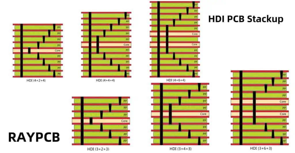
Layer Stack-up Considerations
Common Stack-up Configurations
| Stack-up Type | Layer Count | Microvia Layers | Typical Applications |
| 1-N-1 | 4.-6 | 2 | Mobile devices |
| 2-N-2 | 6.-10 | 4 | Computing |
| 3-N-3 | 8.-14 | 6 | Networking |
| Any Layer | 10+ | All | High-end systems |
Design Rules and Constraints

Component Placement
Density Guidelines
| Component Type | Minimum Pitch (mm) | Components/cm² | Escape Routing |
| BGA | 0.4-0.8 | 1.-4 | HDI Required |
| QFN | 0.4-0.5 | 4.-9 | Standard/HDI |
| 0201 Passive | 0.6 | 25-36 | Standard |
| 01005 Passive | 0.4 | 49-64 | HDI Required |
Signal Integrity Considerations
Impedance Control Parameters
| Line Type | Width (μm) | Spacing (μm) | Target Impedance (Ω) | Tolerance |
| Single-ended | 75 | 75 | 50 | ±10% |
| Differential | 75 | 75 | 100 | ±10% |
| Controlled | 100 | 100 | 75 | ±5% |
Power Distribution Optimization
Power Integrity Guidelines
Power Distribution Network (PDN) Specifications
| Parameter | Standard Design | HDI Design | Ultra HDI |
| Target Impedance (mΩ) | <500 | <250 | <100 |
| Decoupling Layers | 2.-4 | 4.-6 | 6+ |
| Plane Spacing (μm) | 100-200 | 75-100 | 50-75 |
| Via Density (/cm²) | 10月20日 | 20-40 | 40+ |
Thermal Management
Thermal Design Considerations
Thermal Solutions by Power Density
| Power Density (W/cm²) | Cooling Solution | Layer Count | Cost Impact |
| <1 | Natural convection | 4.-6 | Low |
| 1.-5 | Thermal vias | 6.-8 | Medium |
| 5.-10 | Embedded copper | 8.-12 | High |
| >10 | Advanced cooling | 12+ | Very High |
Reliability and Testing
Reliability Requirements
Test Specifications
| Test Type | Condition | Duration | Pass Criteria |
| Thermal Cycling | -40 to +125°C | 1000 cycles | No failures |
| HAST | 130°C/85% RH | 96 hours | No delamination |
| IST | -55 to +125°C | 500 cycles | <10% resistance change |
| Drop Test | 1.5m drop | 26 drops | No electrical failure |
Cost Considerations
Cost Factors by Technology Level
| Technology Level | Material Cost | Process Cost | Yield Impact | Total Factor |
| Standard PCB | 1.0x | 1.0x | 95-98% | 1.0x |
| Basic HDI | 1.3x | 1.5x | 90-95% | 1.8x |
| Advanced HDI | 1.8x | 2.0x | 85-90% | 2.5x |
| Ultra HDI | 2.5x | 3.0x | 80-85% | 3.5x |
Future Trends
Emerging Technologies
| Technology | Timeline | Impact | Challenges |
| Embedded Components | 2024-2025 | High | Process complexity |
| 3D Packaging | 2025-2026 | Very High | Thermal management |
| Optical Interconnects | 2026-2027 | Medium | Cost barriers |
| Additive Manufacturing | 2024-2025 | High | Material limitations |
Frequently Asked Questions
1. What are the key advantages of HDI technology in PCB design?
HDI technology offers several significant benefits:
- Increased routing density and reduced board size
- Improved electrical performance through shorter connections
- Better signal integrity due to smaller vias and reduced parasitics
- Enhanced thermal performance with better heat dissipation
- Greater design flexibility and component placement options These advantages make HDI essential for modern electronic devices requiring high performance in small form factors.
2. How does HDI technology impact manufacturing costs?
HDI manufacturing costs are influenced by several factors:
- More sophisticated processing equipment requirements
- Higher material costs for specialized laminates
- Increased process steps for microvia formation
- Lower yields compared to standard PCB fabrication
- More stringent quality control requirements However, these costs are often offset by the reduced board size and improved performance.
3. What are the key design considerations for HDI PCBs?
Critical design considerations include:
- Stack-up planning and impedance control
- Microvia placement and structure
- Component density and placement optimization
- Power distribution network design
- Thermal management strategies Careful attention to these factors is essential for successful HDI implementation.
4. How can reliability be ensured in HDI designs?
Reliability in HDI designs is achieved through:
- Proper material selection for the application
- Careful stack-up design and via structure planning
- Comprehensive thermal management strategies
- Thorough testing and validation procedures
- Adherence to manufacturing design rules Regular testing and validation throughout the design process is crucial.
5. What future developments are expected in HDI technology?
The future of HDI technology includes:
- Further miniaturization of features and components
- Integration of embedded components
- Advanced materials for improved performance
- 3D packaging and integration
- Novel manufacturing processes These developments will enable even greater levels of integration and performance.
Conclusion
High-Density Interconnect technology continues to evolve, pushing the boundaries of PCB miniaturization and performance. Success in HDI design requires a thorough understanding of materials, processes, and design constraints, along with careful consideration of reliability and cost factors. As electronic devices continue to demand higher performance in smaller packages, HDI technology will remain crucial for meeting these challenges. The future of HDI lies in the successful integration of emerging technologies and materials while maintaining focus on manufacturability and reliability.