In the ever-evolving world of electronics, the demand for smaller, faster, and more efficient devices continues to grow. This push for miniaturization and improved performance has led to significant advancements in printed circuit board (PCB) technology. One such innovation that has revolutionized PCB design and manufacturing is the microvia. This article will explore why microvias are superior to other types of vias, their advantages, applications, and impact on the electronics industry.
Understanding Vias in PCB Design
Before delving into the specifics of microvias, it’s essential to understand what vias are and their role in PCB design.
What is a Via?
A via is a small plated hole that connects different layers of a multi-layer PCB. Vias allow electrical signals and power to be routed between layers, enabling more complex circuit designs and efficient use of board space.
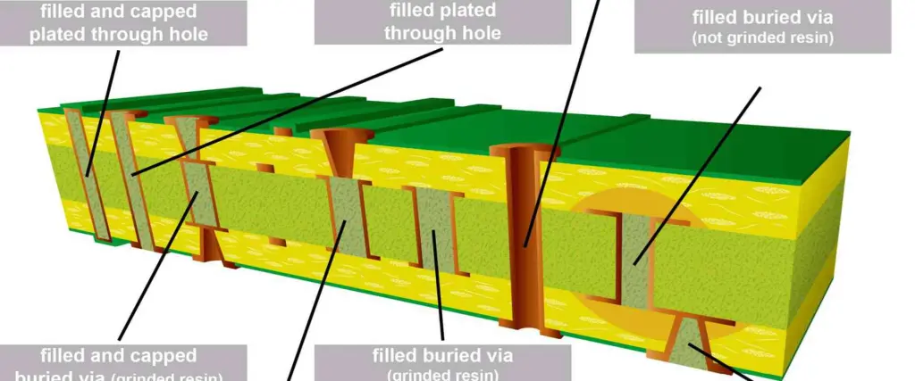
Types of Vias
There are several types of vias used in PCB design:
- Through-hole vias
- Blind vias
- Buried vias
- Microvias
Each type has its own characteristics, advantages, and limitations. However, microvias have emerged as a superior option in many applications.
Introduction to Microvias
What is a Microvia?
A microvia is a very small via with a diameter typically less than 150 micrometers (μm). These tiny interconnects are usually formed using laser drilling techniques and are designed to connect only adjacent layers of a PCB.
History and Development of Microvias
The concept of microvias was introduced in the late 1980s, but it wasn’t until the mid-1990s that they became commercially viable. The development of reliable laser drilling techniques and advances in plating technology were key factors in making microvias a practical solution for high-density interconnect (HDI) PCBs.
Advantages of Microvias Over Other Via Types
Microvias offer several significant advantages over traditional via types, making them the preferred choice for many modern electronic designs.
1. Increased Circuit Density
One of the primary advantages of microvias is their ability to significantly increase circuit density. Their small size allows for:
| Via Type | Typical Diameter | Typical Pitch |
| Through-hole | 0.3 – 0.8 mm | 1.0 – 2.5 mm |
| Blind/Buried | 0.2 – 0.6 mm | 0.8 – 2.0 mm |
| Microvia | 0.05 – 0.15 mm | 0.3 – 0.8 mm |
As the table shows, microvias allow for much tighter spacing, enabling higher component density and more complex routing options.
2. Improved Electrical Performance
Microvias contribute to better electrical performance in several ways:
- Reduced parasitic capacitance and inductance
- Shorter signal paths, leading to faster signal speeds
- Improved signal integrity due to reduced reflections and crosstalk
These factors are particularly crucial in high-speed digital designs and RF applications.
3. Enhanced Reliability
Contrary to what one might expect from their small size, microvias often offer improved reliability compared to larger vias:
- Less thermal stress due to smaller size and reduced copper mass
- Improved plating uniformity, reducing the risk of voids or weak spots
- Better adhesion to the substrate due to the laser drilling process
4. Design Flexibility
Microvias provide designers with greater flexibility in PCB layout:
- Ability to place vias directly on component pads (via-in-pad design)
- Easier routing around densely packed components
- More options for signal and power distribution
5. Cost-Effective for High-Density Designs
While the initial cost of microvia technology may be higher, it becomes cost-effective for high-density designs:
- Reduced overall board size
- Fewer PCB layers required for complex designs
- Higher yield rates in production due to improved reliability
Microvia Formation Techniques
The superior performance of microvias is largely due to the advanced techniques used in their formation.
Laser Drilling
Laser drilling is the most common method for creating microvias. It offers several advantages:
- Precise control over via diameter and depth
- Ability to create very small vias (down to 25 μm in some cases)
- Clean, consistent hole formation
Photovia Process
Some manufacturers use a photovia process, which involves:
- Applying a photo-imageable dielectric
- Exposing and developing to create via holes
- Plating to form the electrical connection
This process can be cost-effective for large-scale production.
Plasma Etching
Plasma etching is sometimes used for microvia formation, particularly in certain flexible PCB applications. It offers:
- Good control over via shape
- Ability to create tapered vias for improved plating
Microvia Structures and Stacking

Microvias can be used in various configurations to meet different design requirements.
Single-Layer Microvias
The simplest form, connecting two adjacent layers.
Stacked Microvias
Multiple microvias stacked on top of each other, connecting several layers.
Staggered Microvias
Microvias that are offset from each other, useful for complex routing scenarios.
| Structure | Description | Best Used For |
| Single-Layer | Connects two adjacent layers | Simple HDI designs |
| Stacked | Multiple microvias stacked vertically | High layer count boards |
| Staggered | Offset microvias | Complex signal routing |
Applications of Microvias
The advantages of microvias make them ideal for a wide range of applications, particularly in industries where size, performance, and reliability are crucial.
Consumer Electronics
- Smartphones
- Tablets
- Wearable devices
Automotive Electronics
- Advanced driver-assistance systems (ADAS)
- Infotainment systems
- Electric vehicle control units
Aerospace and Defense
- Satellite communications
- Radar systems
- Avionics
Medical Devices
- Implantable devices
- Portable diagnostic equipment
- High-resolution imaging systems
Telecommunications
- 5G infrastructure
- Optical networking equipment
- High-speed routers and switches
Challenges and Considerations in Microvia Implementation
While microvias offer numerous advantages, their implementation does come with certain challenges that need to be addressed.
1. Manufacturing Complexity
Producing PCBs with microvias requires specialized equipment and expertise:
- High-precision laser drilling systems
- Advanced plating techniques
- Stringent process control
2. Cost Considerations
The initial investment in microvia technology can be significant:
- Higher tooling costs
- More expensive raw materials (high-performance laminates)
- Potentially longer production times
3. Design Rules and Constraints
Microvia designs must adhere to specific rules to ensure manufacturability and reliability:
- Minimum via diameter and pitch
- Aspect ratio limitations
- Stack-up considerations for multi-layer microvias
4. Testing and Inspection
Ensuring the quality and reliability of microvias requires advanced testing and inspection methods:
- X-ray inspection for internal structures
- Electrical testing for connectivity
- Cross-sectioning for process verification
Future Trends in Microvia Technology

As technology continues to advance, we can expect further developments in microvia technology:
1. Even Smaller Vias
Research is ongoing to develop reliable sub-25 μm vias, enabling even higher density designs.
2. New Materials
Development of new laminate and conductive materials optimized for microvia performance and reliability.
3. Improved Manufacturing Processes
Advancements in laser technology and plating processes to increase efficiency and reduce costs.
4. Integration with Additive Manufacturing
Exploring ways to incorporate microvia technology with 3D printed electronics for novel form factors and applications.
Impact on the Electronics Industry
The adoption of microvia technology has had a profound impact on the electronics industry:
Enabling Miniaturization
Microvias have been a key enabler in the trend towards smaller, thinner electronic devices.
Improving Performance
The electrical characteristics of microvias have contributed to the increased speed and performance of modern electronics.
Enhancing Reliability
The reliability improvements offered by microvias have increased the overall quality and lifespan of electronic products.
Driving Innovation
The capabilities provided by microvia technology have opened up new possibilities in product design and functionality.
Conclusion
Microvias have proven to be superior to other via types in many aspects, particularly for high-density, high-performance electronic designs. Their ability to increase circuit density, improve electrical performance, enhance reliability, and provide design flexibility makes them an invaluable tool in modern PCB design.
While the implementation of microvia technology does come with challenges, particularly in terms of manufacturing complexity and initial costs, the benefits often outweigh these concerns, especially as the technology continues to mature and become more accessible.
As we look to the future, microvias will undoubtedly play a crucial role in enabling the next generation of electronic devices. From ever-smaller consumer gadgets to advanced medical implants and cutting-edge aerospace systems, microvia technology will continue to push the boundaries of what’s possible in electronic design.
The superiority of microvias over other via types is not just about their size; it’s about the new possibilities they open up. As the electronics industry continues to evolve, embracing microvia technology will be essential for companies looking to stay at the forefront of innovation and meet the ever-increasing demands for smaller, faster, and more reliable electronic products.
Frequently Asked Questions (FAQ)
1. Are microvias suitable for all types of PCB designs?
While microvias offer significant advantages, they are not necessary or cost-effective for all PCB designs. Microvias are most beneficial in high-density designs where space is at a premium, or in high-speed applications where signal integrity is crucial. For simpler, low-density boards or those with less stringent performance requirements, traditional through-hole or larger blind/buried vias may be more appropriate and cost-effective.
2. How do microvias affect the overall cost of PCB production?
The impact of microvias on PCB production cost can vary:
- Initial Costs: Implementing microvia technology often increases initial production costs due to the need for specialized equipment and processes.
- Volume Production: For high-volume production, the cost per board can decrease as the setup costs are spread over more units.
- Design Complexity: In complex, high-density designs, microvias can actually reduce overall costs by allowing for smaller board sizes and fewer layers.
- Long-term Benefits: Improved reliability and performance can lead to cost savings over the product lifecycle.
It’s important to conduct a cost-benefit analysis for each specific application to determine if microvia technology is economically viable.
3. What are the main challenges in designing PCBs with microvias?
Designing PCBs with microvias presents several challenges:
- Adherence to strict design rules (minimum diameters, aspect ratios, etc.)
- Careful stackup planning to optimize layer transitions
- Consideration of manufacturing tolerances and capabilities
- Balancing signal integrity requirements with design density
- Managing thermal issues in high-density areas
Designers need to work closely with manufacturers to ensure that their designs are both optimal and producible.
4. How reliable are microvias compared to traditional vias?
When properly designed and manufactured, microvias can be more reliable than traditional vias:
- Less thermal stress due to smaller size
- Improved plating uniformity
- Better adhesion to the substrate
However, reliability can be affected by factors such as:
- Quality of the manufacturing process
- Design choices (e.g., stacked vs. staggered microvias)
- Operating conditions of the final product
It’s crucial to follow best practices in design and work with experienced manufacturers to ensure optimal reliability.
5. Can existing PCB designs be converted to use microvias?
Converting existing PCB designs to use microvias is possible, but it’s not always straightforward:
- Redesign Effort: Significant redesign may be required to take full advantage of microvia capabilities.
- Performance Gains: The conversion can lead to improved performance and reduced board size.
- Cost Considerations: The redesign and new manufacturing processes may increase costs initially.
- Compatibility: Ensure that all components are compatible with the new design.
Before converting, it’s important to assess whether the benefits of microvias justify the redesign effort for the specific application. In many cases, it may be more efficient to incorporate microvia technology in new designs rather than retrofitting existing ones.