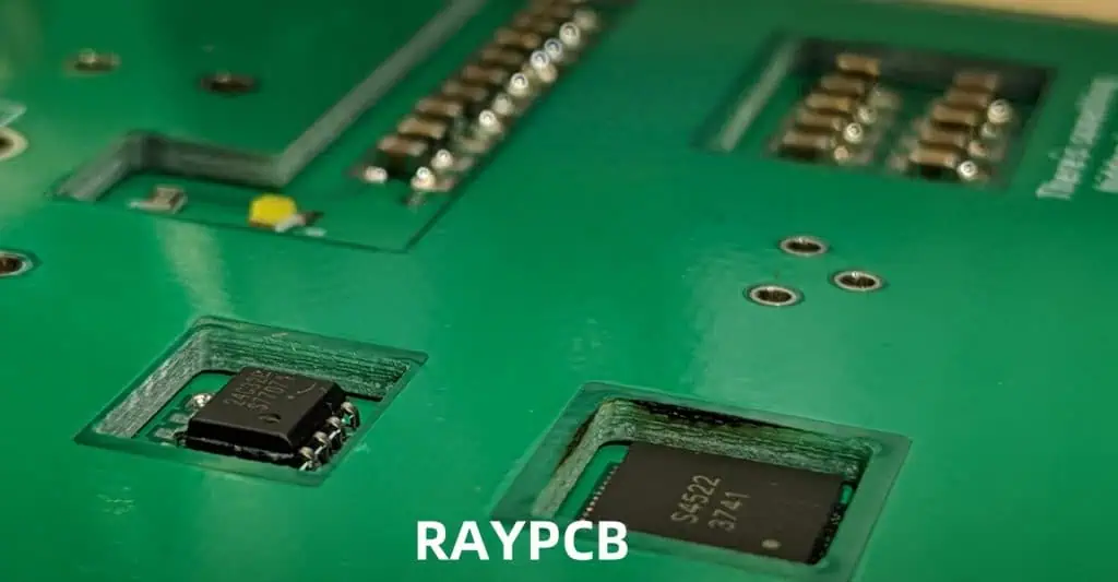
Printed Circuit Boards (PCBs) are the backbone of modern electronics, providing a sturdy foundation for components and facilitating electrical connections between them. As electronic devices become increasingly complex and compact, PCB designers are constantly seeking innovative ways to optimize board performance and space utilization. One such innovation that has gained significant traction in recent years is the concept of Buried Capacitance PCB.
In this comprehensive article, we will delve deep into the world of Buried Capacitance PCB technology, exploring its definition, principles, advantages, challenges, and applications. We’ll also discuss how this technology compares to traditional PCB designs and examine its impact on the electronics industry as a whole.
Understanding Buried Capacitance PCB

Definition and Basic Concept
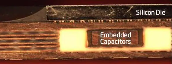
Buried Capacitance PCB, also known as embedded capacitance or power-ground laminate technology, is an advanced PCB design technique that integrates capacitance directly into the board structure. This is achieved by creating an extremely thin dielectric layer between power and ground planes within the PCB stack-up.
The fundamental principle behind buried capacitance is based on the basic formula for capacitance:
CopyC = ε * A / d
Where:
- C is the capacitance
- ε is the dielectric constant of the material
- A is the area of the conductive plates
- d is the distance between the plates
By minimizing the distance between power and ground planes and using materials with high dielectric constants, PCB designers can create significant capacitance within the board itself.
Historical Context
The concept of buried capacitance in PCBs emerged in the late 1990s as a response to the increasing challenges posed by high-speed digital circuits. As clock speeds and edge rates increased, traditional discrete decoupling capacitors began to show limitations in their ability to suppress noise and maintain power integrity.
The development of buried capacitance technology was driven by the need for:
- Improved power distribution
- Enhanced signal integrity
- Reduced electromagnetic interference (EMI)
- More efficient use of PCB real estate
Over the years, the technology has evolved and matured, finding applications in various industries, from consumer electronics to aerospace and defense.
How Buried Capacitance PCB Works
Physical Structure
A typical buried capacitance PCB incorporates the following key elements:
- Power plane
- Ultra-thin dielectric layer (usually less than 10 μm)
- Ground plane
These layers are typically placed near the center of the PCB stack-up, surrounded by signal layers and additional power/ground planes as needed.
Electrical Characteristics
The buried capacitance structure exhibits several important electrical characteristics:
- Low inductance: Due to the extremely short current path between power and ground planes, the inductance is significantly reduced compared to discrete capacitors.
- Distributed capacitance: The capacitance is spread evenly across the entire board area, providing more uniform decoupling.
- High-frequency performance: The low inductance and distributed nature of buried capacitance make it effective at suppressing high-frequency noise.
- Reduced impedance: The power distribution network (PDN) impedance is lowered, improving overall system performance.
Comparison with Traditional Decoupling Methods
To better understand the advantages of buried capacitance, let’s compare it with traditional decoupling methods:
| Characteristic | Traditional Decoupling | Buried Capacitance |
| Component Count | High (many discrete capacitors) | Low (integrated into PCB) |
| Board Space | Significant space required | Minimal impact on board space |
| Effectiveness at High Frequencies | Limited by parasitic inductance | Highly effective |
| Uniformity of Decoupling | Localized | Distributed across the board |
| Design Complexity | Can be complex (placement optimization) | Simplified design process |
| Cost | Variable (depends on component count) | Higher initial cost, po |
Advantages of Buried Capacitance PCB
Improved Signal Integrity
One of the primary benefits of buried capacitance PCB is the significant improvement in signal integrity. This is achieved through:
- Reduced ground bounce: The low-impedance power distribution network minimizes voltage fluctuations.
- Decreased crosstalk: The tighter coupling between power and ground planes reduces electromagnetic interference between signal traces.
- Better return path: The continuous ground plane provides an optimal return path for high-speed signals.
Enhanced Power Integrity
Buried capacitance technology offers several advantages for power integrity:
- Lower PDN impedance: The distributed capacitance reduces the overall impedance of the power distribution network.
- Improved transient response: The low-inductance path between power and ground planes allows for faster charge delivery to switching components.
- Reduced voltage ripple: The integrated decoupling helps maintain a more stable supply voltage across the board.
Space Savings and Component Reduction
By integrating capacitance into the PCB structure, designers can:
- Eliminate or reduce the number of surface-mounted decoupling capacitors.
- Free up valuable board space for additional components or further miniaturization.
- Simplify the PCB assembly process by reducing the number of components to be placed.
EMI Reduction
Buried capacitance PCBs contribute to reduced electromagnetic interference (EMI) through:
- Lower ground plane impedance, which minimizes common-mode radiation.
- Reduced current loop areas, decreasing the antenna effect of PCB traces.
- Improved shielding effectiveness due to the tightly coupled power and ground planes.
Reliability Improvements
The use of buried capacitance can enhance overall system reliability:
- Fewer solder joints: With fewer discrete components, there are fewer potential points of failure.
- Reduced thermal stress: The elimination of surface-mounted capacitors can lead to more even heat distribution.
- Improved resistance to mechanical stress: The integrated nature of buried capacitance makes it less susceptible to vibration and shock.
Design Considerations for Buried Capacitance PCB
Material Selection
Choosing the right materials is crucial for effective buried capacitance implementation:
- Dielectric material: High-k materials are preferred to maximize capacitance.
- Copper foil: Ultra-thin copper foils are often used to minimize the distance between planes.
- Prepreg and core materials: These must be compatible with the thin dielectric and copper layers.
Stack-up Design
Careful consideration of the PCB stack-up is essential:
- Placement of buried capacitance layers: Typically near the center of the stack-up for optimal performance.
- Signal layer arrangement: Proper distribution of signal layers around the buried capacitance structure.
- Impedance control: Adjusting trace widths and spacings to maintain desired impedances.
Power Plane Design
Effective power plane design is critical for maximizing the benefits of buried capacitance:
- Partitioning: Separating different voltage domains while maintaining capacitive coupling.
- Void management: Minimizing voids in the power plane to ensure uniform capacitance.
- Current capacity: Ensuring sufficient copper weight to handle the required current.
Simulation and Modeling
Advanced simulation tools are often necessary to optimize buried capacitance designs:
- 3D electromagnetic simulation: For accurate modeling of the complex PCB structure.
- Power integrity analysis: To verify PDN performance and identify potential issues.
- Signal integrity simulation: To ensure that high-speed signals maintain their integrity.
Challenges and Limitations
Manufacturing Complexities
Buried capacitance PCBs present several manufacturing challenges:
- Thin material handling: Working with ultra-thin dielectrics requires specialized equipment and processes.
- Registration accuracy: Precise alignment of layers is crucial for consistent capacitance.
- Yield considerations: The complexity of the process can lead to lower yields, especially in early implementations.
Cost Considerations
While buried capacitance can offer long-term cost benefits, there are initial cost hurdles:
- Higher material costs: Specialized materials for buried capacitance are often more expensive.
- Increased manufacturing costs: The complex process and potential for lower yields can drive up production costs.
- Design costs: Additional time and expertise required for optimizing buried capacitance designs.
Design Tool Limitations
Many existing PCB design tools may not fully support buried capacitance technology:
- Stack-up definition: Some tools may struggle with ultra-thin layers in the stack-up.
- Capacitance calculation: Accurate modeling of distributed capacitance can be challenging.
- Design rule checking: Specialized rules for buried capacitance may not be readily available.
Performance Limitations
While buried capacitance offers many advantages, it’s not a universal solution:
- Frequency limitations: There’s an upper limit to the frequency range where buried capacitance is effective.
- Capacitance density: The achievable capacitance per unit area may be lower than with some discrete components.
- Voltage limitations: The thin dielectric layers may limit the maximum operating voltage.
Applications of Buried Capacitance PCB
High-Speed Digital Systems
Buried capacitance technology finds extensive use in high-speed digital applications:
- Servers and data centers: Where signal integrity and power distribution are critical.
- Telecommunications equipment: For handling high-speed data transmission.
- High-performance computing: To support the demands of advanced processors and memory systems.
RF and Microwave Circuits
The low-inductance characteristics of buried capacitance make it valuable in RF applications:
- Wireless communication devices: For improved signal quality and reduced interference.
- Radar systems: To enhance sensitivity and reduce noise.
- Satellite communications: Where space and weight savings are crucial.
Aerospace and Defense
The reliability and performance benefits of buried capacitance are particularly valuable in aerospace:
- Avionics systems: For enhanced reliability in critical flight control systems.
- Satellite electronics: Where size, weight, and power (SWaP) optimization is essential.
- Military communications: For improved EMI resistance and signal security.
Consumer Electronics
As consumer devices become more compact and powerful, buried capacitance offers advantages:
- Smartphones and tablets: Enabling more features in smaller form factors.
- Wearable devices: Where space savings and power efficiency are paramount.
- High-end audio equipment: For improved signal purity and noise reduction.
Automotive Electronics
The automotive industry is increasingly adopting buried capacitance technology:
- Advanced driver assistance systems (ADAS): For reliable, high-speed signal processing.
- Infotainment systems: To manage complex multimedia and connectivity features.
- Electric vehicle control systems: For efficient power management and noise reduction.
Future Trends and Developments
Material Advancements
Ongoing research in materials science is likely to yield improvements:
- Higher-k dielectrics: To achieve greater capacitance density.
- Thinner and more robust materials: For improved performance and manufacturability.
- Novel composite materials: Combining electrical and thermal management properties.
Integration with Other Technologies
Buried capacitance is likely to be combined with other advanced PCB technologies:
- Embedded active and passive components: Further miniaturization and performance improvements.
- 3D printed electronics: Potential for customized, high-performance buried capacitance structures.
- Flexible and stretchable electronics: Adapting buried capacitance concepts to non-rigid substrates.
Design Tool Evolution
PCB design software is expected to evolve to better support buried capacitance:
- Improved simulation capabilities: More accurate modeling of distributed capacitance effects.
- Automated optimization: Tools to help designers maximize the benefits of buried capacitance.
- Integration with AI and machine learning: For more efficient and effective PCB designs.
Standardization Efforts
As the technology matures, we can expect to see:
- Industry standards: Defining best practices for buried capacitance implementation.
- Testing and qualification procedures: Ensuring reliability and performance consistency.
- Design guidelines: Helping engineers effectively incorporate buried capacitance in their designs.
Conclusion
Buried Capacitance PCB technology represents a significant advancement in the field of electronic design, offering a range of benefits including improved signal and power integrity, space savings, and enhanced reliability. While it presents some challenges in terms of manufacturing complexity and initial costs, the advantages it offers make it an increasingly attractive option for a wide range of applications.
As the technology continues to evolve and mature, we can expect to see even greater adoption across various industries, from consumer electronics to aerospace and defense. The ongoing developments in materials science, design tools, and manufacturing processes will likely address many of the current limitations, further expanding the potential of buried capacitance PCB technology.
For engineers and PCB designers, understanding and leveraging buried capacitance technology will be crucial in creating the next generation of high-performance, compact, and reliable electronic systems. As we move towards an increasingly connected and digital world, the role of advanced PCB technologies like buried capacitance will only grow in importance, enabling the innovative devices and systems that will shape our future.
Frequently Asked Questions (FAQ)
1. What is the main difference between buried capacitance and traditional decoupling methods?
The main difference lies in how capacitance is implemented. Traditional decoupling methods use discrete capacitors soldered onto the PCB surface, while buried capacitance integrates the capacitance directly into the PCB structure using extremely thin dielectric layers between power and ground planes. This results in distributed, low-inductance capacitance that is effective at higher frequencies and doesn’t consume valuable board space.
2. Is buried capacitance PCB technology suitable for all types of electronic designs?
While buried capacitance offers significant advantages, it’s not necessarily suitable or cost-effective for all designs. It’s most beneficial in high-speed digital systems, RF applications, and designs where space is at a premium. For simpler, low-speed designs or where cost is the primary concern, traditional PCB designs with discrete components may still be more appropriate.
3. How does buried capacitance PCB affect the overall cost of a product?
The cost impact of buried capacitance PCB is complex. Initially, it may increase costs due to more expensive materials and manufacturing processes. However, it can lead to cost savings in other areas, such as reduced component count, simplified assembly, and improved reliability. The overall cost-effectiveness depends on the specific application, production volume, and long-term reliability requirements.
4. Can buried capacitance completely eliminate the need for discrete decoupling capacitors?
In most cases, buried capacitance significantly reduces the need for discrete decoupling capacitors but doesn’t entirely eliminate it. Some designs may still require a few strategically placed discrete capacitors to handle specific frequency ranges or provide localized decoupling for sensitive components. The exact balance depends on the specific design requirements and performance goals.
5. What are the key challenges in manufacturing buried capacitance PCBs?
The main challenges in manufacturing buried capacitance PCBs include:
- Handling and processing ultra-thin dielectric materials
- Achieving precise registration and alignment of layers
- Maintaining consistent quality and yield, especially for large board sizes
- Managing the increased complexity of the PCB stack-up
- Implementing effective testing and quality control procedures for the buried capacitance structure
These challenges require specialized equipment, expertise, and careful process control to overcome.