Printed Circuit Boards (PCBs) are the backbone of modern electronics, serving as the foundation for countless devices we use daily. However, the manufacturing process of PCBs is complex and prone to various defects, with voids being one of the most challenging issues. Voids are empty spaces or cavities that can form within solder joints or other areas of a PCB, potentially compromising the board’s reliability and performance. This article delves into the causes of voids, their impact on PCB functionality, and most importantly, the strategies to prevent them during the manufacturing process.
Understanding Voids in PCBs
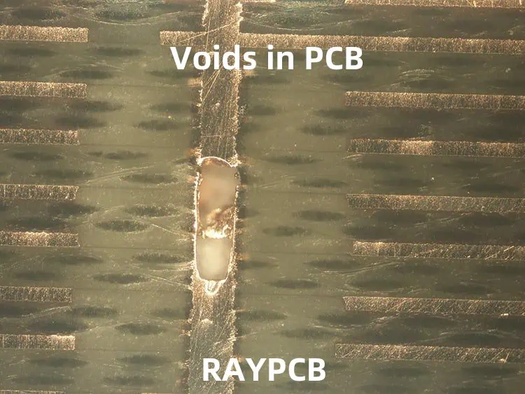
What Are Voids?
Voids are unintended empty spaces or air pockets that can occur within solder joints, between layers of the PCB, or in other critical areas during the manufacturing process. These voids can vary in size, from microscopic bubbles to larger cavities that are visible to the naked eye.
Types of Voids
1. Solder Voids

Solder voids are the most common type, occurring within solder joints. They can be further classified into:
- Macro voids: Larger voids typically caused by outgassing during the reflow process
- Micro voids: Smaller voids often resulting from flux residues or contamination
- Planar voids: Voids that form at the interface between the solder and the pad or component
2. Laminate Voids
These voids occur between the layers of the PCB laminate, often due to issues in the lamination process or contamination of prepreg materials.
3. Plated Through-Hole (PTH) Voids
Voids that form within plated through-holes, potentially affecting the electrical connections between layers.
Impact of Voids on PCB Performance
Voids can have several detrimental effects on PCB performance and reliability:
- Reduced electrical conductivity
- Increased thermal resistance
- Weakened mechanical strength
- Potential for short circuits or open circuits
- Reduced overall reliability and lifespan of the PCB
Causes of Voids in PCB Manufacturing
Understanding the root causes of void formation is crucial for developing effective prevention strategies. Here are the primary factors contributing to void formation:
1. Outgassing
Outgassing occurs when volatile components in solder paste, flux, or PCB materials vaporize during the heating process. These vapors can become trapped, forming voids.
2. Moisture Absorption
PCB materials and components can absorb moisture from the environment. During the soldering process, this moisture rapidly expands, creating voids.
3. Contamination
Surface contaminants, such as oils, dust, or residues from the manufacturing process, can interfere with proper solder wetting and lead to void formation.
4. Improper Reflow Profile
An incorrect temperature profile during the reflow soldering process can prevent proper outgassing and lead to void entrapment.
5. Solder Paste Quality and Application
The quality of solder paste and how it’s applied can significantly impact void formation. Issues such as inconsistent paste deposition or the use of expired paste can increase the likelihood of voids.
6. PCB Surface Finish
The type and quality of the PCB surface finish can affect solder wetting and potentially contribute to void formation.
7. Component Design
Certain component designs, particularly those with large flat surfaces or bottom-terminated components (BTCs), are more prone to void formation.
Strategies for Preventing Voids
Preventing voids requires a multifaceted approach that addresses various stages of the PCB manufacturing process. Here are key strategies to minimize void formation:
1. Material Selection and Handling
Choose Low-Moisture Absorption Materials
Select PCB materials with low moisture absorption properties to reduce the risk of moisture-related voids.
Proper Storage and Handling
Store PCB materials, components, and solder paste in controlled environments to prevent moisture absorption and contamination.
2. Design Considerations
Optimized Pad Design
Design pads with appropriate size and shape to promote proper solder wetting and reduce the likelihood of void formation.
Thermal Relief Patterns
Implement thermal relief patterns to manage heat distribution during soldering, reducing the risk of overheating and outgassing.
3. Solder Paste Selection and Application
High-Quality Solder Paste
Use high-quality, fresh solder paste with appropriate flux content and metal load for the specific application.
Optimized Stencil Design
Design stencils with appropriate aperture sizes and shapes to ensure proper solder paste deposition.
Controlled Paste Deposition
Utilize advanced printing techniques and equipment to achieve consistent and controlled solder paste deposition.
4. Reflow Profile Optimization
Customized Reflow Profiles
Develop and optimize reflow profiles specific to the PCB design, components, and materials used.
Proper Preheat and Soak Stages
Implement adequate preheat and soak stages to allow for controlled outgassing and moisture evaporation.
Optimized Peak Temperature and Time
Carefully control peak temperature and time above liquidus to ensure proper solder wetting while minimizing the risk of excessive outgassing.
5. Surface Preparation and Cleanliness

Thorough Cleaning
Implement rigorous cleaning processes to remove contaminants from PCB surfaces and components.
Surface Activation
Use appropriate surface activation techniques to enhance solder wetting and reduce the risk of void formation.
6. Advanced Manufacturing Techniques
Vacuum Reflow Soldering
Utilize vacuum reflow soldering systems to actively remove gases and reduce void formation during the soldering process.
Vapor Phase Soldering
Consider vapor phase soldering for its uniform heating properties and ability to reduce oxidation during the soldering process.
7. Quality Control and Inspection
X-ray Inspection
Implement X-ray inspection techniques to detect and analyze voids in solder joints and other critical areas.
Process Monitoring and Control
Utilize advanced process monitoring tools to track key parameters and maintain consistent manufacturing conditions.
Void Acceptance Criteria and Industry Standards
While complete elimination of voids is often impractical, industry standards provide guidelines for acceptable void levels. The following table summarizes some common void acceptance criteria:
| Standard | Application | Maximum Void Percentage |
| IPC-A-610 Class 3 | High-reliability electronics | 25% for BGA, 15% for other components |
| IPC-7095 | BGA assemblies | 25% cumulative void area |
| JEDEC JESD22-B106 | Thermal voids in power devices | 50% of total pad area |
It’s important to note that specific industries or applications may have more stringent requirements, and manufacturers should always refer to the most up-to-date standards and customer specifications.
Case Study: Implementing Void Prevention Strategies
To illustrate the effectiveness of void prevention strategies, let’s consider a case study of a high-reliability electronics manufacturer facing challenges with void formation in their PCB assemblies.
Background
- The manufacturer was experiencing a high rejection rate due to excessive voids in BGA solder joints.
- X-ray inspection revealed void percentages ranging from 30% to 40% in affected assemblies.
- The issue was particularly prevalent in a new product line featuring large BGAs with high I/O counts.
Implemented Solutions
- Material and Component Management
- Implemented strict moisture control procedures, including the use of dry cabinets for PCB and component storage.
- Reduced maximum floor life of moisture-sensitive components and implemented baking procedures when necessary.
- Solder Paste Optimization
- Switched to a low-voiding solder paste formulation specifically designed for BGA applications.
- Implemented refrigerated storage and automated paste dispensing to ensure consistent paste quality.
- Stencil Design
- Redesigned stencils with optimized apertures for BGA pads, including the use of multi-level stencils for critical areas.
- Reflow Profile Optimization
- Developed custom reflow profiles for each product, with extended preheat and soak stages to promote controlled outgassing.
- Implemented nitrogen atmospheres in reflow ovens to improve wetting and reduce oxidation.
- Process Monitoring and Control
- Installed advanced paste inspection systems to ensure consistent solder paste deposition.
- Implemented real-time thermal profiling for each production run to maintain optimal reflow conditions.
Results
After implementing these strategies over a six-month period, the manufacturer observed the following improvements:
| Metric | Before Implementation | After Implementation |
| Average Void Percentage | 35% | 12% |
| Rejection Rate | 15% | 2% |
| Product Reliability (MTBF) | 50,000 hours | 75,000 hours |
| Customer Returns | 5% | 0.50% |
This case study demonstrates the significant impact that comprehensive void prevention strategies can have on PCB manufacturing quality and overall product performance.
Conclusion
Preventing voids during PCB manufacture is a critical aspect of ensuring the reliability and performance of electronic devices. By understanding the causes of voids and implementing a comprehensive set of prevention strategies, manufacturers can significantly reduce void formation and improve overall product quality. Key to success is a holistic approach that addresses material selection, design considerations, process optimization, and rigorous quality control.
As technology continues to advance and PCB designs become increasingly complex, the importance of void prevention will only grow. Staying informed about the latest research, technologies, and best practices in this field will be essential for manufacturers looking to maintain a competitive edge in the electronics industry.
Frequently Asked Questions (FAQ)
- Q: What is the acceptable level of voids in PCB solder joints? A: The acceptable level of voids varies depending on the application and industry standards. Generally, for high-reliability electronics, voids should not exceed 25% of the total joint area for BGAs and 15% for other components, according to IPC-A-610 Class 3 standards. However, some applications may require even lower void percentages.
- Q: Can voids in PCBs be repaired after manufacture? A: In most cases, voids within solder joints are difficult to repair after manufacture without risking damage to the PCB or components. Prevention is the best approach. However, for severe cases, techniques such as rework or reballing of BGA components might be considered, but these processes carry their own risks and should be performed by skilled technicians.
- Q: How effective is vacuum reflow soldering in reducing voids? A: Vacuum reflow soldering can be highly effective in reducing voids, often achieving void reductions of 50% to 90% compared to standard reflow processes. However, the effectiveness can vary depending on factors such as solder paste formulation, component type, and specific process parameters.
- Q: Are there any new technologies on the horizon for void prevention in PCB manufacturing? A: Yes, several promising technologies are being developed or refined, including advanced solder paste formulations with nano-coatings, AI-driven reflow profile optimization, and new inspection techniques using high-resolution CT scanning. Additionally, research into novel PCB materials with inherently low outgassing properties is ongoing.
- Q: How does moisture sensitivity level (MSL) relate to void formation in PCBs? A: Moisture Sensitivity Level (MSL) is directly related to the potential for void formation. Components with higher MSL ratings are more prone to absorbing moisture, which can lead to void formation during the reflow process. Proper handling and storage of moisture-sensitive components, including baking when necessary, is crucial for preventing moisture-related voids.