Printed circuit boards (PCBs) form the basis of all electronic products, connecting multiple components together in one substrate to realize complex functionality. While large-scale commercial PCB production works for final products, it is not feasible for quick design iterations during prototyping phase.
This is where DIY PCB etching kits empower hobbyists and electronics innovators to fabricate PCB samples rapidly at home or makerspaces without huge equipment investments. They provide all necessary materials and simplified tools compared to setting up industrial grade etching machinery.
This guide covers PCB etching kit options, making suitable kits selection, usage guidance and tips to maximize utility.
Benefits of Using a PCB Etching Kit
Constructing PCBs manually using etching kits offers several advantages over commodity PCB production during design development cycles:
Faster Turnaround – Produce test boards within hours instead of waiting days for commercial fab house delivery
Lower Costs – Avoid paying for shipping, panelizing or minimum order quantities
Design Iteration – Validate, tweak and re-fabricate boards frequently as layout evolves
Customization – Flexible DIY process supports any copper thickness, substrate material or shape
Educational – Hands-on learning about inner workings of PCB creation process
Hence starter etching kits equip electronics enthusiasts with affordable in-house rapid prototyping capabilities.
Working Principle of PCB Etching Kits
Let’s understand the core mechanisms of how etching kits work to transfer electronic circuit layouts onto blank boards:
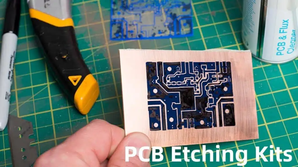
A PCB etching kit enables selectively dissolving copper cladding from laminate boards surface using etchant liquids to leave behind just intended conductor pattern defined under a protective resist layer.
Similar to photographic prints emerging when exposed areas of photo papers dissolve, etching removes unwanted copper exposing the masked printed wiring layout.
The DIY etching kit provides all necessary materials and accessories in a ready kit format to perform this key circuit patterning process before electronic components can be soldered.
Underlying approach involves:
- Start with copper clad laminate PCB blank
- Print layout plan on resist coating using laser/inkjet
- Etch-resistant resist layer masks areas to retain copper
- Etchant dissolves exposed copper surface cleanly
- Resist stripped off leaving just circuit conductors
Now let us explore popular etching kit options available.

Types of PCB Etching Kits
A multitude of etching kits exist to meet different needs and budgets. Broad categorizations are:
Complete Starter Kit
All inclusive kits with materials, tools and instructions for new users:
- Copper clad boards
- Etchant chemicals
- Etch resist pens/film
- Protective gear
- Processing trays, holders etc
Economy Component Kit
Contains just the chemicals and stock boards:
- Ferric chloride crystals
- Marker ink resist pen
- Copper laminate sheet
Premium Kit
Improved components for faster, cleaner results
- High capability etchant concentrate
- Laminator for dry film resist
- Pre-sensitized PCB blanks
- Reusable etchant container
We will explore popular options across these kit variants.
Selecting Suitable Etching Kits
With myriad kit choices available, how do you pick the right DIY etching system matching needs?
Consider these aspects when deciding appropriate PCB etching starter kit:
Budget – Complete kits cost higher but have built-in instructions and components. Economy kits need supplementary tools purchased separately.
Safety – Check etchant type and included protective equipment compatibility. Eye shield, gloves etc minimize risks.
PCBs Produced – Required copper thickness, board sizes supported, resolution capability etc.
Repeat Usage – Reusable components allow frequent prototyping. Single-use kits offer limited runs.
Convenience – Pre-treated boards and simplified tools choose ease of use over customization.
Scalability – Upgrade potential to higher volume production determines extended utility.
With these parameters in mind, let’s examine popular PCB etching kit composition available for home users and schools.
Top Etching Kits List with Details
Here is a curation of versatile PCB etching starters kit covering entry-level to advanced user needs:
1. Gikfun EK8508 Complete Kit
All-in-one inclusive kit contains materials, tools and instructions for beginners:
- FeCl Ferric chloride etchant sachets
- 10 PCB copper clad boards
- Inkjet film and laser toner transfer
- Etchant tank, eye shield, gloves
- Transfer paper, tweezers, tapes
Best for: Complete newbie packages. Replenishable etchant and boards.
2. geeetech Double-sided Kit
Economical starter bundle with chemicals and supplies:
- Ammonium persulfate etchant
- 10 double-sided copper boards
- Laser printer transparency film
- Marker ink resist pen
- Powder developer
Best for: Cost-effective starter kit. Safer etchant.
3. HiLetgo Professional Etching System
Advanced etching system for premium results:
- High speed etchant concentrate
- Laminator applicator
- 10 photosensitive PCB blanks
- Etchant tank, pump, tubing
- Tweezers, transfer film
Best for: Superior quality PCBs. Reusable equipment.
4. VoBan TE899 Glass Etching Tank Kit
Refillable glass tank with etching production capabilities:
- 1 liter glass tank
- Chemical resistance etchant
- Submersible pump
- PVC tubing, filter, lid
- Blank PCB panels
Best for: Upgradable to high volume etching. Robust receptacle.
5. MG Chemicals Ferric Chloride Kit
Commercial grade vertical etching system:
- High purity FeCl3 etchant
- Reusable PP tank
- Basket for vertical dipping
- Copper clad laminate boards
- Transfer film, gloves, instructions
Best for: Superior etching performance. Reusable tank.
This wide variety allows selecting DIY PCB etching kits precisely tailored to skill levels, accuracy needs and usage scales etc. Even basic kits facilitate affordable prototyping while premium offerings help scale limits.
How to Use PCB Etching Kits
We will outline general steps in using the DIY etching method to fabricate custom printed circuit boards successfully:
Step 1 – Design Circuit Layout
- Create copper layout plan for target board using CAD
- Print transparency film image for photoresist transfer
Step 2 – Prepare Copper Board
- Select etched copper clad laminate board with desired thickness
- Clean PCB surface completely ensuring degreased
Step 3 – Apply Etch Resist
- Cover board with dry film photoresist using hot laminator
- Run transparency film print exposed to UV light
- Alternatively directly draw layout using etch resist markers
Step 4 – Mix and Heat Etchant
- Prepare ferric chloride solution at suitable concentration
- Pour etchant into kit tank and heat to 30-45°C
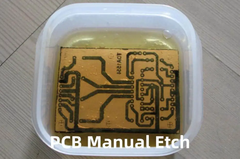
Step 5 – Immerse Board in Etchant
- Position masked PCB into etchant bath using kit holders
- Agitate boards constantly monitoring progress
Step 6 – Clean and Finish
- Retrieve board after etching completes
- Wash off resist coating under water spray
- Check for unetched spots and repeat if needed
This forms ready-to-use PCB substrate with copper tracks in desired electrical layout ready for drilling holes and populating components to build circuits.
Tips for Using DIY Etching Kits
Here are some suggestions to use etching starter kits effectively:
Safety First
- Wear eye shield, gloves, work in ventilated zone
- Follow all handling instructions carefully
Test Runs
- Experiment with dummy boards first
- Dial-in steps before final PCB
Pre-Clean
- Degrease blank copper boards prior to resist application for max adhesion
Optimizing Etching
- Maintain optimum etchant temperature
- Constant gentle agitation for uniformity
Extending Etchant Life
- Allow sludge settlement after each use
- Filter/decant clear solution for next run
Double Check
- Inspect post-etch boards thoroughly under bright light for pinholes
- Spot treat locally if needed before final resist removal
Adhering to usage guidance and learning by experimenting helps harness full benefits from affordable in-house PCB prototyping capacity using DIY etching technique.
Scaling Beyond Starter Kits
The starter etching kits serve as a launch pad to validate electronics ideas quickly transitioning from design to first prototype boards.
As product ideas gain momentum, you would need iterating faster with improved quality – demanding enhanced etching equipment:
- Tank Heating – Solution temperature control for faster etching
- False Bottom – Optimize tank internals preventing dead zones
- Bubble Agitation – Improve solution mixing action
- Sparger Tree – Distribute air uniformly across tank area
- Robust Construction – Long-term durable materials with minimal corrosion
Investing in custom etching machinery setup offers reliable production-environment capabilities right in your garage or lab space.
Frequently Asked Questions
Q1. Are ferric chloride based etching kits safe for homes and schools?
Yes, ferric chloride kits are safe if elementary precautions like chemical handling gloves, eye shield and ventilation are in place. Avoid skin contact and inhalation. Ammonium persulfate offers a safer alternative. Good kits highlight safety procedures upfront.
Q2. Can I use a PCB etching kit outdoors?
It is not advisable to use etching kits directly outdoor due to splash risks and lack of controlled conditions. Maintain constant heating, adequate ventilation and necessary protection gear with indoor or covered garage working areas.
Q3. How to dispose excess ferric chloride etchant waste after using etching kits?
Allow etchant sludge residue to settle completely in the kit tank undisturbed overnight for liquid separation. Carefully decant clear solution on top into sealable polyethylene container for reuse. Dry remaining solid mass completely. Wrap in multiple plastic bags marked “Hazardous Waste” for responsible handoff to facilities regulated by state environmental agencies.
Q4. Can I use a marker ink pen instead of dry film in my PCB etching kit?
Yes, directly drawing circuit layout on copper laminate using permanent marker pens serves as etch resist layer similar to photoexpose process. While less accurate, it offers simplified protective coating for starter kits. However dry film works better for complex professional grade boards.
Q5. What can cause black spots on PCBs etched using hobbyist kits?
Incomplete etching due to particulates on blank board surface before applying resist often creates localized pitting. Also aged etchant solutions with reduced potency give uneven etching. Precleaning raw boards using degreaser and maintaining optimum etchant strength minimizes black spots. Gentle post-etch scrub removal also helps reduce blemishes.