The manufacturing of specialized printed circuit boards (PCBs) represents one of the most complex challenges in modern electronics production. Unlike standard PCBs used in consumer electronics, special PCBs—including high-frequency boards, flexible circuits, rigid-flex assemblies, and boards designed for extreme environments—require sophisticated manufacturing approaches that balance performance, reliability, and cost-effectiveness. The optimization of these processes has become increasingly critical as industries demand higher performance from smaller, more complex electronic systems.
Understanding Special PCB Requirements
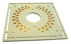
Special PCBs encompass a broad range of applications, each with unique manufacturing challenges. High-frequency PCBs used in telecommunications and radar systems require precise impedance control and minimal signal loss. Flexible PCBs for wearable devices and automotive applications must withstand repeated bending while maintaining electrical integrity. Medical device PCBs demand exceptional reliability and biocompatibility, while aerospace applications require boards that can operate in extreme temperatures and radiation environments.
The substrate materials alone present significant manufacturing complexities. While standard PCBs typically use FR-4 fiberglass, special applications may require polyimide for flexibility, PTFE-based materials for high-frequency performance, or ceramic substrates for thermal management. Each material brings distinct processing requirements, from different etching chemistries to specialized drilling techniques and unique lamination parameters.
Advanced Design for Manufacturing Principles
Optimizing special PCB manufacturing begins at the design stage through comprehensive design for manufacturing (DFM) analysis. This process involves close collaboration between design engineers and manufacturing specialists to identify potential production challenges before they impact yield or quality. For high-frequency applications, this means careful consideration of trace geometry, via placement, and ground plane continuity to maintain signal integrity throughout the manufacturing process.
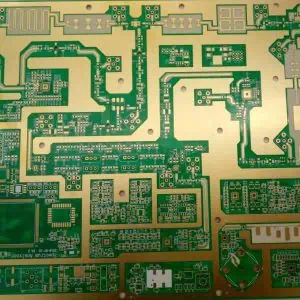
Stackup optimization plays a crucial role in special PCB manufacturing. The arrangement of copper layers, dielectric materials, and their thicknesses must be precisely controlled to achieve desired electrical characteristics while remaining manufacturable. Advanced simulation tools help predict how manufacturing tolerances will affect final performance, allowing designers to build in appropriate margins while minimizing over-engineering.
Material selection optimization extends beyond basic electrical requirements to consider manufacturing compatibility. The coefficient of thermal expansion mismatch between different materials can cause registration issues during lamination, while some high-performance materials may require modified processing temperatures or atmospheres. Successful optimization requires understanding these interactions and designing stackups that achieve performance goals while remaining producible with high yield.
Precision Manufacturing Techniques
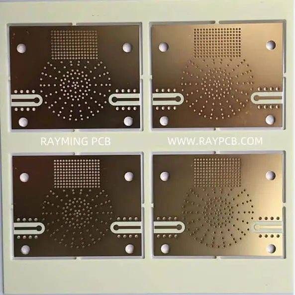
The manufacturing of special PCBs demands precision far beyond standard production capabilities. Drilling operations, for instance, must account for the unique properties of specialized substrates. PTFE-based materials can cause drill bit wandering due to their low friction coefficient, requiring specialized drill bits and modified drilling parameters. Polyimide flexible circuits need carefully controlled entry and exit materials to prevent tearing during drilling operations.
Etching processes for special PCBs often require customized chemistries and parameters. High-frequency boards may use thicker copper to reduce resistance, necessitating longer etch times and more aggressive chemistries that can affect fine-pitch features. Some materials are sensitive to certain etchants, requiring alternative processes or protective measures. The optimization of etch compensation becomes critical when working with mixed dielectrics that etch at different rates.
Lamination represents perhaps the most critical process in special PCB manufacturing. The combination of temperature, pressure, and time must be precisely controlled to achieve proper bonding while avoiding material degradation. Some high-performance materials have narrow processing windows, requiring sophisticated press control systems and careful monitoring. Vacuum lamination may be necessary for certain applications to eliminate voids that could affect electrical performance or reliability.
Quality Control and Testing Optimization
Special PCBs require enhanced quality control measures that go far beyond standard electrical testing. High-frequency boards need specialized test equipment capable of measuring impedance, insertion loss, and other RF parameters across their intended frequency range. This testing must be integrated into the manufacturing flow to catch deviations early, as rework options are often limited with exotic materials.
In-process monitoring becomes crucial for special PCB optimization. Real-time measurement of key parameters during manufacturing allows for immediate correction of drift conditions before they affect product quality. This might include continuous monitoring of etch rates, lamination temperature profiles, or drill registration accuracy. Statistical process control techniques help identify trends that could indicate equipment drift or material variation.
Non-destructive testing methods play an increasingly important role in special PCB manufacturing. Micro-sectioning for traditional cross-sectional analysis can damage expensive boards, making techniques like X-ray inspection, ultrasonic testing, and advanced optical inspection more valuable. These methods can detect internal defects, delamination, or material inconsistencies without compromising the product.
Process Flow Optimization
The manufacturing sequence for special PCBs often differs significantly from standard processes. Flexible circuits may require specialized handling fixtures throughout production to prevent damage from bending or stretching. Rigid-flex boards need careful planning of the fabrication sequence to protect flexible regions during processing of rigid areas.
Optimization of process flow considers the unique requirements of each manufacturing step and their interactions. For example, the thermal history of high-frequency materials can affect their electrical properties, requiring careful sequencing of heat-intensive operations. Some processes may need to be performed in controlled atmospheres to prevent oxidation or contamination of sensitive materials.
Automation plays a crucial role in optimizing special PCB manufacturing, but must be carefully implemented. Standard automation equipment may not be suitable for handling delicate flexible circuits or boards with non-standard thicknesses. Custom fixturing and handling systems are often necessary to maintain process control while protecting sensitive products.
Yield Improvement Strategies
Yield optimization for special PCBs requires a comprehensive approach that addresses both manufacturing defects and design-related issues. Pareto analysis of defect sources helps focus improvement efforts on the most impactful issues. Common challenges include registration problems between layers, material handling damage, and process-induced stress that can cause delamination or cracking.
Statistical analysis of manufacturing data helps identify the optimal process windows for each parameter. Design of experiments (DOE) techniques can efficiently explore the interaction between multiple variables to find optimal settings. This is particularly important for processes with narrow operating windows where small variations can significantly impact yield.
Preventive maintenance programs become even more critical for special PCB manufacturing due to the tight tolerances required. Equipment calibration schedules must account for the precision demands of specialized processes, and predictive maintenance techniques can help avoid unexpected failures that could damage expensive materials or compromise product quality.
Cost Optimization Strategies
While special PCBs inherently carry higher costs than standard products, careful optimization can significantly improve cost-effectiveness. Material utilization optimization through improved panel layouts can reduce waste of expensive substrates. This requires sophisticated nesting algorithms that account for the unique constraints of special materials, such as grain direction in flexible substrates or the location of fiberglass weave patterns.
Process optimization can reduce manufacturing time and improve throughput without compromising quality. This might involve optimizing cure cycles for specialized adhesives, reducing the number of process steps through innovative techniques, or improving equipment utilization through better scheduling algorithms.
Supply chain optimization becomes particularly important for special PCBs due to the specialized nature of materials and equipment. Long lead times for exotic materials require careful inventory management and demand forecasting. Strategic partnerships with suppliers can provide access to technical expertise and ensure priority allocation of limited materials.
Future Trends and Technologies
The optimization of special PCB manufacturing continues to evolve with advancing technology. Additive manufacturing techniques show promise for creating complex three-dimensional circuits that would be impossible with traditional subtractive methods. Digital printing of conductive inks could enable rapid prototyping and small-volume production of specialized circuits.
Artificial intelligence and machine learning are beginning to impact special PCB manufacturing through predictive quality control and process optimization. These technologies can identify subtle patterns in manufacturing data that indicate potential quality issues before they manifest as defects.
Advanced materials continue to push the boundaries of what’s possible in special PCB applications. New dielectric materials with improved properties, embedded components that integrate active devices within the PCB structure, and novel conductor materials all present both opportunities and manufacturing challenges that will require continued process optimization.
The optimization of manufacturing processes for special PCBs represents a continuous journey of improvement, driven by the ever-increasing demands of advanced electronic systems. Success requires a holistic approach that considers design, materials, processes, and quality control as integrated elements of a complex manufacturing system. As technology continues to advance, the ability to efficiently manufacture these specialized products will become an increasingly important competitive advantage in the electronics industry.