Printed Circuit Board (PCB) layout design is a crucial aspect of the product development process, as it directly impacts the manufacturability, performance, and reliability of the final product. Overlooking common design pitfalls can lead to a range of issues, including increased production costs, extended lead times, and even product failures. In this comprehensive guide, we will delve into the most common mistakes to avoid in PCB layout design for enhanced manufacturability.
Importance of Manufacturability in PCB Layout Design
The layout design of a PCB plays a pivotal role in determining its overall manufacturability. A well-designed layout not only ensures the proper functioning of the circuit but also facilitates the efficient and cost-effective production of the board. Conversely, poorly designed layouts can introduce a myriad of challenges during the manufacturing process, resulting in increased scrap rates, yield losses, and higher overall costs.
By understanding and avoiding common design pitfalls, PCB designers can optimize their layouts to meet the requirements of modern manufacturing processes, ultimately delivering high-quality products to their customers in a timely and cost-effective manner.
Common Mistakes to Avoid in PCB Layout Design

To ensure the manufacturability of your PCB, it is essential to be aware of the following common mistakes and how to address them effectively:
1. Insufficient Trace and Space Clearance
Trace and space clearance refer to the distance between adjacent copper traces and the spacing between pads or traces. Inadequate clearance can lead to several manufacturing issues, such as:
- Shorts and Electrical Leakage: Insufficient clearance can result in short circuits or electrical leakage between traces, compromising the performance and reliability of the PCB.
- Difficulty in Etching and Plating: Tight clearances can make it challenging for the manufacturing process to accurately etch and plate the copper layers, leading to defects and yield losses.
- Challenges in Solder Mask Application: Insufficient clearance can complicate the solder mask application process, increasing the risk of solder bridges and other assembly-related issues.
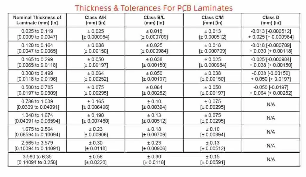
To ensure proper manufacturability, it is recommended to follow the minimum trace and space clearance guidelines provided by the PCB manufacturer or industry standards, such as IPC-2221 or IPC-2222.
2. Improper Via Placement and Design
Vias are essential for connecting different copper layers in a multilayer PCB. However, improper via placement and design can introduce several manufacturing challenges, including:
- Difficulty in Drilling and Plating: Poorly placed vias or vias with unsuitable dimensions can make the drilling and plating processes more challenging, leading to increased defects and reduced yields.
- Reliability Concerns: Vias that are too close to the board edge or other features can compromise the overall structural integrity and reliability of the PCB.
- Impedance Mismatches: Vias with incorrect dimensions or improper placement can cause impedance mismatches, leading to signal integrity issues and potential performance degradation.
To address these challenges, it is crucial to follow the via design guidelines provided by the PCB manufacturer, considering factors such as via diameter, aspect ratio, and placement relative to other board features.
3. Inadequate Copper Weight and Trace Width

The copper weight and trace width of a PCB play a significant role in its manufacturability, electrical performance, and thermal management. Overlooking these design considerations can result in the following issues:
- Difficulty in Etching and Plating: Thick copper layers or wide traces can make the etching and plating processes more challenging, increasing the risk of defects and reducing overall yields.
- Thermal Management Challenges: Insufficient copper weight or narrow trace widths can limit the PCB’s ability to dissipate heat, leading to thermal management issues and potential performance degradation.
- Electrical Performance Concerns: Improper copper weight or trace width can result in impedance mismatches, signal integrity problems, and other electrical performance issues.
To ensure optimal manufacturability and performance, it is essential to select the appropriate copper weight and trace widths based on the specific requirements of the PCB design, considering factors such as current-carrying capacity, thermal management, and electrical performance.
4. Insufficient Solder Mask Clearance
The solder mask is a critical component of the PCB, as it serves to protect the copper traces and prevent short circuits during the assembly process. Inadequate solder mask clearance can lead to the following issues:
- Solder Bridging and Shorts: Insufficient clearance between the solder mask and the copper traces can result in solder bridges and short circuits during the assembly process.
- Difficulty in Solder Mask Application: Tight clearances can make it challenging for the manufacturing process to accurately apply the solder mask, leading to defects and reduced yields.
- Increased Risk of Damage: Insufficient clearance can increase the risk of damage to the solder mask during the manufacturing and assembly processes, compromising the overall reliability of the PCB.
To mitigate these issues, it is recommended to follow the solder mask clearance guidelines provided by the PCB manufacturer or industry standards, such as IPC-2221 or IPC-7351.
5. Improper Silkscreen Placement and Design
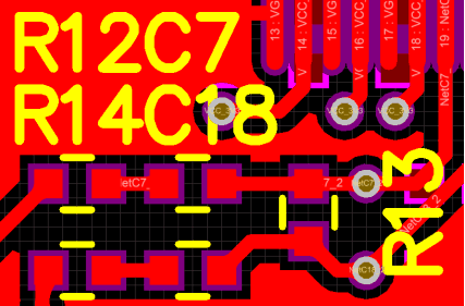
The silkscreen, which includes the component designators, logos, and other surface markings, is an essential element of the PCB layout. Improper silkscreen placement and design can lead to the following challenges:
- Interference with Assembly: Silkscreen elements that overlap with component placement areas or interfere with the assembly process can result in manufacturing issues and potential product failures.
- Reduced Readability: Poorly designed or positioned silkscreen elements can make it difficult for the assembly technicians to identify and orient the components correctly, leading to assembly errors.
- Cosmetic Defects: Improper silkscreen placement or design can result in aesthetic issues, such as overlapping or misaligned markings, which can be undesirable for the end-user.
To ensure optimal manufacturability and usability, it is essential to carefully plan the silkscreen layout, considering the placement of components, assembly processes, and overall readability of the markings.
6. Disregard for Manufacturing Tolerances
Every manufacturing process has inherent tolerances and limitations that must be taken into account during the PCB layout design. Disregarding these tolerances can lead to a range of issues, including:
- Yield Losses: Failing to account for manufacturing tolerances can result in the production of non-conforming boards, leading to increased scrap rates and reduced yields.
- Reliability Concerns: Ignoring manufacturing tolerances can compromise the structural integrity and long-term reliability of the PCB, potentially leading to premature failures in the field.
- Increased Costs: Neglecting manufacturing tolerances can necessitate the use of tighter design rules, which can significantly increase the overall cost of the PCB production.
To address this challenge, it is crucial to closely collaborate with the PCB manufacturer, understand their specific capabilities and tolerances, and design the layout accordingly. This may involve the use of design-for-manufacturing (DFM) tools or seeking guidance from the manufacturer’s technical support team.
7. Lack of Consideration for Test and Inspection Processes
The PCB layout design should also consider the requirements of the test and inspection processes during manufacturing. Overlooking these aspects can lead to the following issues:
- Difficulty in Testing: Poorly designed test points or inaccessible components can make it challenging to effectively test the PCB during the manufacturing process, leading to reduced quality and increased rework.
- Inspection Challenges: Obstructed or hard-to-reach areas on the PCB can make it difficult for the manufacturing team to perform visual inspections, increasing the risk of undetected defects.
- Reliability Concerns: Failure to consider the test and inspection requirements can result in the production of PCBs with hidden defects or reliability issues that may only surface later in the product’s lifecycle.
To address these challenges, it is essential to collaborate with the manufacturing team, understand their test and inspection requirements, and incorporate design elements that facilitate efficient and effective quality assurance processes.
8. Disregard for Component Placement and Orientation
The placement and orientation of components on the PCB can significantly impact the overall manufacturability and assembly process. Ignoring these considerations can lead to the following issues:
- Assembly Difficulties: Poorly placed or oriented components can make the assembly process more challenging, leading to increased errors, rework, and reduced efficiency.
- Interference with Other Components: Improper component placement can result in interference with neighboring components, causing clearance issues and potential performance degradation.
- Thermal Management Concerns: Inadequate spacing or improper placement of heat-generating components can lead to thermal management problems and potential performance issues.
To ensure optimal component placement and orientation, it is essential to consider factors such as component size, heat generation, assembly process requirements, and overall board layout optimization.
9. Lack of Design for Testability (DFT)
Design for Testability (DFT) is a crucial aspect of PCB layout design that ensures the board can be effectively tested and diagnosed during the manufacturing process. Neglecting DFT can result in the following problems:
- Difficulty in Testing: Poorly designed test points or a lack of testability features can make it challenging to thoroughly test the PCB, leading to reduced quality and increased rework.
- Increased Debugging Efforts: Without proper DFT considerations, identifying and resolving issues during the manufacturing process can become more time-consuming and costly.
- Reduced Fault Coverage: Insufficient DFT features can result in lower fault coverage during testing, increasing the risk of undetected defects and potential product failures.
To address these challenges, it is essential to incorporate DFT principles into the PCB layout design, such as strategically placed test points, built-in self-test (BIST) capabilities, and other testability features that facilitate efficient and effective quality assurance.
10. Disregard for Manufacturing Processes and Equipment Capabilities
Each PCB manufacturing facility has its own set of processes, equipment, and capabilities. Failing to consider these factors during the layout design can lead to a range of issues, including:
- Incompatibility with Manufacturing Processes: Designing a layout that is not compatible with the manufacturer’s processes can result in production challenges, increased lead times, and higher costs.
- Limitations of Manufacturing Equipment: Ignoring the capabilities of the manufacturer’s equipment, such as drill bit sizes, plating thickness, or board size limitations, can lead to design-related defects and reduced yields.
- Lack of Design Optimization: Disregarding the manufacturer’s specific capabilities can prevent the designer from optimizing the layout for the most cost-effective and efficient production.
To address this challenge, it is essential to engage with the PCB manufacturer early in the design process, understand their capabilities, and design the layout accordingly. This collaborative approach can help ensure the manufacturability and cost-effectiveness of the final product.
FAQ
Q1: What are the consequences of insufficient trace and space clearance in PCB layout design?
A1: Insufficient trace and space clearance can lead to several manufacturing issues, including:
- Shorts and electrical leakage due to the proximity of traces
- Difficulty in the etching and plating processes, resulting in defects and yield losses
- Challenges in the solder mask application, increasing the risk of solder bridges and other assembly-related issues
To ensure proper manufacturability, it is recommended to follow the minimum trace and space clearance guidelines provided by the PCB manufacturer or industry standards.
Q2: How can improper via placement and design impact the PCB manufacturing process?
A2: Improper via placement and design can introduce several challenges, such as:
- Difficulty in drilling and plating the vias, leading to increased defects and reduced yields
- Reliability concerns due to vias placed too close to the board edge or other features
- Impedance mismatches caused by vias with incorrect dimensions or placement, leading to signal integrity issues
To address these challenges, it is crucial to follow the via design guidelines provided by the PCB manufacturer and consider factors like via diameter, aspect ratio, and placement relative to other board features.
Q3: What are the consequences of inadequate copper weight and trace width in PCB layout design?
A3: Inadequate copper weight or trace width can result in the following issues:
- Difficulty in the etching and plating processes, increasing the risk of defects and reducing overall yields
- Thermal management challenges due to limited heat dissipation capabilities
- Electrical performance concerns, such as impedance mismatches and signal integrity problems
To ensure optimal manufacturability and performance, it is essential to select the appropriate copper weight and trace widths based on the specific requirements of the PCB design.
Q4: How can insufficient solder mask clearance impact the PCB manufacturing process?
A4: Insufficient solder mask clearance can lead to the following issues:
- Solder bridging and shorts during the assembly process due to the proximity of the copper traces
- Difficulty in the solder mask application, resulting in defects and reduced yields
- Increased risk of damage to the solder mask during manufacturing and assembly
To mitigate these issues, it is recommended to follow the solder mask clearance guidelines provided by the PCB manufacturer or industry standards.
Q5: Why is it important to consider manufacturing tolerances during the PCB layout design process?
A5: Disregarding manufacturing tolerances can lead to several problems, including:
- Yield losses due to the production of non-conforming boards
- Reliability concerns as the structural integrity and long-term performance of the PCB may be compromised
- Increased overall costs, as the use of tighter design rules may be necessary to accommodate the manufacturing limitations
To address this challenge, it is crucial to collaborate with the PCB manufacturer, understand their specific capabilities and tolerances, and design the layout accordingly.