In the world of Printed Circuit Board (PCB) design and manufacturing, seamless communication between designers and fabricators is crucial. As the complexity of electronic designs increases, so does the need for more comprehensive and error-free data formats. Enter KiCad’s ODB++ export functionality – a game-changing feature that’s revolutionizing how open-source PCB designs transition from concept to reality. This article delves into the intricacies of KiCad’s ODB++ export, exploring its significance in modern PCB manufacturing workflows and how it’s bridging the gap between design and production.
Introduction
The journey from a PCB design to a physical board involves multiple steps, each critical to the final product’s quality and functionality. Traditionally, this process relied heavily on Gerber files – a long-standing industry standard for communicating PCB design data. However, as designs grow more complex, the limitations of Gerber files become increasingly apparent.
KiCad, a popular open-source electronic design automation (EDA) software, has been at the forefront of addressing these challenges. With its recent introduction of ODB++ export capabilities, KiCad is not just keeping pace with industry trends – it’s setting new standards for open-source PCB design tools.
This article aims to explore how KiCad’s ODB++ export enhances the PCB manufacturing process, offering insights into its implementation, benefits, and best practices for designers and manufacturers alike.
What is ODB++?
Definition and History
ODB++ (Open Database++) is a proprietary PCB manufacturing data exchange format developed by Valor Computerized Systems, now part of Siemens Digital Industries Software. Introduced in the 1990s, ODB++ was designed to address the limitations of traditional Gerber files by providing a more comprehensive and intelligent data format for PCB manufacturing.
Why ODB++ Matters
Unlike traditional Gerber files, which primarily contain 2D image data of PCB layers, ODB++ offers a richer, more complete representation of the PCB design. This comprehensive approach includes:
- Layer information
- Netlist data
- Component placement
- Manufacturing notes
- Material specifications
The result is a single, cohesive package that contains all the information needed to manufacture a PCB, reducing the chances of misinterpretation or data loss between design and production stages.
Key Benefits of ODB++ in PCB Manufacturing
- Fewer Errors: By providing a more complete dataset, ODB++ reduces the likelihood of miscommunication or missing information, leading to fewer manufacturing errors.
- Easier CAM Processing: Computer-Aided Manufacturing (CAM) systems can directly interpret ODB++ data, streamlining the pre-production process and reducing manual intervention.
- Improved Communication: ODB++ facilitates clearer communication between designers and manufacturers, as all relevant information is contained in a single, standardized format.
- Time and Cost Savings: With reduced errors and streamlined processes, ODB++ can lead to faster turnaround times and lower overall production costs.
KiCad’s Evolution Toward Professional Manufacturing Support

Background on KiCad’s Capabilities
KiCad has long been a favorite among hobbyists and professionals alike for its powerful, free, and open-source approach to PCB design. Historically, KiCad has supported standard output formats like Gerber and Excellon drill files, which have been the industry norm for decades.
Challenges with Traditional Gerber + Drill Files
While Gerber files have served the industry well, they come with limitations:
- Multiple Files: A complete Gerber package typically includes separate files for each PCB layer, drill data, and often additional documentation.
- Limited Intelligence: Gerber files essentially describe PCB layers as images, lacking inherent information about connectivity or component properties.
- Potential for Errors: Managing multiple files increases the risk of missing or mismatched data during the handoff to manufacturers.
Growing Demand for ODB++ in Open-Source Workflows
As more professional designers and manufacturers adopt open-source tools like KiCad, the demand for industry-standard outputs like ODB++ has grown. This push reflects a broader trend in the industry towards more integrated, data-rich design-to-manufacturing workflows.
KiCad’s ODB++ Implementation
KiCad introduced ODB++ export capabilities in version 6.0, with continued improvements in subsequent releases. This addition marked a significant step in KiCad’s evolution, aligning it more closely with commercial EDA tools and professional manufacturing requirements.
Read more about:
How KiCad Exports ODB++
Step-by-Step Guide to ODB++ Export in KiCad
- Open Your PCB Project: Ensure your design is finalized and ready for manufacturing.
- Access the Export Menu:
- Navigate to “File” > “Export” > “ODB++”
- Alternatively, use the shortcut Ctrl+Alt+O (Windows/Linux) or Cmd+Alt+O (Mac)
- Configure Export Settings:
- Choose the output directory
- Select layers to include
- Specify netlist and drill file options
- Review and Confirm: Double-check your settings before initiating the export process.
- Export: Click “Export” to generate the ODB++ files.
Overview of Export Options and Settings
- Layers: Select which PCB layers to include in the ODB++ output.
- Netlist: Choose to include detailed netlist information.
- Drill Files: Specify drill file formats and options.
- Component Placement: Include data on component positions and orientations.
- Design Rules: Option to include DRC (Design Rule Check) information.
Practical Tips for Clean ODB++ Export
- Validate Your Design: Run DRC checks before exporting to ensure your design is error-free.
- Use Consistent Units: Ensure all measurements in your design use consistent units to avoid conversion issues.
- Check Layer Stack-up: Verify that your layer stack-up is correctly defined before export.
- Review Component Properties: Ensure all components have correct footprints and attributes assigned.
Common Mistakes to Avoid
- Incomplete Layer Selection: Forgetting to include critical layers in the export.
- Ignoring DRC Errors: Exporting without resolving design rule violations.
- Outdated Libraries: Using old component libraries that may not align with current manufacturing standards.
- Neglecting Mechanical Layers: Forgetting to include important mechanical information like board outlines or assembly notes.
Why Use ODB++ with KiCad?
Advantages over Traditional Gerber Exports
- Consolidated Package: ODB++ provides all necessary manufacturing data in a single, organized structure, reducing the risk of missing files.
- Enhanced Data Intelligence: ODB++ includes detailed information about components, nets, and design rules, enabling more intelligent processing by manufacturers.
- Improved Accuracy: The comprehensive nature of ODB++ data reduces the chance of misinterpretation or errors during the manufacturing process.
- Faster Turnaround: With more complete data upfront, manufacturers can often process ODB++ files more quickly, potentially leading to faster production times.
Better Error Checking and Validation
ODB++ allows for more thorough automated checks at the manufacturing stage, catching potential issues that might be missed with Gerber files alone. This can include:
- Component clearance violations
- Copper-to-edge clearances
- More accurate DFM (Design for Manufacturing) analysis
Reduced Back-and-Forth with PCB Fabricators
The comprehensive nature of ODB++ often results in fewer queries from manufacturers, streamlining the production process. This reduction in communication cycles can lead to:
- Faster time-to-market
- Fewer opportunities for miscommunication
- Reduced overall project stress
Real-World Feedback from Manufacturers
Many PCB manufacturers report preferring ODB++ files for several reasons:
- Ease of Use: ODB++ files are often easier to import and process in modern CAM systems.
- Reduced Pre-Production Time: The completeness of ODB++ data often results in less time spent on pre-production setup and checks.
- Higher Confidence: Manufacturers often express higher confidence in the accuracy of ODB++ data compared to traditional Gerber files.
Limitations and Considerations
ODB++ Export Maturity in KiCad
While KiCad’s ODB++ export functionality is a significant advancement, it’s important to note that it’s still a relatively new feature. As with any software feature, there may be occasional bugs or limitations:
- Ongoing Development: The KiCad team continues to refine and improve ODB++ export capabilities with each release.
- Community Feedback: Users are encouraged to report any issues or inconsistencies they encounter to help improve the feature.
- Version Compatibility: Always check the KiCad release notes for the latest information on ODB++ export capabilities and any known issues.
Compatibility Considerations
While ODB++ is growing in popularity, it’s not universally accepted by all PCB manufacturers:
- Check with Your Manufacturer: Always verify that your chosen PCB fabricator accepts and can process ODB++ files.
- Gerber as Backup: Consider providing both ODB++ and traditional Gerber files to ensure compatibility with a wider range of manufacturers.
- Growing Acceptance: More PCB fabricators are adding ODB++ support, but it’s not yet universal.
When to Stick with Traditional Outputs
There are scenarios where traditional Gerber files might still be preferable:
- Simple Designs: For very simple PCBs, the additional complexity of ODB++ might not offer significant advantages.
- Manufacturer Preference: Some PCB fabricators might still prefer or only accept Gerber files.
- Legacy Systems: If you’re working with older manufacturing systems or processes, Gerber files might be more compatible.
Best Practices for Smooth Handoff to PCB Manufacturers

Checklist for Validating ODB++ Files Before Sending
- Layer Completeness: Ensure all necessary layers are included in the ODB++ package.
- Netlist Verification: Double-check that the netlist in the ODB++ file matches your design intent.
- Component Placement: Verify that all components are correctly placed and oriented.
- Drill File Accuracy: Confirm that all drill data is accurate and complete.
- Design Rule Compliance: Run a final DRC check to ensure all design rules are met.
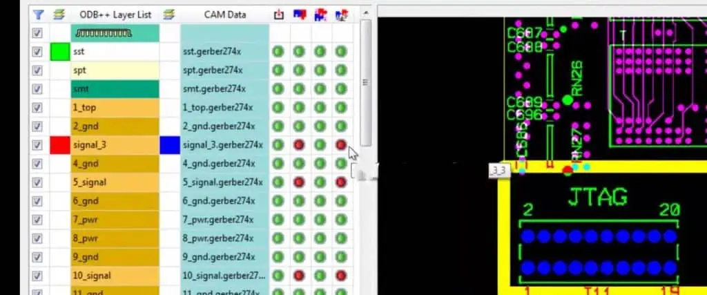
Recommended Tools for Previewing ODB++ Outputs
- ODB++ Viewer: Use specialized ODB++ viewing software to inspect your export.
- CAM350: A professional tool that can open and analyze ODB++ files.
- CircuitCAM: Another professional option for viewing and validating ODB++ data.
- Online Viewers: Some PCB manufacturers offer online tools to preview and check ODB++ files before submission.
Communicating with Your PCB Fab About ODB++ Capabilities
- Early Inquiry: Reach out to your manufacturer early in the design process to discuss their ODB++ capabilities.
- Specification Alignment: Ensure your ODB++ export settings align with your manufacturer’s requirements.
- Version Information: Provide information about the KiCad version used for the export, as this can be helpful for troubleshooting.
- Feedback Loop: Establish a clear channel for feedback from the manufacturer regarding the ODB++ files.
Conclusion
KiCad’s support for ODB++ export represents a significant leap forward in bridging the gap between open-source PCB design and professional manufacturing processes. By providing a more comprehensive and intelligent data format, KiCad is empowering designers to communicate their intentions more clearly and efficiently with manufacturers.
The introduction of ODB++ export in KiCad not only enhances the software’s capabilities but also elevates the entire open-source PCB design ecosystem. It demonstrates that open-source tools can indeed meet and even exceed industry standards, providing professionals with powerful, cost-effective alternatives to proprietary solutions.
As KiCad continues to evolve and refine its ODB++ export functionality, designers are encouraged to explore this feature alongside traditional Gerber exports. The potential benefits in terms of reduced errors, faster turnaround times, and improved communication with manufacturers make it a valuable addition to any PCB designer’s toolkit.
The ongoing development and improvement of features like ODB++ export in KiCad underscore the software’s commitment to providing cutting-edge, professional-grade tools to the open-source community. As more designers adopt these advanced features and provide feedback, we can expect to see even greater strides in the capabilities and reliability of open-source PCB design tools.
In embracing ODB++ export with KiCad, designers are not just improving their own workflows – they’re contributing to a broader shift in the industry towards more open, efficient, and collaborative PCB design and manufacturing processes.
Additional Resources
- KiCad Official Documentation on ODB++ Export
- ODB++ Format Specification
- PCB Fabrication and Assembly Guidelines
FAQ
Does KiCad support ODB++?
Yes, KiCad supports ODB++ export starting from version 6.0, with ongoing improvements in subsequent releases.
What’s the difference between ODB++ and Gerber in KiCad?
While Gerber files primarily contain 2D image data of PCB layers, ODB++ provides a more comprehensive package including netlist data, component placement, and manufacturing notes, all in a single, structured format.
Can you edit ODB++ files exported from KiCad?
ODB++ files are not directly editable like Gerber files. They’re intended as a final output for manufacturing. Any changes should be made in the original KiCad design and then re-exported.