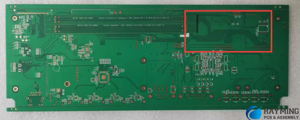
In the ever-evolving world of electronic design, the importance of signal integrity in printed circuit boards (PCBs) cannot be overstated. As clock speeds increase and signal rise times decrease, maintaining signal quality throughout the PCB becomes increasingly challenging. One critical aspect of this challenge is the impedance control of vias – the small plated holes that allow signals to transition between different layers of a multi-layer PCB.
This article delves into the intricate relationship between via impedance control and signal integrity in PCB design. We will explore the fundamentals of impedance, the role of vias in PCB design, various techniques for controlling via impedance, and the profound impact these factors have on overall signal integrity.
Understanding Impedance and Signal Integrity
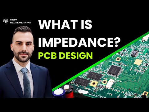
What is Impedance?
Impedance, in the context of electrical circuits, is a measure of the opposition that a circuit presents to the flow of alternating current (AC). It is a complex quantity that includes both resistance and reactance. In PCB design, maintaining consistent impedance throughout signal paths is crucial for ensuring proper signal transmission and minimizing reflections.
Signal Integrity Basics
Signal integrity refers to the quality of an electrical signal as it travels through a PCB. Good signal integrity means that the signal arrives at its destination with minimal distortion, maintaining its original shape and timing characteristics. Factors affecting signal integrity include:
- Impedance mismatches
- Crosstalk
- Electromagnetic interference (EMI)
- Attenuation
- Propagation delay
The Relationship Between Impedance and Signal Integrity
Impedance control is fundamental to maintaining good signal integrity. When a signal encounters an impedance mismatch along its path, part of the signal is reflected back towards the source, causing distortions and potentially leading to errors in data transmission. By carefully controlling impedance throughout the PCB, including in vias, designers can minimize these reflections and maintain signal quality.
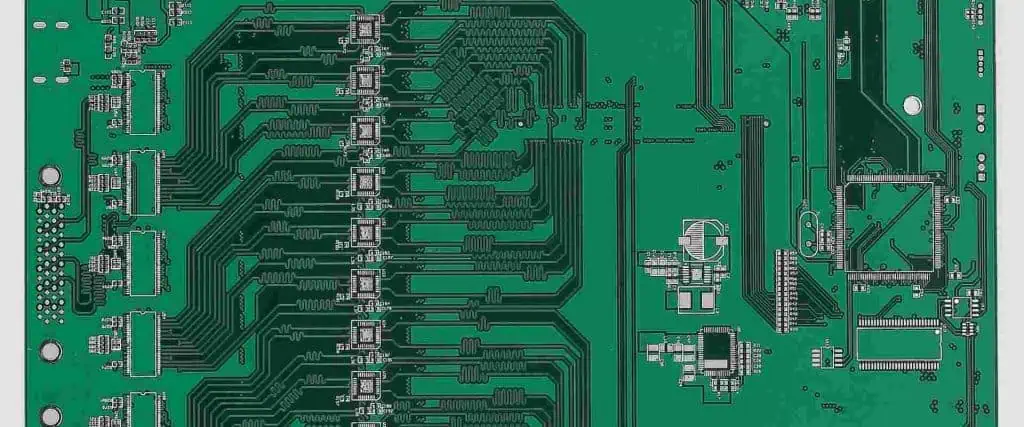
The Role of Vias in PCB Design
Types of Vias
Vias play a crucial role in multi-layer PCB designs, allowing signals to transition between different layers. There are several types of vias:
- Through-hole vias: Extend through all layers of the PCB
- Blind vias: Connect an outer layer to one or more inner layers
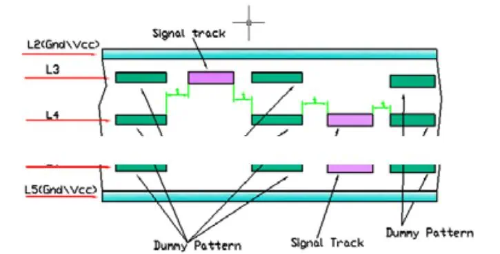
- Buried vias: Connect inner layers without reaching the surface
- Microvia: Very small vias typically used in high-density designs
Via Functions in PCB Design
Vias serve multiple purposes in PCB design:
- Signal routing between layers
- Power and ground connections
- Thermal management
- Component mounting
Challenges Associated with Vias
While vias are essential for multi-layer PCB designs, they also introduce several challenges:
- Impedance discontinuities
- Signal reflections
- Increased crosstalk
- Added capacitance
- Potential for manufacturing defects
Impedance Control Techniques for Vias

Controlling the impedance of vias is crucial for maintaining signal integrity in high-speed PCB designs. Several techniques can be employed to achieve this:
Via Sizing and Geometry
The size and shape of a via can significantly impact its impedance. Key factors include:
- Via diameter
- Pad size
- Antipad size
- Via length (barrel height)
Back-Drilling
Back-drilling involves removing the unused portion of a through-hole via, reducing its length and associated capacitance. This technique is particularly useful for high-speed signals on inner layers.
Via Stitching
Via stitching involves placing multiple vias in parallel to reduce the overall impedance and improve signal quality. This technique is often used for power and ground connections.
Impedance Matching Techniques
Various methods can be used to match the impedance of vias to the surrounding traces:
- Tapered traces leading to vias
- Compensation pads
- Stub removal
Example: Via Impedance Control Parameters
| Parameter | Typical Range | Impact on Impedance |
| Via Diameter | 6-20 mils | Smaller diameter increases impedance |
| Pad Size | 1.5-2x via diameter | Larger pad decreases impedance |
| Antipad Size | 2-3x via diameter | Larger antipad increases impedance |
| Via Length | Depends on board thickness | Longer via increases capacitance |
Impact of Via Impedance on Signal Integrity
The impedance of vias can have a significant impact on overall signal integrity in a PCB design. Some key effects include:
Signal Reflections
Impedance mismatches at vias can cause signal reflections, leading to:
- Ringing and overshoot
- Increased jitter
- Reduced eye diagram opening
Insertion Loss
Vias introduce additional insertion loss to the signal path, which can be particularly problematic for high-frequency signals. Factors contributing to insertion loss in vias include:
- Skin effect in the via barrel
- Dielectric losses
- Radiation losses
Crosstalk
Vias can act as antennas, radiating electromagnetic energy and potentially causing crosstalk with nearby signals. Proper via design and placement can help mitigate this issue.
Return Path Discontinuities
Vias can create discontinuities in the return path for high-frequency signals, leading to increased EMI and signal integrity issues.
Design Considerations for Optimal Via Performance
To ensure optimal via performance and maintain signal integrity, PCB designers should consider the following:
Via Placement Strategies
- Minimize the number of vias in high-speed signal paths
- Place vias as close as possible to the source and load
- Use dedicated ground vias near signal vias to maintain a consistent return path
Stackup Design
The PCB stackup plays a crucial role in via performance:
- Use symmetrical stackups to minimize layer transitions
- Maintain consistent reference planes for each signal layer
- Consider using buried capacitance layers for improved power integrity
Impedance Matching Techniques
- Use tapered traces leading to vias
- Implement compensation pads to match via capacitance
- Consider using stub removal techniques for unused via portions
Signal Routing Best Practices
- Route critical signals on a single layer when possible
- Use differential pairs for high-speed signals
- Maintain consistent trace widths and spacings
Advanced Techniques for Via Impedance Control
As PCB designs become more complex and operating frequencies increase, advanced techniques for via impedance control become necessary:
Coaxial Vias
Coaxial vias use a center conductor surrounded by a ground cylinder, mimicking the structure of a coaxial cable. This design provides excellent impedance control and signal isolation.
Channelized Routing
Channelized routing involves creating dedicated channels for high-speed signals, with ground vias forming walls on either side. This technique helps maintain a consistent return path and reduces crosstalk.
Landless Vias
Landless vias eliminate the pad on layers where the via doesn’t connect, reducing capacitance and improving impedance control.
Via-in-Pad Design
Via-in-pad design places vias directly in component pads, reducing the signal path length and improving performance. This technique requires careful consideration of manufacturing processes to ensure reliable solder joints.
Simulation and Modeling of Via Impedance
Accurate simulation and modeling of via impedance are crucial for optimizing PCB designs:
3D Electromagnetic Simulation
3D electromagnetic simulators can provide detailed insights into via performance, including:
- S-parameters
- Time-domain reflectometry (TDR) responses
- Electric and magnetic field distributions
Equivalent Circuit Models
Simplified equivalent circuit models can be used for rapid analysis of via performance:
- Lumped element models
- Transmission line models
- Hybrid models combining lumped elements and transmission lines
Design of Experiments (DOE) Approach
A DOE approach can be used to systematically explore the impact of various via design parameters on impedance and signal integrity.
Manufacturing Challenges and Solutions
Implementing effective via impedance control in PCB manufacturing presents several challenges:
Drill and Plating Tolerances
Variations in via diameter and plating thickness can affect impedance. Tight control of manufacturing processes is essential.
Material Considerations
The choice of PCB materials can impact via performance:
- Dielectric constant and loss tangent
- Copper foil roughness
- Glass weave effects
High-Aspect-Ratio Vias
Manufacturing high-aspect-ratio vias (small diameter, long length) can be challenging but is often necessary for high-layer-count boards.
Solutions and Best Practices
- Use of laser drilling for small, precise vias
- Implementation of advanced plating techniques
- Careful material selection and specification
- Regular process monitoring and control
Future Trends in Via Design and Impedance Control
As PCB technology continues to evolve, several trends are emerging in via design and impedance control:
Advanced Materials
New PCB materials with improved electrical and thermal properties are being developed, enabling better via performance at high frequencies.
3D Printed Electronics
Additive manufacturing techniques may allow for the creation of custom-shaped vias with optimal impedance characteristics.
Optical Interconnects
As data rates continue to increase, optical interconnects may replace traditional vias for some high-speed applications.
Artificial Intelligence in PCB Design
AI-driven design tools may help optimize via placement and design for improved signal integrity.
Frequently Asked Questions
- Q: How does via impedance affect signal integrity in PCB design? A: Via impedance can significantly impact signal integrity by causing reflections, insertion loss, and crosstalk. Impedance mismatches at vias can lead to signal distortion, increased jitter, and reduced eye diagram opening. Proper impedance control of vias helps maintain signal quality and ensures reliable data transmission in high-speed PCB designs.
- Q: What are the key factors influencing via impedance? A: The main factors influencing via impedance include:
- Via diameter
- Pad and antipad sizes
- Via length (barrel height)
- PCB material properties (dielectric constant, loss tangent)
- Surrounding ground and power planes
- Plating thickness Careful consideration of these factors during design and manufacturing is crucial for achieving the desired via impedance.
- Q: How can I improve via performance in high-speed PCB designs? A: To improve via performance in high-speed PCB designs:
- Minimize the number of vias in critical signal paths
- Use back-drilling to remove unused via stubs
- Implement impedance matching techniques (e.g., tapered traces, compensation pads)
- Consider advanced techniques like coaxial vias or channelized routing
- Use 3D electromagnetic simulation to optimize via design
- Ensure tight manufacturing tolerances for via drilling and plating
- Q: What are the challenges in manufacturing high-performance vias? A: Key challenges in manufacturing high-performance vias include:
- Maintaining tight tolerances for via diameter and plating thickness
- Drilling and plating high-aspect-ratio vias
- Ensuring consistent material properties across the PCB
- Implementing advanced techniques like back-drilling or landless vias
- Balancing performance requirements with manufacturing costs Overcoming these challenges requires close collaboration between PCB designers and manufacturers.
- Q: What future developments can we expect in via design and impedance control? A: Future developments in via design and impedance control may include:
- Advanced PCB materials with improved electrical properties
- 3D printed electronics allowing for custom via shapes
- Integration of optical interconnects for ultra-high-speed applications
- AI-driven design tools for optimizing via placement and performance
- Improved simulation and modeling techniques for more accurate via characterization These advancements will enable PCB designers to create even more efficient and high-performing boards for next-generation electronic devices.