In the world of Printed Circuit Board (PCB) design, one of the most critical aspects is ensuring proper grounding for control power supplies. Grounding defects can lead to a myriad of issues, including electromagnetic interference (EMI), signal integrity problems, and even system failures. This article will explore the concept of defeating control power supply grounding defects through insulation reduction techniques in PCB design.
We will delve into the fundamental principles of grounding, common defects encountered in PCB design, and how insulation reduction can be leveraged to mitigate these issues. By the end of this article, you will have a comprehensive understanding of how to implement effective grounding strategies and optimize your PCB designs for better performance and reliability.

2. Understanding Grounding in PCB Design

2.1 The Importance of Proper Grounding
Grounding is a critical aspect of PCB design that serves several essential functions:
- Providing a reference point for voltage measurements
- Establishing a return path for current flow
- Shielding sensitive components from electromagnetic interference
- Ensuring safety by providing a path for fault currents
2.2 Types of Grounding
There are several types of grounding schemes used in PCB design:
| Grounding Type | Description | Typical Applications |
| Single-Point Grounding | All ground connections converge at a single point | Low-frequency circuits, analog designs |
| Multi-Point Grounding | Multiple ground connections distributed across the board | High-frequency circuits, digital designs |
| Hybrid Grounding | Combination of single-point and multi-point grounding | Mixed-signal designs |
| Floating Ground | Isolated ground plane not connected to earth ground | Battery-powered devices, medical equipment |
2.3 Common Grounding Defects
Despite best efforts, grounding defects can still occur in PCB designs. Some common issues include:
- Ground loops
- Insufficient ground plane coverage
- Poor component placement
- Improper separation of analog and digital grounds
- Inadequate via placement
These defects can lead to various problems, such as increased noise, signal distortion, and reduced system performance.
3. Insulation Reduction Techniques
Insulation reduction is a strategy that can be employed to mitigate grounding defects in PCB design. By strategically reducing insulation in certain areas, we can improve grounding performance and reduce the likelihood of defects.
3.1 Principles of Insulation Reduction
The basic principle behind insulation reduction is to minimize the impedance between different ground points on the PCB. This can be achieved through various techniques:
- Increasing copper pour areas
- Optimizing stackup design
- Strategic via placement
- Implementing ground stitching
- Using buried and blind vias
3.2 Copper Pour Optimization
One of the most effective ways to reduce insulation and improve grounding is through optimized copper pour. This involves:
- Maximizing ground plane coverage
- Minimizing splits in the ground plane
- Using thick copper for power and ground layers
3.3 Stackup Design for Improved Grounding
The PCB stackup can significantly impact grounding performance. Consider the following strategies:
| Layer | Purpose | Benefits |
| Top Layer | Signal routing, component placement | Easy access for components |
| Power Plane | Power distribution | Low impedance power delivery |
| Ground Plane | Return current path | Reduced EMI, improved signal integrity |
| Inner Signal Layers | High-speed signal routing | Shielding from external interference |
| Bottom Layer | Additional routing, ground plane | Improved thermal management |
3.4 Strategic Via Placement
Proper via placement is crucial for effective grounding. Consider these techniques:
- Place vias near high-frequency components
- Use via fencing for improved isolation
- Implement ground vias in a grid pattern for better current distribution
4. Implementing Insulation Reduction in PCB Design

Now that we understand the principles of insulation reduction, let’s explore how to implement these techniques in practice.
4.1 Ground Plane Design
When designing the ground plane, consider the following:
- Use a solid ground plane whenever possible
- Minimize cuts and splits in the ground plane
- Ensure proper ground plane coverage under high-speed signals
- Implement ground islands for sensitive analog circuits
4.2 Component Placement for Optimal Grounding
Proper component placement is crucial for effective grounding:
- Place high-frequency components close to their respective ground connections
- Group similar components together (analog, digital, power)
- Use short and wide traces for power and ground connections
- Implement star grounding for sensitive analog circuits
4.3 Via Stitching Techniques
Via stitching is an effective method for reducing ground impedance:
- Place ground vias along the edges of the board
- Use a grid pattern for ground via placement
- Implement via fencing around high-speed signal traces
- Place vias near decoupling capacitors for improved performance
4.4 Dealing with Mixed-Signal Designs
Mixed-signal designs present unique challenges for grounding. Consider these strategies:
- Separate analog and digital grounds
- Use a split ground plane with a single connection point
- Implement guard traces around sensitive analog signals
- Use dedicated power and ground planes for analog and digital sections
5. Advanced Techniques for Grounding Defect Mitigation
5.1 Electromagnetic Bandgap (EBG) Structures
EBG structures can be used to suppress electromagnetic interference:
- Implement periodic structures in the ground plane
- Use EBG structures to isolate noisy components
- Design custom EBG patterns for specific frequency ranges
5.2 Embedded Capacitance
Embedded capacitance can improve power delivery and reduce ground bounce:
- Use thin dielectric materials between power and ground planes
- Implement embedded capacitance in critical areas of the board
- Combine embedded capacitance with strategic decoupling capacitor placement
5.3 Ground Plane Stitching
Ground plane stitching can help reduce ground impedance in multi-layer designs:
- Use multiple vias to connect ground planes on different layers
- Implement a stitching pattern that follows high-speed signal paths
- Combine ground plane stitching with via fencing for improved isolation
6. Verification and Testing
After implementing insulation reduction techniques, it’s crucial to verify and test the design:
6.1 Simulation and Analysis
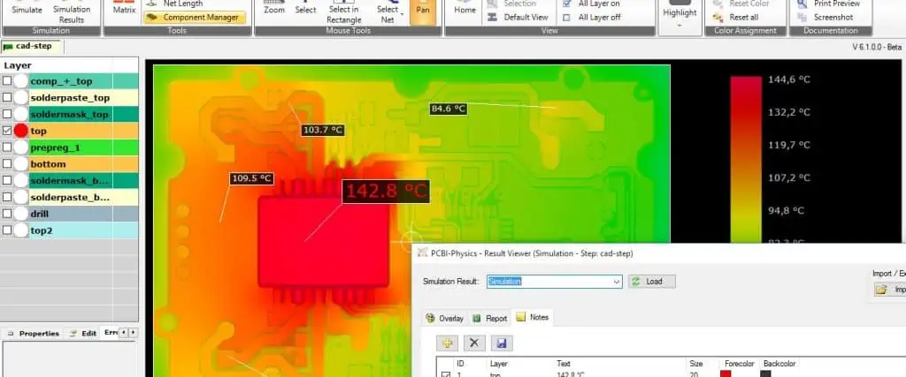
Use electromagnetic simulation tools to:
- Analyze current distribution in the ground plane
- Identify potential EMI hotspots
- Verify signal integrity for critical traces
6.2 Physical Testing
Perform physical tests to ensure proper grounding:
- Use a vector network analyzer to measure impedance
- Conduct EMI/EMC testing to verify compliance with regulations
- Perform functional testing under various operating conditions
7. Case Studies
To illustrate the effectiveness of insulation reduction techniques, consider the following case studies:
7.1 Case Study 1: High-Speed Digital Design
A high-speed digital design experienced signal integrity issues due to grounding defects. By implementing the following insulation reduction techniques, the problems were resolved:
- Optimized stackup with dedicated ground planes
- Implemented via stitching around high-speed traces
- Used embedded capacitance for improved power delivery
Results:
- 40% reduction in EMI emissions
- Improved signal integrity with reduced jitter
- Enhanced overall system performance
7.2 Case Study 2: Mixed-Signal Audio Circuit
A mixed-signal audio circuit suffered from noise and crosstalk issues. The following techniques were applied:
- Separated analog and digital grounds with a single connection point
- Implemented guard traces around sensitive analog signals
- Used a combination of single-point and multi-point grounding
Results:
- 25 dB improvement in signal-to-noise ratio
- Eliminated audible crosstalk between channels
- Achieved compliance with audio equipment standards
8. Conclusion
Defeating control power supply grounding defects through insulation reduction techniques is a crucial aspect of modern PCB design. By implementing the strategies discussed in this article, designers can significantly improve the performance, reliability, and electromagnetic compatibility of their circuits.
Remember that effective grounding is not a one-size-fits-all solution. Each design requires careful consideration of its unique requirements and constraints. Continuously educate yourself on new techniques and technologies to stay at the forefront of PCB design best practices.
9. Frequently Asked Questions (FAQ)
- Q: What is the most common grounding defect in PCB design? A: The most common grounding defect is often ground loops, which occur when there are multiple paths for current to flow back to the source, potentially creating unwanted voltage differences and noise.
- Q: How does insulation reduction help with grounding defects? A: Insulation reduction techniques, such as optimizing copper pours and via placement, help minimize the impedance between different ground points on the PCB. This reduces the likelihood of voltage differences and improves overall grounding performance.
- Q: Can I use a single ground plane for both analog and digital circuits? A: While it’s possible, it’s generally not recommended for sensitive mixed-signal designs. Separating analog and digital grounds with a single connection point (split ground plane) is often a better approach to minimize noise coupling between the two domains.
- Q: How do I determine the optimal number of ground vias to use in my design? A: The optimal number of ground vias depends on factors such as board size, frequency of operation, and current requirements. A general rule of thumb is to place ground vias every quarter-wavelength of the highest frequency of interest, but electromagnetic simulation can provide more accurate guidance for your specific design.
- Q: What are the signs of poor grounding in a PCB design? A: Signs of poor grounding can include excessive EMI emissions, signal integrity issues (such as ringing or reflections), unexpected voltage drops, and system instability. These issues may manifest as intermittent failures, noise in analog signals, or reduced performance in high-speed digital circuits.
