Transient Voltage Suppressor (TVS) diodes have become indispensable components in modern electronic design, serving as the first line of defense against voltage surges and transient events that can devastate sensitive circuitry. These semiconductor devices are ubiquitous across diverse applications, from consumer electronics and medical equipment to industrial automation systems, automotive electronics, and telecommunications infrastructure. Their popularity stems from their exceptional characteristics: lightning-fast response times measured in picoseconds, precise voltage clamping capabilities, and availability in numerous package configurations to suit various design constraints.
In the realm of protection circuit design, the selection of an appropriate TVS diode can mean the difference between robust system reliability and catastrophic failure. However, despite their widespread use, a significant misconception persists among engineers regarding the primary criteria for TVS selection. Many design professionals focus primarily on peak pulse power (PPP) ratings, operating under the assumption that higher power ratings automatically translate to superior protection performance. This oversimplified approach can lead to suboptimal component selection and, in worst-case scenarios, inadequate protection that leaves circuits vulnerable to damage.
Understanding TVS Diode Fundamentals
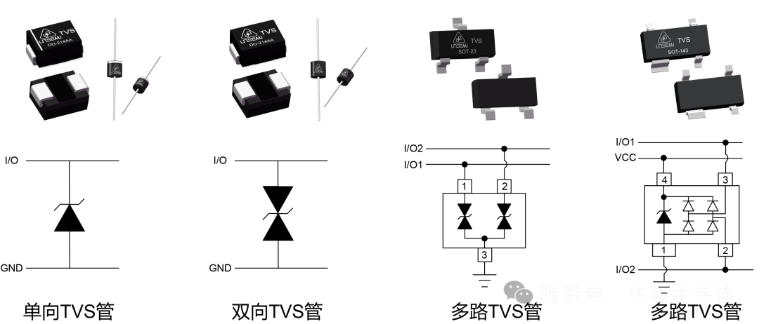
Before delving into selection criteria, it’s essential to understand how TVS diodes function. These devices operate as voltage-controlled switches, remaining in a high-impedance state during normal operation and rapidly transitioning to a low-impedance state when subjected to voltages exceeding their breakdown threshold. This transition effectively clamps the voltage across the protected circuit to a safe level while simultaneously diverting excess current to ground.
The effectiveness of this protection mechanism depends on several critical parameters, each playing a distinct role in the diode’s protective capability. The standoff voltage (VWM) represents the maximum voltage the TVS can withstand without conducting significant current during normal operation. The breakdown voltage (VBR) defines the point at which the device begins to conduct, while the clamping voltage (VC) indicates the actual voltage across the diode when conducting the specified peak current.
The Peak Pulse Power Misconception
The most prevalent myth in TVS diode selection centers on peak pulse power ratings. Many engineers instinctively gravitate toward devices with higher PPP ratings, believing this parameter directly correlates with protection effectiveness. This misconception stems from a fundamental misunderstanding of what PPP actually represents and how it relates to circuit protection.
Peak pulse power rating defines the maximum instantaneous power a TVS diode can handle under specific pulse conditions without sustaining permanent damage. The calculation is straightforward:
PPP = VC × IPP
Where:
- PPP represents the peak pulse power rating
- IPP denotes the peak pulse current flowing through the TVS diode
- VC indicates the clamping voltage across the diode at the specified current level
This relationship reveals a crucial insight: for a given current level, lower clamping voltages result in lower peak pulse power ratings. Counterintuitively, this means the TVS diode with the lowest PPP rating may actually provide the most effective protection.
Real-World Performance Comparison

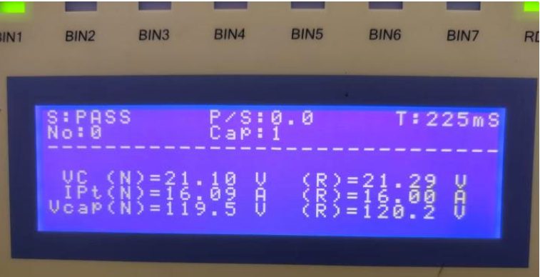
To illustrate this concept, consider three TVS diodes from different manufacturers, all nominally equivalent but exhibiting different performance characteristics under identical test conditions. Using a standardized 10/1000μs pulse waveform at 16A:
Device A: Exhibits a clamping voltage of 15.76V, resulting in PPP = 253.6W Device B: Shows a clamping voltage of 17.28V, yielding PPP = 276.5W
Device C: Demonstrates a clamping voltage of 21.29V, producing PPP = 340.6W
In this scenario, Device A provides the lowest clamping voltage despite having the lowest peak pulse power rating. From a circuit protection standpoint, Device A offers superior performance because it limits the voltage stress on protected components to the lowest level.
The Critical Importance of Clamping Voltage
The clamping voltage represents the actual voltage that protected circuits experience during a transient event. This parameter directly determines whether sensitive components survive the surge or sustain damage. For effective protection, the clamping voltage must remain well below the maximum voltage tolerance of the protected circuitry, providing adequate safety margin for variations in component characteristics and operating conditions.
Consider the voltage tolerances of modern integrated circuits, which often operate with tight margins between normal operating voltages and damage thresholds. A microprocessor designed for 3.3V operation might sustain permanent damage when exposed to voltages exceeding 4V. In such applications, a TVS diode with a 3.8V clamping voltage provides minimal protection margin, while one clamping at 3.5V offers substantially better safety.
Practical Application: Power Supply Protection
To demonstrate proper TVS selection methodology, consider a practical scenario involving a 12V DC/DC converter requiring protection against 1000V surge events per IEC 61000-4-5 standards. The power management IC in this application has a maximum voltage tolerance of 28V, beyond which permanent damage occurs.
The surge testing standard specifies a 2Ω source impedance, allowing calculation of the required peak current handling capability:
IPP = VSurge / RSource = 1000V / 2Ω = 500A
Three TVS candidates all meet the 500A current requirement but differ significantly in their clamping performance:
Option 1: Clamping voltage of 25V at 500A (PPP = 12.5kW) Option 2: Clamping voltage of 28V at 500A (PPP = 14kW) Option 3: Clamping voltage of 30V at 500A (PPP = 15kW)
Applying the common misconception of selecting the highest PPP device would lead to choosing Option 3. However, this choice would result in circuit failure, as the 30V clamping voltage exceeds the IC’s 28V tolerance.
Option 2, while meeting the voltage requirement exactly, provides no safety margin for component variations or multiple stress conditions. Option 1, despite having the lowest PPP rating, represents the optimal choice by providing 3V of protective margin while easily handling the required surge current.
Advanced Selection Considerations
Beyond the fundamental clamping voltage requirement, several additional factors influence TVS selection effectiveness. Process variations in semiconductor manufacturing can cause significant parameter variations between individual devices, even within the same part number. Quality manufacturers typically specify worst-case clamping voltages that account for these variations, but designers must verify that adequate margins exist under all operating conditions.
Temperature effects also play a crucial role in TVS performance. Clamping voltages typically exhibit positive temperature coefficients, meaning they increase with rising temperature. In applications with wide operating temperature ranges or significant self-heating, this effect must be factored into the margin calculations.
The pulse characteristics of expected transient events also influence selection criteria. While standardized test conditions provide baseline comparisons, real-world transients may exhibit different rise times, pulse widths, or repetition rates. TVS diodes optimized for specific pulse characteristics may offer superior protection compared to those selected based solely on standard test conditions.
Multi-Parameter Optimization

Effective TVS selection requires balancing multiple parameters simultaneously. The standoff voltage must exceed normal operating voltages with sufficient margin to prevent false triggering during normal operation. The breakdown voltage should be low enough to ensure prompt response to transient events while remaining above the standoff voltage requirement.
Capacitance considerations become critical in high-frequency applications, where excessive TVS capacitance can degrade signal integrity or reduce system bandwidth. In such cases, designers may need to accept slightly higher clamping voltages in exchange for lower capacitance, requiring careful analysis of the protection versus performance tradeoffs.
Package considerations also influence selection, particularly in space-constrained applications or those with specific thermal management requirements. Surface-mount packages offer compact solutions but may have limited power dissipation capabilities compared to through-hole alternatives.
Industry Standards and Testing Methodologies
Understanding relevant industry standards helps ensure proper TVS selection and application. Standards such as IEC 61000-4-2 (ESD), IEC 61000-4-4 (EFT), and IEC 61000-4-5 (surge) define specific test conditions and performance requirements for different transient threats. Each standard specifies different pulse characteristics, requiring careful analysis to ensure the selected TVS performs adequately across all applicable tests.
Testing methodologies also vary between manufacturers, making direct comparisons challenging. Some suppliers provide extensive characterization data across multiple pulse conditions, while others limit specifications to single test points. Designers should prioritize suppliers offering comprehensive data that enables thorough analysis of protection performance.
Conclusion and Best Practices
The selection of TVS diodes demands a comprehensive understanding of protection requirements and device characteristics that extends far beyond simple peak pulse power comparisons. Effective protection circuit design prioritizes clamping voltage performance while ensuring adequate current handling capability and maintaining appropriate margins for component variations and environmental conditions.
Engineers should develop systematic selection methodologies that evaluate all relevant parameters in the context of specific application requirements. This includes thorough analysis of protected circuit voltage tolerances, expected transient characteristics, operating environment conditions, and applicable regulatory standards.
By abandoning the misconception that higher peak pulse power ratings automatically provide better protection, designers can make informed selections that deliver robust, reliable transient protection while optimizing system performance and cost effectiveness. The key lies in understanding that the primary function of a TVS diode is voltage limitation, not power absorption, and selecting devices accordingly will result in superior protection circuit designs.