In the realm of high-speed printed circuit board (PCB) design, power integrity is a critical factor that can make or break the performance of electronic devices. As clock speeds increase and components become more power-hungry, the need for effective impedance control in PCB power distribution networks (PDNs) becomes paramount. This comprehensive guide delves into the intricacies of analyzing and prohibiting impedance in high-speed PCB power systems, providing engineers and designers with the knowledge and tools necessary to create robust and efficient power delivery solutions.

Understanding Impedance in High-Speed PCB Power
Impedance in PCB power systems refers to the opposition that a circuit presents to the flow of electrical current when a voltage is applied. In high-speed designs, impedance becomes a complex quantity that varies with frequency and consists of both resistive and reactive components.
Components of Impedance
- Resistance (R): The real part of impedance, representing the opposition to DC current flow.
- Inductance (L): The imaginary part of impedance that opposes changes in current flow.
- Capacitance (C): The imaginary part of impedance that opposes changes in voltage.
The total impedance (Z) is given by the formula:
Z = R + j(ωL – 1/ωC)
Where:
- ω is the angular frequency (2πf)
- j is the imaginary unit
Importance of Impedance Control

Controlling impedance in high-speed PCB power systems is crucial for several reasons:
- Voltage Stability: Minimize voltage fluctuations at IC power pins.
- Signal Integrity: Reduce noise and maintain clean signal transitions.
- EMI Reduction: Minimize electromagnetic interference and improve EMC compliance.
- Power Efficiency: Optimize power delivery and reduce losses.
- Thermal Management: Reduce hotspots and improve overall thermal performance.
Factors Affecting PCB Power Impedance
Several factors contribute to the impedance characteristics of a PCB power system:
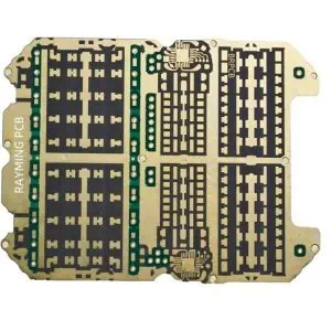
- PCB Stack-up: Layer count, thickness, and material properties.
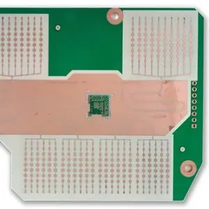
- Power Plane Design: Size, shape, and spacing of power and ground planes.
- Via Design: Size, placement, and density of power and ground vias.
- Decoupling Strategy: Selection and placement of decoupling capacitors.
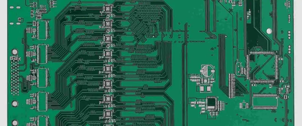
- Trace Geometry: Width, length, and spacing of power traces.
- Component Placement: Proximity of ICs to power sources and decoupling components.
- Frequency: Operating frequencies of the circuits and their harmonics.
Analyzing PCB Power Impedance
Effective impedance analysis involves a combination of theoretical calculations, simulations, and measurements. The goal is to create a comprehensive model of the power distribution network that accurately predicts its behavior across a wide range of frequencies.
Steps in Impedance Analysis
- Define Requirements: Establish target impedance based on IC specifications and system requirements.
- Create PDN Model: Develop an equivalent circuit model of the power distribution network.
- Perform Simulations: Use specialized software to simulate PDN behavior.
- Analyze Results: Examine impedance profiles, voltage ripple, and current distribution.
- Optimize Design: Iteratively refine the design to meet target impedance goals.
- Validate: Perform measurements on prototype boards to verify simulation results.
Tools and Techniques for Impedance Analysis
Several tools and techniques are available for analyzing PCB power impedance:
| Tool/Technique | Description | Advantages | Limitations |
| SPICE Simulation | Circuit-level simulation of PDN | Detailed component-level analysis | Can be computationally intensive for large designs |
| 2D/3D EM Simulation | Electromagnetic field simulation | Accurate modeling of complex geometries | Requires significant computational resources |
| VNA Measurements | Vector Network Analyzer for S-parameter measurements | Provides real-world data | Requires specialized equipment and careful setup |
| TDR Measurements | Time Domain Reflectometry for impedance profiling | Can identify specific locations of impedance discontinuities | Limited frequency range compared to VNA |
| Impedance Analyzer | Dedicated instrument for impedance measurements | High accurac |
Impedance Calculation Methods
Several methods can be used to calculate PCB power impedance:
1. Transmission Line Theory
For simple geometries, transmission line theory can provide quick estimates of characteristic impedance:
Z₀ = √(L/C)
Where:
- Z₀ is the characteristic impedance
- L is the inductance per unit length
- C is the capacitance per unit length
2. Cavity Model
The cavity model is useful for analyzing parallel plate structures:
Z = j2πfL(1 – (f/f₀)²)
Where:
- f is the frequency of interest
- f₀ is the resonant frequency of the cavity
- L is the inductance of the cavity
3. Numerical Methods
For complex geometries, numerical methods such as the Finite Element Method (FEM) or Method of Moments (MoM) are employed in electromagnetic simulation software.
Strategies to Prohibit Unwanted Impedance

Controlling and minimizing unwanted impedance in high-speed PCB power systems involves several strategies:
- Proper PCB Stack-up Design: Optimize layer arrangement and thicknesses.
- Effective Power Plane Design: Implement low-impedance power planes.
- Decoupling Capacitor Optimization: Select and place decoupling capacitors strategically.
- Via Stitching: Use multiple vias to reduce inductance.
- Transmission Line Techniques: Implement controlled impedance power traces where necessary.
- Ground Plane Optimization: Ensure solid, low-impedance return paths.
- EMI Mitigation Techniques: Implement guard traces and shielding where appropriate.
Power Plane Design Considerations
Effective power plane design is crucial for minimizing impedance in high-speed PCB power systems:
- Plane Spacing: Minimize the distance between power and ground planes to increase interplane capacitance.
- Plane Shape: Avoid narrow sections or slots that can create high-impedance paths.
- Plane Pairing: Dedicate adjacent layers to power and ground planes for optimal performance.
- Edge Termination: Implement proper edge termination to minimize reflections.
Recommended Plane Spacing
| Frequency Range | Recommended Plane Spacing |
| < 100 MHz | 10-20 mils |
| 100 MHz – 1 GHz | 4-8 mils |
| > 1 GHz | 2-4 mils |
Decoupling and Bypass Capacitors
Proper selection and placement of decoupling capacitors are essential for controlling impedance:
- Capacitor Selection: Choose capacitors with appropriate values and self-resonant frequencies.
- Placement Strategy: Place capacitors close to IC power pins to minimize loop inductance.
- Parallel Combination: Use multiple capacitors in parallel to cover a wide frequency range.
- Via Proximity: Minimize the distance between capacitor pads and connecting vias.
Typical Decoupling Capacitor Values
| Frequency Range | Recommended Capacitor Values |
| < 1 MHz | 10 µF – 100 µF |
| 1 MHz – 100 MHz | 100 nF – 1 µF |
| 100 MHz – 1 GHz | 1 nF – 10 nF |
| > 1 GHz | 10 pF – 100 pF |
Transmission Line Considerations
In high-speed designs, power traces may need to be treated as transmission lines:
- Impedance Matching: Match trace impedance to source and load impedances.
- Trace Geometry: Control trace width and spacing to achieve desired impedance.
- Return Path: Ensure a clear and low-impedance return path for current.
- Length Matching: Match lengths of differential power traces to minimize skew.
Via Design and Placement
Proper via design and placement are crucial for minimizing impedance in power delivery:
- Via Size: Use larger vias for power connections to reduce inductance.
- Via Placement: Place vias close to IC power pins and decoupling capacitors.
- Via Stitching: Use multiple vias in parallel to reduce overall inductance.
- Back-Drilling: Consider back-drilling vias to reduce stub effects at high frequencies.
Recommended Via Sizes for Power Connections
| Current Rating | Recommended Via Size (Drill Diameter) |
| < 1A | 10 mils |
| 1A – 2A | 13 mils |
| 2A – 3A | 16 mils |
| > 3A | 20 mils or larger |
Ground Plane Optimization
Optimizing ground planes is essential for creating low-impedance return paths:
- Solid Ground Planes: Avoid splits or cuts in ground planes.
- Ground Plane Continuity: Ensure uninterrupted ground planes across the entire board.
- Ground Vias: Use abundant ground vias to minimize return path inductance.
- Ground Plane Spacing: Minimize distance between signal layers and their reference ground planes.
Signal Integrity Considerations
While focusing on power integrity, it’s crucial to consider signal integrity aspects:
- Crosstalk Mitigation: Proper spacing and shielding between power and signal traces.
- Impedance Matching: Ensure power trace impedance matches driver and receiver impedances.
- Reflection Control: Implement proper termination strategies to minimize reflections.
- Jitter Management: Minimize power supply induced jitter through effective decoupling.
EMI and EMC Considerations
Effective impedance control contributes to improved electromagnetic compatibility:
- Edge Rates: Control signal edge rates to minimize high-frequency emissions.
- Shielding: Implement proper shielding techniques for sensitive circuits.
- Filter Design: Incorporate EMI filters in power entry and exit points.
- Current Loop Area: Minimize current loop areas to reduce radiated emissions.
Thermal Management and Impedance
Thermal considerations are intertwined with impedance control:
- Copper Weight: Balance between increased copper for thermal management and impedance control.
- Thermal Vias: Design thermal vias to minimize impact on power plane impedance.
- Component Placement: Consider thermal impacts when placing power components.
- Material Selection: Choose PCB materials with appropriate thermal and electrical properties.
Case Studies: Successful Impedance Control
Case Study 1: High-Speed Memory Interface
Problem: Voltage fluctuations causing data errors in DDR4 memory interface. Solution: Implemented optimized PDN with carefully selected decoupling capacitors and via stitching. Result: 50% reduction in power supply noise, eliminating data errors.
Case Study 2: Mixed-Signal Board with Sensitive Analog Circuits
Problem: Digital switching noise coupling into analog sections. Solution: Implemented split power planes with optimized bridge capacitors and guard traces. Result: 30 dB improvement in noise isolation between digital and analog sections.
Future Trends in High-Speed PCB Power Design
As technology advances, several trends are shaping the future of high-speed PCB power design:
- 3D Power Delivery: Exploring vertical integration of power delivery networks.
- Advanced Materials: Development of new PCB materials with improved electrical and thermal properties.
- Artificial Intelligence in Design: AI-assisted optimization of PDN layouts and component selection.
- Integrated Voltage Regulators: Increased adoption of on-die and package-integrated voltage regulators.
- Higher Frequency Operation: Pushing designs into mmWave frequencies, requiring novel PDN approaches.
Frequently Asked Questions
1. What is the target impedance for a typical high-speed PCB power system?
The target impedance depends on the specific requirements of the ICs and the overall system. A common rule of thumb is to aim for a PDN impedance that is 1/10th of the lowest impedance of any IC on the board. For example, if the lowest IC impedance is 1 ohm, the target PDN impedance would be 0.1 ohm or less across the frequency range of interest.
2. How do I determine the optimal number and placement of decoupling capacitors?
Determining the optimal number and placement of decoupling capacitors involves several steps:
- Analyze the power requirements of each IC, including current draw and frequency content.
- Calculate the target impedance for each power rail.
- Use simulation tools to model the PDN and iteratively add capacitors until the target impedance is met across the frequency range of interest.
- Place capacitors as close as possible to IC power pins, using multiple smaller values in parallel to cover a wide frequency range.
- Validate the design through measurement on prototype boards.
3. What are the key differences in impedance control for digital vs. analog circuits?
Impedance control for digital and analog circuits has some key differences:
Digital Circuits:
- Focus on maintaining low impedance across a wide frequency range
- Emphasis on minimizing switching noise and maintaining voltage stability
- Often use parallel combinations of capacitors to address various frequency components
Analog Circuits:
- More sensitive to noise and require careful isolation from digital sections
- May require separate power planes with optimized filtering
- Often use series inductors in addition to capacitors for better noise rejection
- May need special attention to ground loops and return current paths
4. How does PCB material selection impact power impedance?
PCB material selection can significantly impact power impedance:
- Dielectric Constant (Dk): Materials with lower Dk can reduce parasitic capacitance, potentially lowering impedance at high frequencies.
- Dissipation Factor (Df): Lower Df materials reduce signal loss, which can help maintain lower impedance over longer distances.
- Thermal Conductivity: Better thermal conductivity can help manage heat in power delivery components, indirectly affecting impedance stability.
- Copper Roughness: Smoother copper surfaces can reduce skin effect losses at high frequencies, helping to maintain lower impedance.