Before diving into the specifics of the first circuit board ever made, it’s helpful to understand the history leading up to their invention.
Circuit boards are the foundation of most modern electronics. They allow components like integrated circuits, resistors, capacitors, and more to be interconnected in a structured way. This enables signals to pass between components so complex circuits can be built.
But this wasn’t always the case. In the early days of electronics, all connections had to be made manually by soldering components together with wires. This was a slow, tedious, and error-prone process. It severely limited how complex circuits could become.
Printed circuit boards (PCBs) changed all of this by allowing components to be systematically arranged and pre-connected on a flat surface. This paved the way for electronics to become exponentially more advanced in the 20th century.
So who invented the first circuit board that made this revolution possible?
The Birth of the Circuit Board
The earliest predecessor of the circuit board was invented in 1903 by Albert Hanson, an employee at a German electrical engineering firm called AEG Telegraphy.
His creation consisted of thin strips of insulating tape onto which electrical wiring was pressed by a hot iron. While revolutionary for the time, it lacked many properties of modern PCBs.
The first true printed circuit board is widely credited to have been invented in 1925 by Austrian engineer Paul Eisler. Working in England at the time, he filed a patent for a method of printing electrical circuits onto an insulating baseplate.
His initial prototypes were made using a conductive ink printed onto bakelite sheets. Later he improved the process by using photolithographic etching similar to techniques still used today. This allowed much finer details than his original method.
So Paul Eisler’s circuit boards were the first that resembled modern PCBs as we know them. But they were still manufactured individually by hand.
The Transition to Mass Production
During World War II, the United States military began employing crude printed circuits in proximity fuzes for rockets to increase reliability.
This application demonstrated the usefulness of such technology for the first time on an industrial scale. It paved the way for the techniques developed by Eisler and others to be re-evaluated for mass production rather than one-off prototypes .
In 1947, the United States Army Signal Corps developed the first industrially mass-produced printed circuits at their laboratory at Fort Monmouth, New Jersey.
Engineers automated the photolithographic process developed earlier by Eisler so that sheets of circuits could be reliably reproduced without manual intervention. This transitioned printed circuits from a niche technology to one ready for widespread adoption.
The capabilities of circuits were still limited, however, by relying on individual discrete components soldered to the boards. Jack Kilby invented the integrated circuit in 1958, allowing entire circuits to be miniaturized onto single semiconductor chips. This led to another revolution in capability that married perfectly with printed circuit board technology.
So while Paul Eisler invented the first true circuit board, engineers at Fort Monmouth expanded on his work to enable mass production. And the capabilities of such boards were propelled forward tremendously by the later invention of the integrated circuit.
The First Circuit Boards
Now that we’ve covered a brief history leading up to their invention, what exactly did those first circuit boards made at Fort Monmouth in 1947 look like and what were they capable of?
They were quite primitive by today’s standards but revolutionary for the era. These were some key attributes:
- Base Material: Paper-based phenolic resin
- Maximum Dimensions: Approximately 3 x 5 inches
- Copper Layer Thickness: 1 ounce (35 μm)
- Minimum Spacing Between Lines: ~100 μm
- One-sided with through-hole components
- Reliably mass-producible via photolithography
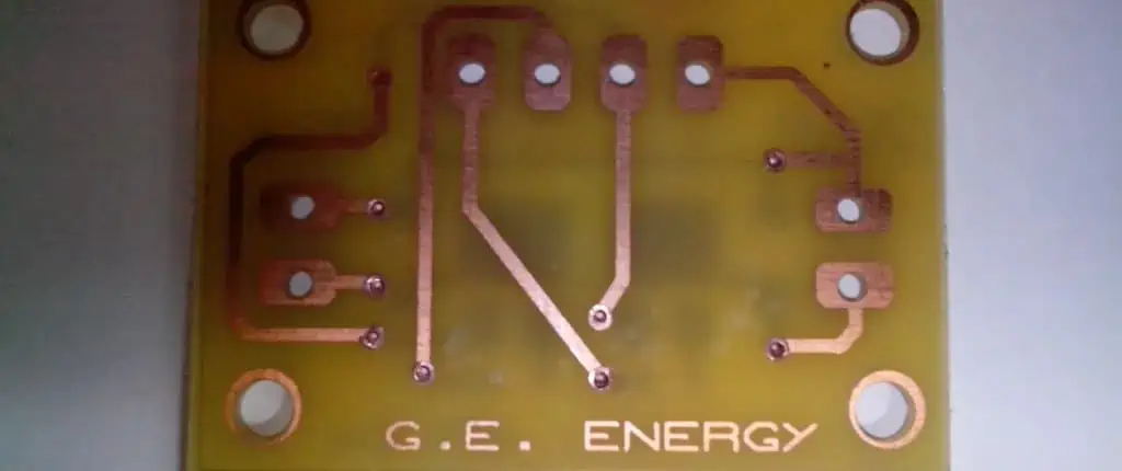
The boards were initially one-sided with tracks on only one outer layer. Holes were drilled or punched into the board so component leads could pass through and be soldered on the opposite side. This “through-hole” design was necessary since surface-mount technology had not yet been invented.
While the capabilities of the initial circuit boards were modest, they led to rapid development once adopted widely. By the early 1950s, double-sided boards with plated through holes became common, greatly increasing circuit complexity.
And surface mount assembly eliminated the need for through-hole components, allowing further miniaturization. So while humble in origin, printed circuit boards enabled an electronics revolution once mass production methods were developed.
Early Single-Layer Circuit Board Capabilities
To visualize the humble beginnings of PCB technology, here are some key specs on those initial one-sided, paper-based boards first mass produced at Fort Monmouth in 1947:
| Property | Capability |
|---|---|
| Dimensions | Up to 3 x 5 inches |
| Copper Thickness | 1 ounce (35 μm) |
| Minimum Spacing | ~100 μm |
| Layers | 1 conductive layer |
| Maximum Components | ~15-30 components |
| Component Types | Through-hole parts |
| Materials | Paper phenolic |
| Frequency | <1 MHz |
Table: Specifications of some of the earliest single-layer printed circuit boards.
While the first circuit boards were modest by today’s standards where boards with 12+ layers are common, they represented a tremendous leap forward in electronics manufacturing at the time. This paved the way for rapid advancements in capability in the coming decades.
Driving Adoption Through Military and Space Applications
Following their initial development at Fort Monmouth in 1947, printed circuit boards quickly gained adoption in American military applications during the 1950s.
Use of PCBs aligned nicely with military goals to miniaturize electronics as much as possible for applications including but not limited to:
- Missile guidance systems
- Airborne radar systems
- Communication radios
Their ability to reliably interconnect miniaturized discrete components in a structured way facilitated this downsizing trend. And as integrated circuits emerged later around 1960, the advantages grew tremendously.
The American space program, which was largely driven by military-trained engineers, brought further demand for printed circuits. In particular, their reliability and resistance to vibration and mechanical stresses fit the needs of space flight.
Throughout the Cold War decades, PCB advancement ran hand-in-hand with military and space objectives, bankrolling continued progress. Commercial applications followed later once initially prohibitively high costs came down.
This military/aerospace lead nurtured PCBs through their infancy until economics expanded their reach more broadly in the 1960s and beyond.
The explosion of commercial PCB applications
By 1965, the manufacture of printed circuit boards in the USA exceeded $1 billion dollars (over $8 billion today). [11] No longer just a niche military product, they now served many commercial applications including:
- Television sets
- Radios
- Business computers
- Control systems
- Test and measurement equipment
And demand further accelerated through the late 1970s as new applications arose including:
- Personal computers
- Video game consoles
- Handheld calculators
- Home appliances
As printed circuits facilitated automated assembly, manufacturing costs fell low enough for broad consumer product adoption. And multi-layer boards drove up interconnect capabilities to support increasingly complex circuitry.
So over just two decades following their invention, PCBs transitioned from narrow military applications to a backbone enabling the electronics industry as we know it today. And capabilities continues to grow according to Moore’s Law thanks to perpetual advancement.
Modern Circuit Boards
Printed circuit board technology has continued advancing rapidly since those initial single-sided versions first mass produced around 1950. Here is a comparison:
| Property | Early 1950s | Today |
|---|---|---|
| Dimensions | 3 x 5 inches | 24 x 24 inches+ |
| Layers | 1-2 conductive layers | 12+ conductive layers |
| Minimum Spacing | ~100 μm | under 50 μm |
| Materials | Paper phenolic | Ceramic, FR-4 fiberglass |
| Frequency | <1 MHz | Multi-GHz |
| Components | 10s per board | 1,000s per board |
Table: Comparison between capabilities of early 1950s printed circuit boards vs. modern boards.
So in the 70+ years since their invention, PCB capabilities across factors like layer counts, component density, operating frequencies and more have increased by orders of magnitude. Driving this progress is a combination of:
- Electronic design automation (EDA) software
- Progress in manufacturing techniques
- Advances in materials science
- Higher purity materials
- Economies of scale
And the electronics revolution enabled by printed circuits shows no sign of slowing down. So while humble in origin, the first circuit boards seeded technology that continues rapidly evolving today.
Frequently Asked Questions
Who invented the first printed circuit board?
The first true printed circuit board resembling modern technology is widely credited to have been invented in 1925 by Austrian engineer Paul Eisler. He filed a patent for a method of printing electrical circuits onto an insulating baseplate using conductive inks and photolithography.
How were early printed circuits mass produced?
Building on Paul Eisler’s work, engineers at Fort Monmouth, New Jersey developed the first photolithographic processes suitable for industrial mass production of printed circuits in 1947. This transitioned them from a niche technology to one ready for widespread adoption.
What materials were early PCBs made from?
Initially paper-based phenolic resin laminates which provided adequate insulation and mechanical stability but were limited in performance compared to later fiberglass-based materials. In the 1950s, FR-4 fiberglass quickly emerged as an improved base material.
How did early PCB capabilities compare to today’s?
Extremely primitive! Those first mass produced boards around 1950 were one-sided with simple through-hole components and dimensions under 5 inches. Today we have enormous boards with 12+ copper layers capable of holding thousands of tiny surface mount components.
How did early adoption of PCBs align with military objectives?
The American military drove early PCB development starting in WWII to achieve electronics miniaturization, reliability and vibration resistance needed for missile guidance and other applications. This nurtured advancement through the critical early stages until costs fell sufficiently for broader commercial adoption.
And that covers some key points on early printed circuit board history – from their origins in Paul Eisler’s 1925 patent to how the technology became revolutionized by mass production methods a few decades later. Let me know if you have any other questions!