Introduction
The ESP32, a powerful and versatile microcontroller, has become a cornerstone in the world of Internet of Things (IoT), embedded systems, and DIY projects. Its popularity stems from its robust Wi-Fi and Bluetooth capabilities, coupled with an impressive array of peripherals and processing power. However, to fully harness the potential of this remarkable chip, proper ESP32 PCB design is crucial.
In this comprehensive guide, we’ll delve into the best practices for ESP32 PCB design, focusing on power management, layout techniques, and ensuring signal integrity. Whether you’re using popular design tools like EasyEDA for ESP32 or Altium Designer for ESP32, these principles will help you create more efficient, reliable, and high-performing ESP32-based devices.
1. Understanding ESP32 Hardware for PCB Design
ESP32 Architecture Overview
Before diving into PCB design, it’s essential to understand the ESP32’s architecture:
- Dual-core Xtensa LX6 CPU
- Integrated Wi-Fi and Bluetooth controllers
- Rich set of GPIOs
- Advanced power management features
Key Considerations for ESP32 Circuit Design
When embarking on an ESP32 PCB design project, keep these factors in mind:
- Power requirements and management
- RF considerations for Wi-Fi and Bluetooth
- GPIO allocation and functionality
- Thermal management
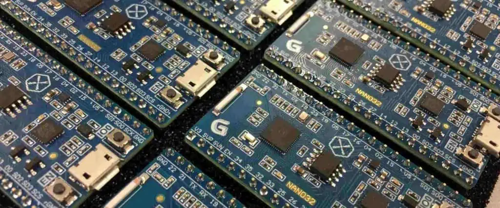
Common ESP32 Modules and Their PCB Implications
Different ESP32 modules have unique PCB design requirements:
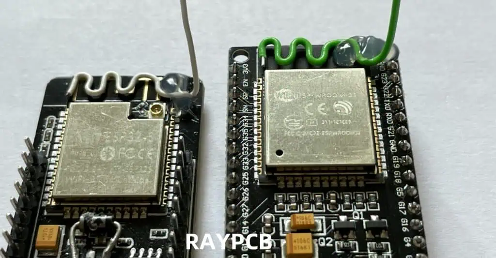
- ESP32-WROOM-32: Requires careful antenna placement and ground plane design
- ESP32-CAM: Needs special considerations for camera module and SD card interfaces
2. Choosing the Right PCB Design Software for ESP32
Comparison of Popular Options
EasyEDA ESP32 Workflow
- Pros: User-friendly interface, cloud-based, free for basic use
- Cons: Limited advanced features compared to professional tools
- Best for: Beginners, hobbyists, and rapid prototyping
Altium Designer ESP32 Advanced Features
- Pros: Comprehensive design environment, advanced routing capabilities, powerful simulation tools
- Cons: Steep learning curve, higher cost
- Best for: Professional designers, complex ESP32 projects
Tips for Transferring ESP32 Schematic to PCB Layout
- Use hierarchical design for complex ESP32 circuits
- Leverage cross-probing between schematic and PCB
- Utilize design reuse features for common ESP32 subcircuits
Read more about:
3. Power Supply Design Best Practices
Importance of Clean Power in ESP32 PCB Design
A stable and clean power supply is critical for ESP32 performance, especially for sensitive RF operations.
Guidelines for Decoupling Capacitors Placement
- Place small (0.1μF) capacitors close to each power pin
- Use larger (10μF) capacitors for bulk decoupling
- Consider using a mix of capacitor values for broadband noise suppression
Proper Ground Plane Strategy
- Implement a solid ground plane on a dedicated layer
- Minimize splits in the ground plane, especially under RF sections
- Use stitching vias to connect ground planes on different layers
LDO Regulators and Switching Regulators Selection
- Use LDOs for noise-sensitive circuits and low current applications
- Opt for switching regulators for higher efficiency in high current designs
- Consider the ESP32’s sleep modes when selecting regulators
Power Routing Techniques for ESP32 PCB Layout
- Use wide traces for power distribution
- Implement star topology for power distribution when possible
- Separate analog and digital power planes for mixed-signal designs
4. ESP32 PCB Layout Best Practices

Component Placement Tips
- Place the crystal oscillator close to the ESP32, with a ground guard ring
- Ensure adequate clearance around the antenna or U.FL connector
- Group similar components (e.g., decoupling capacitors) together
Minimizing EMI and Crosstalk in ESP32 Board Design
- Keep high-speed signals short and direct
- Use guard traces for sensitive signals
- Implement proper stackup design to control impedance and reduce EMI
Grounding and Shielding Techniques to Improve Signal Integrity
- Use ground fills and planes effectively
- Consider adding an EMI shield for sensitive designs
- Implement ground isolation techniques for mixed-signal circuits
Trace Width and Spacing Rules for High-Frequency Signals
- Calculate and adhere to controlled impedance for high-speed traces
- Use appropriate trace widths based on current requirements
- Maintain consistent spacing between traces to reduce crosstalk
5. Signal Integrity and High-Speed Layout Considerations
Managing Wi-Fi, Bluetooth, and RF Signals in PCB Design ESP32
- Keep RF traces short and direct
- Use impedance-controlled traces for antenna feeds
- Avoid routing signals under the antenna area
Differential Pair Routing
- Maintain equal length and tight coupling for differential pairs
- Use serpentine routing for length matching when necessary
- Avoid sharp corners in differential pair routes
Reducing Parasitic Inductance and Capacitance
- Minimize via use in high-speed signal paths
- Use ground vias near signal vias to reduce return path inductance
- Consider using buried or blind vias for critical signals
6. Specialized Layout: ESP32-CAM PCB Layout
Unique Challenges with ESP32-CAM PCB Layout
Camera Module Alignment
- Ensure precise alignment and stable mounting for the camera module
- Consider using fiducial markers for accurate placement
SD Card Slot Considerations
- Place the SD card slot for easy access and secure connection
- Route SD card signals with controlled impedance and length matching
Antenna Placement and Isolation
- Provide adequate clearance around the antenna
- Keep noisy digital signals away from the antenna area
7. Common Mistakes to Avoid in ESP32 PCB Design
Poor Grounding
- Avoid daisy-chaining ground connections
- Don’t rely on a single ground return path for all circuits
Inadequate Power Decoupling
- Don’t underestimate the number of decoupling capacitors needed
- Avoid placing decoupling capacitors too far from power pins
Incorrect Antenna Design
- Don’t route signals or place components in the antenna keep-out area
- Avoid using a fragmented ground plane under the antenna
Overlooking Design for Manufacturability (DFM) for ESP32 Projects
- Ensure proper clearances for assembly and testing
- Consider panelization for efficient production
8. Final Checklist Before Manufacturing
Design Rule Checks (DRC) and Electrical Rule Checks (ERC)
- Run comprehensive DRC and ERC checks
- Pay special attention to clearance and isolation rules for RF sections
Prototyping with Small Batch PCB Services
- Consider using rapid prototyping services for initial testing
- Evaluate multiple vendors for quality and turnaround time
Preparing Gerber Files for ESP32 PCB Manufacturing
- Generate a complete set of Gerber files, including drill files
- Double-check layer stackup and board outline
Conclusion
Mastering ESP32 PCB design is a journey that combines understanding the intricacies of the ESP32 hardware with applying solid PCB design principles. By focusing on power design, layout techniques, and signal integrity, you can create ESP32-based projects that are not only functional but also reliable and efficient.
Remember that tools like EasyEDA and Altium Designer for ESP32 can significantly streamline your design process, but the underlying principles remain the same. As you continue to work with ESP32 PCB design, you’ll develop an intuition for what works best in different scenarios.
Keep iterating on your designs, stay updated with the latest ESP32 developments, and don’t hesitate to experiment with new techniques. With practice and attention to detail, you’ll soon be creating professional-grade ESP32 PCBs that stand out in performance and reliability.
FAQ
What is the best PCB design software for ESP32?
The best PCB design software for ESP32 depends on your needs and experience level. For beginners and hobbyists, EasyEDA offers a user-friendly interface and is sufficient for many ESP32 projects. For professional designers working on complex ESP32 boards, Altium Designer provides advanced features and greater control over the design process.
How to improve signal integrity in ESP32 PCB layout?
To improve signal integrity in ESP32 PCB layout:
- Use a solid ground plane
- Keep high-speed traces short and direct
- Implement proper decoupling
- Use controlled impedance for critical traces
- Pay attention to return paths for high-speed signals
Can I design ESP32 boards with EasyEDA?
Yes, you can design ESP32 boards with EasyEDA. It offers a library of ESP32 components and modules, making it easy to create schematics and PCB layouts for ESP32-based projects. While it may lack some advanced features found in professional tools, EasyEDA is capable of producing high-quality ESP32 PCB designs for many applications.
What are common mistakes in ESP32 board design?
Common mistakes in ESP32 board design include:
- Inadequate power decoupling
- Poor RF layout and antenna design
- Improper grounding techniques
- Overlooking thermal management
- Ignoring signal integrity for high-speed interfaces
- Failing to consider EMI/EMC requirements
By being aware of these potential pitfalls and following best practices, you can avoid many common issues in ESP32 PCB design.