In the realm of high-frequency electronic engineering, two distinct yet related domains stand out: radio frequency (RF) circuits and microwave circuits. While both operate within the electromagnetic spectrum and share fundamental principles of electronics, they represent fundamentally different approaches to circuit design, analysis, and implementation. Understanding these differences is crucial for engineers working in telecommunications, radar systems, wireless communications, and countless other modern electronic applications.
Frequency Range: The Foundation of Distinction
The most fundamental distinction between RF and microwave circuits lies in their operating frequency ranges, which directly influences every other aspect of their design and implementation. RF circuits typically operate within the frequency band of 3 kHz to 300 MHz, encompassing everything from audio frequencies used in AM radio broadcasting to VHF communications used in television and two-way radio systems. This broad range includes various sub-bands such as low frequency (LF), medium frequency (MF), high frequency (HF), very high frequency (VHF), and the lower portion of ultra-high frequency (UHF).
Microwave circuits, on the other hand, operate in the significantly higher frequency range of 300 MHz to 300 GHz. This spectrum includes the upper UHF band, super high frequency (SHF), and extremely high frequency (EHF) ranges. In practical engineering applications, there exists a transitional zone between 300 MHz and 1 GHz where both RF and microwave design principles may apply, depending on the specific circuit dimensions and performance requirements.
The significance of this frequency distinction extends far beyond mere classification. At these different frequency ranges, the physical behavior of electromagnetic waves changes dramatically relative to typical circuit dimensions. When signal wavelengths become comparable to or smaller than the physical dimensions of circuit components, transmission lines, or interconnections, the electromagnetic wave nature of signals becomes the dominant design consideration rather than simple voltage and current relationships.
Design Philosophy: Lumped vs. Distributed Parameters
The transition from RF to microwave frequencies represents a fundamental shift in design philosophy, moving from lumped parameter models to distributed parameter approaches. This change reflects the underlying physics of electromagnetic wave propagation and has profound implications for circuit analysis and design methodologies.
RF Circuit Design Approach
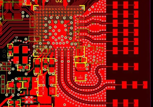
In RF circuits, the signal wavelength is typically much larger than the physical dimensions of circuit components and interconnections. For instance, at 100 MHz, the free-space wavelength is approximately 3 meters, making most circuit elements electrically small. This allows engineers to employ lumped parameter models, where passive components such as resistors (R), capacitors (C), and inductors (L) are treated as ideal, concentrated elements with well-defined values.
Under the lumped parameter assumption, circuit analysis relies heavily on traditional network theory, Kirchhoff’s laws, and conventional AC circuit analysis techniques. The primary design concerns in RF circuits include signal modulation and demodulation, noise figure optimization, power amplification efficiency, and bandwidth considerations. Engineers focus on component selection, biasing schemes, and impedance matching using discrete components or simple transmission line segments.
RF circuit design emphasizes the careful management of parasitic effects that become more pronounced at higher frequencies within the RF range. Parasitic capacitances between traces, lead inductances, and skin effect losses all require attention, but they can generally be modeled using equivalent circuit approaches with additional lumped elements.
Microwave Circuit Design Approach
Microwave circuits operate in a fundamentally different regime where signal wavelengths approach or become smaller than circuit dimensions. At 1 GHz, the free-space wavelength is 30 cm, while at 10 GHz, it reduces to 3 cm. When dealing with printed circuit board (PCB) traces, component packages, or waveguide structures of comparable dimensions, the lumped parameter approximation breaks down completely.
Instead, microwave circuit design relies on distributed parameter models that account for the wave nature of electromagnetic propagation. Every transmission line segment, interconnection, and even component mounting becomes a distributed element characterized by its electromagnetic field patterns, characteristic impedance, and propagation characteristics.
The design process shifts from component-centric thinking to field-theory-based analysis. Engineers must consider transmission line theory, S-parameters, Smith chart analysis, and electromagnetic field distributions. The concept of electrical length becomes crucial, as a physically short connection might represent multiple wavelengths at microwave frequencies, creating complex resonant behaviors and phase relationships.
Impedance Matching: From Simple to Sophisticated

Impedance matching represents one of the most critical aspects where RF and microwave circuits diverge significantly in complexity and approach. While both domains require careful impedance considerations, the methods and criticality levels differ substantially.
RF Impedance Matching
In RF circuits, impedance matching primarily focuses on maximizing power transfer and minimizing signal reflections using relatively straightforward techniques. Engineers typically employ L-section, π-section, or T-section matching networks composed of lumped capacitors and inductors. The Smith chart may be used, but often simplified impedance calculations suffice for many applications.
The consequences of imperfect matching in RF circuits, while undesirable, are often manageable through design margins and can sometimes be compensated by increased amplifier gain or improved filtering. Return loss requirements are typically less stringent, with values of -10 dB to -15 dB often considered acceptable for many applications.
Microwave Impedance Matching
Microwave circuits demand far more sophisticated impedance matching approaches due to the distributed nature of the system and the higher frequencies involved. The reflection coefficient (Γ) becomes a critical design parameter, defined by:
Γ = (Z_L – Z_0) / (Z_L + Z_0)
Where Z_L represents the load impedance and Z_0 represents the characteristic impedance of the transmission line system. Even small impedance mismatches can create significant signal reflections, leading to standing wave patterns that cause power loss, signal distortion, and potentially damaging voltage and current peaks.
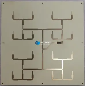
Microwave matching networks often employ distributed elements such as quarter-wave transformers, stub tuners, and complex multi-section matching structures. Advanced techniques include the use of microstrip lines, striplines, coaxial structures, and waveguide components. The Smith chart becomes an indispensable tool for visualizing complex impedance transformations and designing matching networks.
The precision required in microwave impedance matching is significantly higher, with return loss requirements often exceeding -20 dB or -30 dB. This level of precision demands careful consideration of manufacturing tolerances, temperature stability, and frequency variations across the operating band.
Component Technologies and Material Considerations
The choice of components and materials represents another major distinction between RF and microwave circuit design, driven by the different physical phenomena dominant at each frequency range.
RF Circuit Components
RF circuits commonly utilize conventional semiconductor devices such as bipolar junction transistors (BJTs), metal-oxide-semiconductor field-effect transistors (MOSFETs), and junction field-effect transistors (JFETs). These devices can provide adequate performance at RF frequencies, with careful attention to parasitic effects and package considerations.
Passive components in RF circuits include wire-wound inductors, ceramic or film capacitors, and carbon or metal film resistors. While parasitic effects must be considered, these components can often provide satisfactory performance when properly selected and applied.
LC filter networks remain viable options for many RF applications, although engineers must account for the Q-factor limitations and parasitic resonances that become more prominent at higher RF frequencies.
Microwave Circuit Components
Microwave circuits require specialized semiconductor technologies optimized for high-frequency operation. High-electron-mobility transistors (HEMTs), particularly those fabricated using gallium arsenide (GaAs) or gallium nitride (GaN) technologies, offer superior performance at microwave frequencies. These devices provide higher gain, better noise figures, and improved linearity compared to conventional silicon-based transistors.
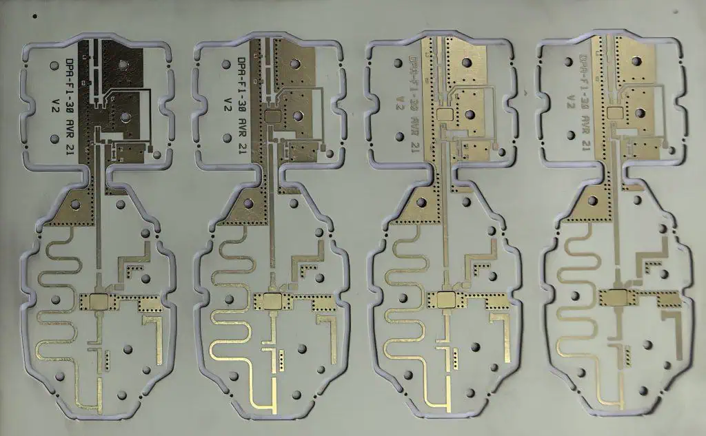
The transition to microwave frequencies often necessitates the abandonment of conventional lumped components in favor of distributed structures. Microstrip lines, striplines, and coplanar waveguides replace discrete inductors and capacitors. Resonant cavities, dielectric resonators, and surface acoustic wave (SAW) devices provide filtering functions with higher Q-factors and better temperature stability than possible with conventional LC networks.
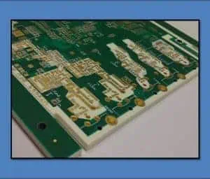
Material selection becomes critically important in microwave circuits, with low-loss dielectric materials such as polytetrafluoroethylene (PTFE), Rogers RO4000 series laminates, or specialized ceramics preferred for substrates. Conductor materials must exhibit low surface roughness and high conductivity to minimize losses due to skin effect and surface current distribution.
Loss Mechanisms and Performance Limitations
The dominant loss mechanisms in RF and microwave circuits reflect the different physical phenomena at work in each frequency regime, requiring distinct approaches to loss minimization and performance optimization.
RF Circuit Losses
RF circuits primarily contend with conductor losses due to the finite resistance of metallic conductors and the skin effect that concentrates current flow near conductor surfaces. As frequency increases within the RF range, skin depth decreases, effectively reducing the cross-sectional area available for current flow and increasing resistance.
Device noise represents another significant concern in RF circuits, particularly in receiver front-end applications where low noise figures are essential for maintaining system sensitivity. Thermal noise, shot noise, and flicker noise all contribute to the overall noise performance, with careful device selection and circuit topology optimization required to achieve optimal performance.
Dielectric losses in RF circuits, while present, are typically less critical than at microwave frequencies due to the lower operating frequencies and the use of materials with adequate loss tangent characteristics for RF applications.
Microwave Circuit Losses
Microwave circuits must address a more complex set of loss mechanisms that become increasingly significant at higher frequencies. In addition to enhanced conductor losses due to increased current crowding and skin effect, dielectric losses become a major concern.
Dielectric loss occurs when electromagnetic energy is absorbed by insulating materials, converting it to heat. The loss tangent (tan δ) of substrate materials becomes a critical parameter, as even small values can result in significant signal attenuation over the distributed structures common in microwave circuits. This necessitates the use of specialized low-loss materials and careful attention to substrate thickness and uniformity.
Radiation losses represent another unique challenge in microwave circuits, occurring when electromagnetic energy escapes from transmission lines or circuit structures and propagates into free space. This is particularly problematic in open structures such as microstrip lines, where fringing fields can couple to nearby conductors or radiate energy away from the intended signal path.
To combat radiation losses, microwave circuits often incorporate shielding structures, ground plane designs, and via fencing to contain electromagnetic fields within the intended circuit boundaries. The design of these structures requires careful electromagnetic simulation and optimization to achieve the desired performance while maintaining manufacturing feasibility.
Application Domains and System Requirements
The distinct characteristics of RF and microwave circuits make them suitable for different classes of applications, each with unique performance requirements and system constraints.
RF Applications
RF circuits dominate applications requiring moderate bandwidth, reasonable power efficiency, and cost-effective implementation. Short-range wireless communication systems such as Bluetooth, Zigbee, and WiFi (at 2.4 GHz) utilize RF circuit techniques. Radio broadcasting, amateur radio communications, and RFID systems all rely heavily on RF circuit design principles.
In these applications, the emphasis often lies on achieving adequate performance at minimum cost, with considerations for power consumption, battery life, and integration with digital signal processing systems. The relatively relaxed precision requirements compared to microwave systems allow for more straightforward design approaches and broader manufacturing tolerances.
Microwave Applications
Microwave circuits enable applications requiring high bandwidth, precise control of electromagnetic properties, and often operation at significant power levels. Radar systems represent a major application domain, where the ability to generate, amplify, and process high-frequency signals with precise timing and phase relationships is essential for accurate target detection and ranging.
Satellite communication systems rely extensively on microwave circuits for both ground-based and space-based equipment. The high frequencies enable practical antenna sizes while providing the bandwidth necessary for modern communication requirements. Microwave ovens represent a familiar consumer application where precise frequency control and high power generation are essential for effective operation.
Point-to-point communication links, particularly in telecommunications infrastructure, utilize microwave frequencies to achieve high data rates over long distances. These applications demand exceptional stability, low phase noise, and high spectral efficiency to maximize channel capacity within allocated frequency bands.
Future Trends and Convergence
As electronic systems continue to push toward higher frequencies and broader bandwidths, the distinction between RF and microwave circuits continues to evolve. Software-defined radio systems increasingly operate across both RF and microwave frequency ranges, requiring design approaches that can accommodate the transition between lumped and distributed parameter regimes.
The emergence of millimeter-wave applications, particularly in 5G cellular systems and automotive radar, is pushing microwave design techniques into even higher frequency ranges where new challenges in materials, packaging, and system integration arise. These trends suggest that understanding both RF and microwave design principles will become increasingly important for engineers working in modern high-frequency systems.
Conclusion
The fundamental differences between RF and microwave circuits stem from the frequency-dependent physical phenomena that govern electromagnetic wave behavior. The transition from lumped parameter models suitable for RF design to the distributed parameter approaches essential for microwave circuits represents more than just a change in analysis techniques—it reflects a fundamental shift in the physical behavior of electromagnetic energy.
Understanding these distinctions provides the foundation for successful high-frequency circuit design, enabling engineers to select appropriate design methodologies, components, and materials for their specific applications. As the boundaries between RF and microwave continue to blur in modern systems, mastery of both domains becomes essential for addressing the challenges of next-generation electronic systems.

