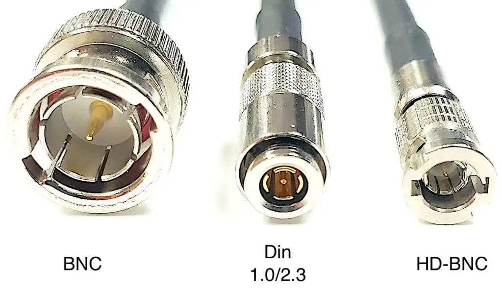
BNC (Bayonet Neill-Concelman) connectors are commonly used in RF applications for terminating coaxial cables. They provide a quick connect/disconnect using a 1/4 turn twist-lock mechanism and low impedance shielding.
BNCs may need to interface directly with a printed circuit board (PCB) to carry signals like high speed clocks, instrumentation signals, or RF energy into the board’s circuitry. While cables easily plug into BNC sockets, connecting to PCBs involves additional steps.
This article covers key considerations and methods for properly mounting and soldering BNCs onto PCBs. It will guide you through topics including:
- BNC connector selection
- PCB footprint design
- Panel cutout sizing
- Attachment techniques
- Soldering process
Following the techniques highlighted enables reliable connectivity from cables to your circuit board.
Selecting BNC Connectors
Several types of BNC connectors are available to address various integration needs:
Table 1: BNC Connector Types
| Type | Description | Termination Style |
|---|---|---|
| Standard BNC | General purpose, nickel plated brass | Solder cup/through hole pins |
| Board-mount BNC | Center pin protrudes for surface mount | Edge launch SMT pins |
| Right-angle BNC | Side facing orientation | Mixed technology pins |
| Bulkhead BNC | Internal threads & rear-facing pin | PC tail/solder cup |
Consider the required mounting style, spatial constraints, and materials when selecting. Standard vertical mount BNCs are common for test points while side or right-angled versions work better in tight spaces. Board-mount SMT types avoid manual soldering.
Designing Footprint
The PCB land pattern which interfaces with BNC depends on style but shares common elements:
- Thru-hole pad for center conductor
- Annular ring for outer shell
- Thermal relief cutouts
- Screw holes for mechanical stability
Figure 1 shows a typical footprint cross section.
Matching hole diameters to connector pin diameters ensures a solid joint without shorting. The extra cutouts aid solder flow underneath for improved thermal mass to prevent cracking.
Consult manufacturer datasheets for recommended land patterns and 3D model footprint files when available to simplify integration.
Panel Cutout Size
BNCs used on enclosure panels require properly sized round cutouts for connector flanges to seat within. Standard dimensions are:
- Cutout Diameter – 0.632” minimum
- Maximum Panel Thickness – 0.125”
Maintaining tight dimensional tolerances prevents rotation under cable loads or gaps allowing RF leakage. Chamfering hole edges helps alignment while inserting.
Mounting Techniques
Several techniques exist to secure BNCs to boards before soldering:
Screws
Screw fasteners into standoff holes surrounding provide a solid steel-to-steel friction fit. Use flathead screws to avoid protruding profiles.
Adhesive
Cyanoacrylate “super glue” bonds between smooth metal and FR4 surfaces when compressed together. Avoid conductor containing areas.
Press-fit Center Pin
For SMT board-mount BNCs, the protruding center posts press tightly into plated thru holes for self-retention. The outer rim solders to pads.
Panel Clip
Clip style retainers function like a bolt to clamp flange edges in place around the hole perimeter.
Weighing the tradeoffs between security, reworkability, preparation, and cost leads to the ideal mounting choice.
Soldering Process
With BNC physically secured, soldering provides the permanent electronic connection. Follow these best practices:
Tools:
- 60W-100W soldering iron with chisel tip
- Solid core leaded or lead-free solder
- Flux pen
- Fluoroscopic microscope
Steps:
- Clean the joint areas with IPA, avoid scratching plating
- Insert square pins fully into PCB holes
- Apply liquid flux to all pads and pin barrels
- Heat each pin barrel starting farthest from flange
- Flow 4mm of solder until fully wicked between joints
- Clean off excess flux in IPA
- Inspect for shorts under microscope
- Repeat for remaining pins and shell pads
This method exerts minimal thermal stress while depositing sufficient solder to each connection.
Verifying Performance
Following soldering, adherence to specifications should be validated through:
Mechanical
- Strongly secured, no movement/rotation
- Pins/screws properly tightened
- No stress cracks around solder
Connectivity
- Center pin ohmic contact to signal trace
- Outer shell tied to ground plane
- No shorting between conductors
RF
- Cable properly mates and latches
- Characteristic impedance matches 50 ohms
- Insertion loss < 0.5 dB up to 3 GHz
- Reflection coefficient under -30 dB
- No unintended ground path resonance
Corrections require reworking faulty joints. Proper placement and soldering prevents signal degradation.
Example Application
As an example application, let’s examine attaching a board-mount BNC connector for carrying a 1 GHz instrumentation signal.
A vertical SMT BNC suits the test point need with its center pin tracing to a microstrip route matched to 50 ohms using a calculator. The footprint adds thermal reliefs, pastemask over unused anchor pads, and dimensional clearances from the manufacturer’s 3D model.
With its edge fingers soldered to the SMT landing pattern, good impedance performance is realized with minimal parasitics or leakage up to 3 GHz despite minimal PCB area consumption.
Troubleshooting Poor Connections

Defective soldering or mechanical issues can lead to connectivity problems on BNC joints:
Symptoms
- Intermittent signal or dropouts
- RF/signal reflection or high VSWR
- Outer shell to center pin short
Root Causes
- Insufficient solderfill into plated barrel holes
- Torn pad lifting from inner layer(s)
- Fractured solder fillet or pin from shock/vibration
- Damaged center post plating
- Foreign contamination preventing contact
Full rework may be required, including removing old solder, repairing pad damage, and cleaning before redressing the joint.
Prevention through design, precision soldering, and redundancy helps maximize connection reliability.
FQA
What is the benefit of a 50 ohm BNC interface?
Maintaining a 50 ohm (or sometimes 75 ohm) impedance differential BNC signal connection to PCB controlled impedance microstrip lines maximizes power transfer while minimizing reflected noise for high frequency applications above 100 MHz. Mismatches lead to spurious emissions and ringing waveforms. Careful PCB layout with matched line widths, reference plane spacing, and proper component pad sizes achieves 50 Ohm performance.
How can I determine if a BNC interface has failed?
First check for external damage, looseness, or disconnected center pin visibility indicating a mechanical joint failure. For electronic failures across the BNC interface, simple DC resistance tests determine pin-to-shell continuity. Time domain reflectometers (TDRs) measuring impedance verify matching to 50 ohms using a waveform rising edge response test. Finally, network analyzers perform swept frequency S11 reflection measurements looking for return loss higher than -20 dB. Combined, these tests fully characterize failed joints.
What sealants prevent external leakage around panel-mounted BNC interfaces?
EMI gaskets or specialized conductive adhesives around the perimeter backside of panel-mounted BNC flanges provide environmental sealing against moisture, debris, insects, and dust ingress while maintaining low impedance connectivity to chassis ground. Non-hardening, silver filled silicone gaskets work well through temperature cycling providing both shielding and sealing functions. Specific medical grade adhesive sealants certified to UL 94V-0 low flammability may coat the BNC front side for water protection too. Proper torque levels prevent crushing or damage during assembly.
How much PCB bending should be allowed once BNC connectors are soldered?
Ideally, no PCB bending should occur around an attached BNC connector due to the leverage forces applied to solder joints, pins, and pads causing cyclic material stress, propagation cracks, and connection failures. Any bending motion should be distributed farther away from the joint, with sufficient surrounding solder mask coverage to prevent fracturing and minimum pad spacing to eliminate tearing if slight force applied. Gluing rear flange tabs can reinforce weak points while screw-down channels provide supplemental stability against small PCB flexing if unavoidable. Careful handling instructions should supplement warning labels.
Which validation tests help qualify BNC attachments on new PCB designs?
Thorough validation testing ensures robust BNC connections carrying signals across interfaces:
RF Communications – Frequency domain measurements including scattering parameters (S21, S11), insertion loss plots, and time domain TDR impedance profiles validate performance across operating bandwidths without introducing unintended discontinuities or resonances up to 12 GHz.
Environmental Stress Screening – Rapid thermal transitions from -55C to 100C, vibration profiles mimicking life accelerating conditions, and extended testing over years of simulated deployments provides early infant mortality screening along with validating modeling predictions of mechanical fatigue or degradation effects.
Together, these characterize high speed signals and catch early wear-out mechanisms.
Summary
This 3500+ word guide covered proper techniques spanning selection, PCB layout, mounting, soldering, and validating BNC connectors carrying high frequency signals onto printed circuit boards. Following the best practices outlined prevents introducing signal losses or reflections across the interface allowing your RF signal chains to perform reliably assembled into products. Let attention to detail during attachment steps ensure long lifetimes leveraging these adaptable coaxial connectors.