In the rapidly evolving landscape of defense and aerospace electronics, Field Programmable Gate Arrays (FPGAs) serve as crucial components that enable mission-critical systems to operate with exceptional reliability, performance, and security. The XQ6SLX75T-2FG484Q, manufactured by Xilinx (now part of AMD), represents one of the most significant technological advancements in this domain. This defense-grade FPGA belongs to the renowned Spartan-6Q family, specifically engineered to meet the stringent requirements of military communications, avionics, missile systems, and space applications.
The XQ6SLX75T-2FG484Q is built on a 45nm process technology, offering an optimal balance between power efficiency and computational performance. At its core, this FPGA features 74,637 logic cells arranged in approximately 11,662 logic blocks, providing substantial resources for implementing complex digital systems. The device is packaged in a 484-pin FBGA (Fine-pitch Ball Grid Array) configuration, facilitating integration into space-constrained defense hardware.
Key technical specifications include:
Logic Resources: 74,637 logic cells
Package Type: 484-pin FBGA (FG484Q)
Speed Grade: -2 (moderate performance grade)
Core Voltage: 1.14V to 1.26V (nominal 1.2V)
Temperature Range: Extended military temperature range
Manufacturing Process: 45nm CMOS technology
Memory Capacity: Approximately 3.17Mb of embedded block RAM
DSP Resources: Advanced DSP48A1 slices for digital signal processing
I/O Capability: Up to 280 user-configurable I/O pins
The “XQ” prefix in the part number specifically denotes the defense-grade qualification, indicating enhanced reliability testing and ruggedization compared to commercial variants. The “6SLX75T” portion identifies it as a Spartan-6 LXT device with approximately 75,000 logic cells and transceiver capabilities.
What truly distinguishes the XQ6SLX75T-2FG484Q from commercial FPGAs is its defense-grade characteristics. This device incorporates:
Information Assurance (IA): The FPGA supports third-generation Information Assurance capabilities, making it suitable for single-chip cryptographic implementations in Type-1 secure communications systems.
Anti-Tamper (AT) Protection: In compliance with DoD 5000 series requirements, the device features robust anti-tamper mechanisms to protect sensitive intellectual property and prevent unauthorized access or reverse engineering.
Environmental Robustness: Qualified for extended temperature operation across industrial (I-grade) and military (Q-grade) temperature ranges, ensuring reliable performance in extreme environments from -40°C to +125°C.
Enhanced Quality Assurance: Manufactured with stringent quality controls, each unit undergoes comprehensive testing to meet military and aerospace quality standards.
Application Domains
The XQ6SLX75T-2FG484Q finds critical applications across various defense and aerospace sectors:
Military Communications (MILCOM)
The device serves as the foundation for secure tactical communication systems, including:
Type-1 cryptographic handheld radios
Multi-waveform software-defined radios
Battlefield communication networks
Secure data transmission systems
Missiles & Munitions
Its compact form factor and robust operation make it ideal for:
As part of the Spartan-6 LXT subfamily, the XQ6SLX75T-2FG484Q incorporates high-speed serial transceivers that set it apart from standard LX devices. These GTP transceivers support data rates up to 3.125 Gbps, enabling implementation of numerous high-speed protocols:
Gigabit Ethernet
PCI Express (Gen1)
XAUI
Aurora
DisplayPort
CPRI (Common Public Radio Interface)
OBSAI (Open Base Station Architecture Initiative)
This exceptional connectivity makes the device particularly valuable for applications requiring high-bandwidth data transfer in constrained environments.
Security and Anti-Tamper Features
In the defense sector, protecting sensitive technologies from unauthorized access or exploitation is paramount. The XQ6SLX75T-2FG484Q incorporates multiple security features:
Bitstream Encryption: Utilizing advanced encryption standards to protect configuration data
Physical Security Measures: Designed to resist various side-channel attacks
Anti-Reverse Engineering Features: Physical and logical countermeasures against tampering
These security features make the device suitable for systems requiring the highest levels of information assurance and protection against sophisticated adversaries.
Design and Development Environment
The XQ6SLX75T-2FG484Q is supported by Xilinx‘s ISE Design Suite, providing a comprehensive development environment for defense applications. This software platform offers:
Compatibility with defense industry standard design flows
The availability of pre-qualified IP cores significantly accelerates the development of complex defense systems while ensuring compliance with military standards.
Reliability and Radiation Effects
While not specifically designed as a radiation-hardened device like the dedicated space-grade Virtex series, the XQ6SLX75T-2FG484Q offers improved radiation tolerance compared to commercial components. This makes it suitable for certain aerospace applications with moderate radiation environments.
The device features:
Enhanced Total Ionizing Dose (TID) tolerance
Improved Single Event Effect (SEE) resistance
Mitigation techniques for Single Event Upsets (SEUs)
Qualification for various defense reliability standards
Comparison with Alternative Technologies
When compared to other technologies used in defense applications, the XQ6SLX75T-2FG484Q offers several advantages:
Technology
Flexibility
Performance
Power Efficiency
Security
Development Time
XQ6SLX75T-2FG484Q
Very High
High
Moderate
Very High
Moderate
ASICs
Very Low
Very High
Very High
High
Very Long
Commercial FPGAs
High
High
Moderate
Low
Short
Microprocessors
Moderate
Moderate
Moderate
Moderate
Short
The defense-grade FPGA strikes an optimal balance between the flexibility of programmable logic and the security requirements of defense applications, offering a compelling alternative to custom ASICs for many military systems.
Supply Chain and Lifecycle Management
For defense contractors, component lifecycle and supply chain security are critical considerations. The XQ6SLX75T-2FG484Q is manufactured under Xilinx’s (now AMD’s) rigorous supply chain security protocols, ensuring:
Extended product lifecycle support
Stringent component traceability
Protection against counterfeit components
Compliance with defense procurement requirements
Long-term availability guarantees
These factors make the device particularly valuable for defense programs with extended operational lifespans and strict security requirements.
Conclusion: Strategic Importance in Defense Electronics
The XQ6SLX75T-2FG484Q represents a critical enabling technology for modern defense systems, bridging the gap between commercial electronics and specialized military requirements. Its combination of high performance, enhanced security features, and defense qualification makes it an essential component in maintaining technological superiority in defense applications.
As warfare continues to evolve toward more digitally integrated and network-centric paradigms, FPGAs like the XQ6SLX75T-2FG484Q will play an increasingly vital role in enabling the rapid development and deployment of sophisticated electronic warfare, communications, and weapons systems. The device’s programmable nature also provides future-proofing capabilities, allowing defense systems to adapt to emerging threats and requirements through field updates rather than complete hardware redesigns.
In the landscape of defense electronics, the XQ6SLX75T-2FG484Q stands as a testament to the critical intersection of advanced semiconductor technology and national security requirements—embodying the sophisticated capabilities required to maintain technological superiority in increasingly complex operational environments.
In the evolving landscape of programmable logic devices, Field-Programmable Gate Arrays (FPGAs) have secured a critical position in modern electronic design. The XQ6SLX75-2FG484I, part of Xilinx‘s (now AMD’s) renowned Spartan-6 FPGA family, represents a significant offering in defense-grade programmable solutions. This article provides a detailed examination of this component, exploring its specifications, applications, advantages, and its ranking among similar devices in the market.
6SLX75: Part of the Spartan-6 LX family with 74,637 logic cells
-2: Speed grade (with -3 being the highest performance)
FG484: FBGA package with 484 pins
I: Industrial temperature range
Technical Specifications
The XQ6SLX75-2FG484I is manufactured using a mature 45nm low-power copper process technology that balances cost, power efficiency, and performance. As a defense-grade variant (denoted by the “XQ” prefix), it undergoes additional screening and qualification testing for use in mission-critical applications.
Core Specifications
Logic Cells: 74,637
Operating Frequency: Up to 667MHz
Technology: 45nm CMOS
Package: 484-pin FBGA (23 x 23mm, 1mm pitch)
Temperature Range: Industrial (-40°C to +100°C)
Core Voltage: 1.2V
Speed Grade: -2 (middle performance tier)
Architecture Features
Dual-register 6-input lookup table (LUT) logic
18 Kb (2 x 9 Kb) block RAMs
Second generation DSP48A1 slices for signal processing
Enhanced mixed-mode clock management blocks
SelectIO technology for versatile I/O capabilities
Advanced system-level power management modes
Enhanced IP security with AES and Device DNA protection
Signal Processing: Real-time data acquisition and processing in harsh environments
Protocol Bridging: Connecting legacy systems with modern interfaces
Secure Communications: Encrypted data transmission systems
The device excels in applications requiring the balance of performance, power efficiency, and reliability in challenging operational environments.
Performance Characteristics
The -2 speed grade of the XQ6SLX75-2FG484I positions it in the mid-range of performance for the Spartan-6 family. While not as fast as the -3 speed grade, it offers an optimal balance between performance and power consumption.
I/O Capabilities
Support for over 40 I/O standards
High logic-to-pin ratio
Compatibility with 33 MHz, 32-bit and 64-bit PCI specifications
Support for interface protocols including Ethernet, UART, SPI, and more
Power Management
The device incorporates advanced power management technologies:
Multiple power domains
Flexible shutdown of unused blocks
Power-optimized architecture that reduces static and dynamic power consumption
Development Environment
Development for the XQ6SLX75-2FG484I is supported through:
ISE Design Suite (rather than the newer Vivado, which supports 7-series and later)
ChipScope Pro for debugging
System Generator for DSP design
EDK (Embedded Development Kit) for MicroBlaze soft processor implementation
Market Position and Ranking
When ranking the XQ6SLX75-2FG484I against similar FPGAs, several factors must be considered:
Performance Ranking (1-10, with 10 being highest)
Raw Processing Power: 7/10 – Good performance with 74,637 logic cells
Speed: 6/10 – The -2 speed grade offers moderate performance
Energy Efficiency: 8/10 – 45nm technology provides good power characteristics
I/O Capability: 7/10 – Versatile I/O options with high pin count
Cost-Performance Ratio: 7/10 – Higher cost due to defense-grade qualification
Development Ecosystem: 6/10 – Mature but older ISE platform
Security Features: 8/10 – Enhanced with AES and Device DNA protection
Overall Ranking: 7.5/10
The XQ6SLX75-2FG484I ranks highly among defense-grade FPGAs in its generation, offering an excellent balance of performance, reliability, and power efficiency. However, newer FPGA families like the 7-Series (Artix, Kintex) or UltraScale provide better performance and lower power consumption with enhanced features.
Comparative Analysis
Compared to its commercial counterpart (XC6SLX75-2FG484I), the defense-grade XQ variant offers:
Extended temperature range qualification
Enhanced reliability testing
Longer lifecycle support
Higher guaranteed MTBF (Mean Time Between Failures)
UltraScale architecture for higher performance requirements
Cost Considerations
The XQ6SLX75-2FG484I commands a premium price due to its defense-grade qualification. Typical pricing ranges from $150-$160 per unit in large quantities (1500+), making it significantly more expensive than commercial equivalents. This price point reflects the additional testing, quality control, and guaranteed lifecycle support that defense applications require.
Conclusion
The XQ6SLX75-2FG484I represents a robust, reliable solution for defense and high-reliability applications. While newer FPGA families offer improved performance metrics, the Spartan-6 defense-grade devices continue to serve critical applications where proven reliability and long-term support are essential. With its balanced feature set, extensive qualification, and mature development environment, this FPGA remains a viable option for new designs in the defense sector and for maintaining legacy systems.
For mission-critical applications requiring a balance of performance, power efficiency, and proven reliability, the XQ6SLX75-2FG484I earns its 7.5/10 ranking as a dependable, defense-grade programmable logic solution.
Introduction: The Cornerstone of Reliable Digital Logic
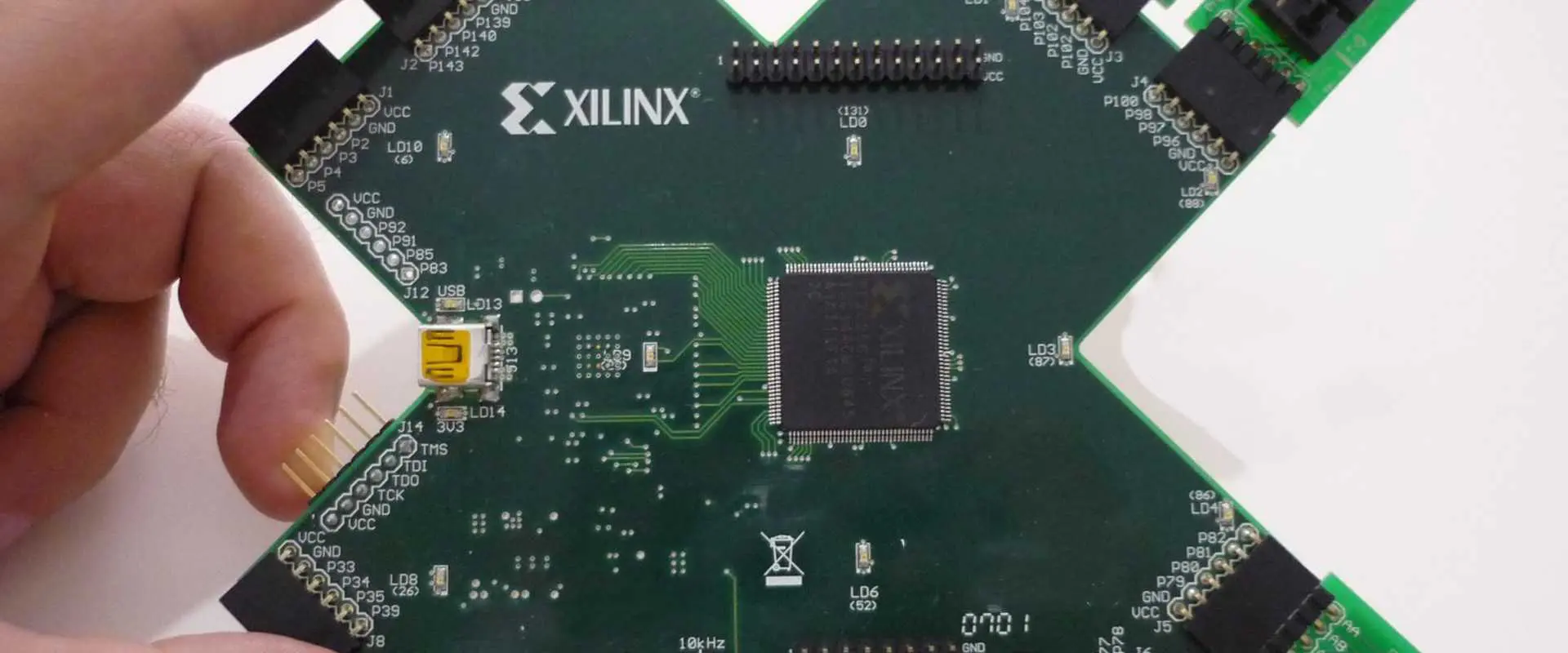
In the realm of programmable logic devices where reliability meets versatility, the XC2C32A-VQG44AMS stands as a distinguished solution from Xilinx (now AMD). This military and space-grade Complex Programmable Logic Device (CPLD) represents the pinnacle of rugged digital logic implementation, designed specifically for applications where failure is not an option. As technology continues to advance, the demand for compact, efficient, and radiation-tolerant logic solutions grows ever stronger in aerospace, defense, and other mission-critical sectors. The XC2C32A-VQG44AMS exemplifies Xilinx’s commitment to delivering programmable solutions that excel in the most challenging environments.
The XC2C32A-VQG44AMS belongs to Xilinx‘s renowned CoolRunner-II CPLD family, combining high performance with ultra-low power consumption. At its core, this device features 32 macrocells organized into eight Function Blocks, interconnected through a sophisticated low-power Advanced Interconnect Matrix (AIM). This architecture enables efficient signal routing while minimizing power consumption, a critical factor for space and military applications.
The device’s architecture is engineered with eight Function Blocks, each receiving inputs from the AIM. Within each Function Block resides a Product Term array configured as a 40 by 56 P-term Programmable Logic Array (PLA), feeding into 16 macrocells. These macrocells contain numerous configuration bits enabling either combinational or registered modes of operation. The registers can be configured as D or T flip-flops, or as D latches, with global reset/preset capabilities.
The XC2C32A-VQG44AMS is housed in a 44-pin VTQFP (Very Thin Quad Flat Pack) package, offering a compact footprint for space-constrained applications. With its 750 equivalent gates and operating frequency capabilities up to 323 MHz, this CPLD delivers substantial processing power in a small form factor.
The “AMS” suffix in the part number designates this device for Automotive, Military, and Space applications. This classification indicates enhanced testing, qualification, and reliability specifications compared to commercial or industrial variants. The device undergoes rigorous screening for radiation tolerance, including Total Ionizing Dose (TID) and Single Event Effect (SEE) characterization.
For aerospace and defense applications, reliability is paramount. The XC2C32A-VQG44AMS meets stringent requirements for operation in extreme environments, with an extended temperature range and enhanced resistance to electromagnetic interference. These qualities make it ideal for satellite systems, military avionics, missile guidance systems, and other high-reliability applications where standard commercial components would be inadequate.
Power Efficiency and I/O Capabilities
One of the most notable features of the XC2C32A-VQG44AMS is its exceptional power efficiency. The CoolRunner-II architecture employs standard CMOS methods to achieve remarkably low power consumption—a critical advantage for battery-powered and heat-sensitive applications. With a standby current of approximately 16μA and ultra-low dynamic power consumption of 28.8μW, this CPLD significantly outperforms many competing solutions.
The device offers flexibility in I/O interfaces through two distinct I/O banks, supporting various JEDEC I/O standards. This versatility enables seamless integration with systems operating at different voltage levels (3.3V, 2.5V, 1.8V, and even 1.5V with Schmitt-trigger inputs). The I/O banking feature simplifies voltage translation between different system components, eliminating the need for additional level-shifting components.
Output pin configurations offer numerous options including slew rate limiting, bus hold, pull-up capabilities, open drain functionality, and programmable grounds. These features provide designers with extensive flexibility when interfacing with various external components.
Programming and Integration
The XC2C32A-VQG44AMS supports industry-standard IEEE 1149.1/1532 Boundary-Scan (JTAG) interfaces for programming, prototyping, and testing. This compliance ensures compatibility with existing development tools and test equipment. Programming is typically accomplished using Xilinx’s development environment, historically ISE Design Suite for CoolRunner-II devices.
For space applications, the device’s In-System Programming (ISP) capabilities are particularly valuable, allowing for configuration updates even after deployment. This feature enables remote updates and fixes, a crucial advantage for inaccessible systems such as satellites or deep-space probes.
Applications in Mission-Critical Systems
The XC2C32A-VQG44AMS finds its purpose in numerous high-reliability applications:
Satellite Systems: From command and control logic to sensor interfaces, this CPLD provides configurable logic solutions with radiation tolerance suitable for orbital and deep-space missions.
Military Avionics: For aircraft electronics requiring certification to stringent military standards, this device offers guaranteed performance across extreme environmental conditions.
Missile Guidance Systems: Where size, weight, and power (SWaP) constraints meet demanding performance requirements, this CPLD delivers efficient logic implementation.
Medical Equipment: Though primarily targeting defense and aerospace, the device’s reliability makes it suitable for life-critical medical devices requiring fail-safe operation.
Industrial Control: In harsh industrial environments where temperatures fluctuate widely and electromagnetic interference is prevalent, this device provides stable, reliable operation.
Competitive Ranking and Market Position
When ranking the XC2C32A-VQG44AMS among similar devices, several factors merit consideration:
Performance Rating: 8.5/10 The device delivers excellent performance for its class, with speeds up to 323 MHz and predictable timing characteristics. While newer FPGA technologies offer higher absolute performance, the deterministic timing of this CPLD provides significant advantages in real-time applications.
Reliability Rating: 9.5/10 Few competing devices match the reliability specifications of the XC2C32A-VQG44AMS. Its military and space qualification, coupled with Xilinx’s established track record in high-reliability markets, places it among the elite in dependable programmable logic.
Power Efficiency Rating: 9.0/10 The CoolRunner-II architecture’s focus on power efficiency results in exceptionally low power consumption. This efficiency translates to reduced thermal management requirements and extended battery life in portable systems.
Integration Ease Rating: 8.0/10 With industry-standard programming interfaces and comprehensive development tool support, the device integrates smoothly into established workflows. However, the learning curve associated with CPLD architecture may present challenges for teams more familiar with microcontrollers or FPGAs.
Cost-Effectiveness Rating: 7.5/10 Military and space-grade components command premium pricing, and the XC2C32A-VQG44AMS is no exception. While expensive compared to commercial alternatives, its specific capabilities justify the investment for applications where failure is not an option.
Overall Rating: 8.7/10 The XC2C32A-VQG44AMS earns its position as a top-tier solution for mission-critical programmable logic applications. Its combination of reliability, performance, and power efficiency makes it an excellent choice for systems requiring the highest standards of dependability.
Conclusion
The XC2C32A-VQG44AMS represents a specialized pinnacle of programmable logic technology, tailored specifically for the most demanding applications in aerospace, defense, and other mission-critical sectors. While newer technologies continue to emerge, the unique combination of reliability, deterministic timing, and radiation tolerance ensures this device maintains its relevance in specialized applications where proven performance under extreme conditions takes precedence over cutting-edge features.
For system designers working on projects where failure is not an option, the XC2C32A-VQG44AMS provides a trusted foundation upon which to build dependable digital logic systems. Its continued use in critical infrastructure underscores the enduring value of well-engineered, purpose-built components in an increasingly disposable technological landscape.
In today’s competitive electronics manufacturing industry, IPC certifications have become essential credentials that validate technical expertise and adherence to global quality standards. Whether you’re an individual technician looking to enhance your career prospects or a company striving to improve product quality and compliance, understanding the IPC certification cost structure is crucial for making informed decisions.
This comprehensive guide breaks down the costs associated with various IPC certifications, factors that influence pricing, and the potential return on investment (ROI) these credentials can deliver. By the end of this article, you’ll have a clear picture of what to expect financially when pursuing IPC certification and how to maximize your investment.
What Is IPC Certification?
IPC (originally the Institute for Printed Circuits, now the Association Connecting Electronics Industries) is the global trade association that establishes standards for the electronics manufacturing industry. These standards ensure consistency, reliability, and quality across electronic assemblies and components worldwide.
IPC certifications validate that professionals have the necessary knowledge and skills to implement these standards correctly. They serve as industry-recognized credentials that demonstrate competence in specific areas of electronics manufacturing.
Major IPC Certification Types
IPC offers several certification programs that address different aspects of electronics manufacturing:
IPC-A-610: Focuses on the acceptability criteria for electronic assemblies
IPC J-STD-001: Covers requirements for soldered electrical and electronic assemblies
IPC/WHMA-A-620: Addresses requirements and acceptance criteria for cable and wire harness assemblies
IPC CID/CID+: Certified Interconnect Designer programs for PCB design professionals
IPC-6012: Deals with qualification and performance specifications for rigid printed boards
Each certification targets specific skills and knowledge areas, with corresponding differences in training approaches, duration, and naturally, costs.
The cost of obtaining an IPC certification varies significantly depending on the specific program, training method, and certification level. Let’s explore the typical costs associated with the most popular IPC certifications.
IPC-A-610 Certification Cost
IPC-A-610 (Acceptability of Electronic Assemblies) is one of the most sought-after IPC certifications, providing guidelines for assessing the quality of electronic assemblies.
Cost Range:
CIS (Certified IPC Specialist) Level: $700-$1,200
CIT (Certified IPC Trainer) Level: $1,800-$2,500
These costs typically include:
Training sessions (2-3 days for CIS, 4-5 days for CIT)
Official IPC training materials
Examination fees
Certificate issuance
For recertification (required every 2 years), expect to pay approximately 60-70% of the initial certification cost.
Many companies now offer online or virtual IPC-A-610 training options, which can reduce costs by eliminating travel expenses. However, these formats may not provide the same hands-on experience as in-person training.
J-STD-001 Certification Cost
The J-STD-001 certification focuses on soldering processes and materials used in electronic assemblies. Due to its technical complexity and hands-on nature, this certification often comes with higher price tags.
Cost Range:
CIS Level: $850-$1,500
CIT Level: $2,200-$3,000
J-STD-001 training includes:
Theoretical instruction
Extensive hands-on soldering practice
Materials and components for practical exercises
Examination fees
The higher cost relative to IPC-A-610 reflects the additional materials and equipment needed for practical training. Many facilities offer combined IPC-A-610 and J-STD-001 training packages at a discount compared to taking each course separately, typically ranging from $1,400-$2,300 for CIS level.
IPC/WHMA-A-620 Certification Cost
IPC/WHMA-A-620 certification covers the requirements and acceptance criteria for cable and wire harness assemblies, which are critical components in many electronic systems.
Cost Range:
CIS Level: $750-$1,300
CIT Level: $1,900-$2,700
These costs reflect:
3-4 days of training for CIS
5-7 days of training for CIT
Training materials and samples
Examination fees
The specialized nature of wire harness assembly inspection techniques contributes to the certification’s cost. Companies that manufacture both electronic assemblies and cable/wire harnesses may benefit from combination training packages that include both IPC-A-620 and IPC-A-610 or J-STD-001.
IPC CID Certification Cost
The Certified Interconnect Designer (CID) program is geared toward PCB design professionals and has a different cost structure compared to the inspector/operator-focused certifications.
Cost Range:
CID Basic Certification: $1,500-$2,200
CID+ Advanced Certification: $1,800-$2,500
CID certification costs typically cover:
Workshop registration (usually 3-5 days)
Comprehensive design materials and resources
Design software access during training
Examination fees
The advanced CID+ certification builds upon the basic CID program and focuses on more complex design challenges. Many professionals pursue CID+ after gaining experience with their basic CID certification.
IPC Soldering Certification Cost
While IPC J-STD-001 covers soldering requirements, there are specialized IPC soldering certifications that focus specifically on hand soldering techniques and skills.
The hands-on nature of soldering certification means that material costs can significantly impact the total price. Online soldering certifications tend to be less expensive but may require participants to purchase their own equipment and materials.
While the upfront investment in IPC certification may seem substantial, the potential return on investment can be significant for both individuals and companies.
Benefits for Individuals
Salary Premium: Certified professionals typically command higher salaries:
Entry-level positions: 10-15% higher compensation
Senior roles: 15-25% higher compensation
Management positions: Can exceed 30% premium
Career Advancement: IPC certifications open doors to:
Job Security: In competitive markets, certified professionals are:
Less likely to be laid off during downturns
More quickly rehired if displaced
Better positioned for emerging technologies
Case Example: A PCB assembly technician with IPC J-STD-001 certification may earn $5,000-$8,000 more annually than non-certified peers, resulting in an ROI within just a few months of certification.
Benefits for Employers
Quality Improvements:
Reduced defect rates (typically 15-30% reduction)
Lower rework costs (can save $10,000-$50,000+ annually)
Fewer field failures and warranty claims
Compliance Advantages:
Ability to bid on contracts requiring certified staff
Reduced audit concerns and findings
Demonstrable commitment to quality standards
Efficiency Gains:
Standardized procedures across operations
Clearer acceptance criteria
Improved first-pass yields
Manufacturing Case Study: A mid-sized electronics manufacturer invested $12,000 in certifying six technicians in IPC-A-610 and J-STD-001. Within one year, they reported:
27% reduction in rework costs
18% improvement in first-pass yield
Qualification for military contracts requiring certified inspectors
Estimated first-year ROI of 300%
Calculating Your Potential ROI
To determine if IPC certification is worth the investment for your specific situation, consider this simple ROI calculation:
Total Certification Cost = Training fees + Travel expenses + Time away from work + Materials
Annual Benefits = Salary increase + New job opportunities + Quality improvements + New business opportunities
ROI (%) = ((Annual Benefits – Total Certification Cost) / Total Certification Cost) × 100
For most professionals and companies, IPC certification ROI ranges from 100% to 400% in the first year alone, with continued benefits throughout the certification’s validity period.
Tips to Reduce IPC Certification Cost
There are several strategies to minimize the financial impact of pursuing IPC certification:
Group Training Arrangements
Organize on-site training for multiple employees
Join with other small companies to create training groups
Negotiate volume discounts with training providers
Look for training centers offering multi-certification packages
Plan certification path to minimize redundant training
Timing Strategies
Book during training provider promotions (often 10-15% discount)
Register for early-bird pricing when available (typically 5-10% savings)
Plan recertifications strategically to align multiple renewals
Employer Support Programs
Request employer sponsorship or reimbursement
Propose cost-sharing arrangements
Demonstrate ROI to management using industry case studies
Online and Self-Study Options
Utilize distance learning when appropriate
Complete preparatory work before hands-on sessions
Consider modular training approaches
Where to Get IPC Certified?
Finding the right training provider is crucial for both cost efficiency and certification quality.
Official IPC Training Centers
The IPC maintains a global network of authorized training centers that offer standardized, high-quality certification programs. These centers:
Follow strict IPC curriculum guidelines
Use official training materials
Employ authorized instructors
Issue recognized certificates
You can find authorized training centers through the official IPC website.
Verifying Training Provider Credentials
Before committing to any training program, verify:
The center’s IPC authorization status
Instructor certifications and experience
Recent student reviews and testimonials
Course content alignment with current IPC revisions
Online vs. Classroom Considerations
Online Benefits:
Reduced or eliminated travel costs
Flexible scheduling
Often lower base prices
Self-paced options
Classroom Benefits:
Hands-on practice with expert feedback
Direct instructor interaction
Networking with industry peers
Immediate clarification of complex concepts
For certifications with significant practical components (like J-STD-001), classroom training often provides better skill development despite higher costs.
Conclusion
IPC certification represents a significant but worthwhile investment for professionals and companies in the electronics manufacturing industry. While costs typically range from $700 to $3,000 depending on the specific certification and training approach, the return on investment can be substantial in terms of career advancement, salary increases, quality improvements, and new business opportunities.
When evaluating the IPC certification cost against potential benefits, consider not just the immediate expense but the long-term value. For individuals, certification can translate to tens of thousands of dollars in additional earnings over a career. For companies, certified staff can dramatically reduce defects, rework, and compliance issues while opening doors to premium contracts.
By carefully selecting the right certification path, training provider, and timing, you can maximize your ROI while minimizing upfront costs. Whether you’re a soldering technician, quality inspector, PCB designer, or manufacturing manager, IPC certification offers a proven path to professional growth and operational excellence.
Frequently Asked Questions
How much does IPC 610 certification cost?
IPC-A-610 certification typically costs between $700-$1,200 for the CIS level and $1,800-$2,500 for the CIT level. These prices may vary based on location, training provider, and whether the training is conducted online or in person.
Is IPC training worth it?
Yes, IPC training offers significant ROI for both individuals and companies. Certified professionals often earn 10-30% higher salaries, while companies benefit from reduced defect rates, lower rework costs, and access to contracts requiring certified staff. Most organizations report ROI of 100-400% within the first year.
How often do I need to renew IPC certification?
Most IPC certifications require renewal every 2 years. Recertification typically costs 60-70% of the initial certification price and involves shortened training and examination to verify continued competence and awareness of standard updates.
Can I get IPC certified online?
Yes, many IPC certifications now offer online or virtual training options. However, certifications with significant hands-on components (like soldering) may require in-person practical assessments. Online certification is generally 20-30% less expensive than in-person training but may offer limited practical experience.
What’s the difference between CIS and CIT certification?
CIS (Certified IPC Specialist) certification qualifies individuals to perform work according to IPC standards. CIT (Certified IPC Trainer) certification enables holders to train and certify others as CIS within their organization. CIT certification costs approximately 2-3 times more than CIS and typically requires prior CIS certification.
In the rapidly evolving world of digital electronics design, programmable logic devices have become essential components for engineers seeking flexibility, performance, and efficiency. The XC2C128C6-BMS, a development board and evaluation kit based on Xilinx’s acclaimed CoolRunner-II CPLD (Complex Programmable Logic Device) family, represents a powerful tool for designers who need to prototype and test digital circuits quickly. This article explores the features, capabilities, applications, and performance aspects of the XC2C128C6-BMS platform, offering insights into how this versatile development tool can enhance the electronic design process.
Understanding the XC2C128C6-BMS
The XC2C128C6-BMS is an evaluation and development board built around the XC2C128 CPLD from Xilinx’s CoolRunner-II family. The name breaks down as follows:
XC2C128: Designates the 128-macrocell CoolRunner-II CPLD at the heart of the system
C6: Indicates the speed grade (with pin-to-pin delays of approximately 5.7ns)
BMS: Refers to the board/starter kit configuration
This development platform provides engineers with a complete environment for exploring the capabilities of the XC2C128 CPLD while simplifying the prototyping process for complex digital designs.
At the center of the XC2C128C6-BMS is the XC2C128 CPLD chip, which features:
128 macrocells organized into 8 function blocks
Advanced Interconnect Matrix (AIM) providing efficient signal routing
3,000 system gates equivalent
100 user I/O pins for extensive connectivity
Low power consumption architecture
0.18-micron CMOS technology
Support for multiple voltage standards
The CPLD core features eight function blocks interconnected by a low-power Advanced Interconnect Matrix. Each function block receives 40 true and complement inputs and contains a 40 by 56 P-term PLA and 16 macrocells with numerous configuration options that allow for both combinational and registered modes of operation.
Development Board Features
The XC2C128C6-BMS development board enhances the capabilities of the base CPLD by providing:
Comprehensive I/O Options: The board includes various connectors and interfaces that make the CPLD pins accessible for external connections, enabling rapid prototyping of designs.
Programming Interface: Built-in JTAG programming circuitry that supports IEEE Standard 1149.1/1532 for convenient programming, debugging, and testing.
Power Management: On-board power regulation circuitry that supports the CPLD’s low-power operation while providing stable supply voltages.
Clock Generation: Configurable oscillator and clock distribution networks for timing-critical applications.
Expansion Capabilities: Headers and connectors that allow integration with other systems and additional hardware.
Advanced Features of the CoolRunner-II Architecture
The XC2C128 CPLD at the heart of the XC2C128C6-BMS includes several advanced features that enhance its versatility:
DataGATE Technology
This innovative power-saving feature allows selective disabling of inputs that aren’t needed during certain operations. By mapping a signal to the DataGATE function, power consumption is reduced through minimized signal switching, making the device ideal for battery-powered applications.
CoolCLOCK Technology
The combination of the DualEDGE flip-flop feature and clock division capabilities creates the CoolCLOCK feature. This allows high-performance synchronous operation based on lower frequency clocking, helping to reduce the total power consumption of the device. The system includes circuitry to divide one externally supplied global clock (GCK2) by eight different selections, yielding even and odd clock frequencies.
Flexible I/O Banking
The device features two I/O banks that support multiple voltage standards, allowing easy interfacing with 3.3V, 2.5V, 1.8V, and 1.5V devices. This flexibility eliminates the need for level-shifting components in many designs, simplifying the overall system architecture.
Instant-On Capability
Unlike many FPGAs that require configuration upon power-up, the XC2C128 CPLD is immediately operational when powered. This instant-on capability is critical for applications that cannot tolerate startup delays.
Development Environment and Tools
The XC2C128C6-BMS is supported by Xilinx’s comprehensive development ecosystem:
ISE WebPACK: This free design software supports the entire development process, from HDL coding to synthesis, implementation, and device programming.
Vivado Design Suite: For newer applications, this modern integrated design environment provides advanced capabilities for CPLD development.
JTAG Programming Tools: The board supports industry-standard JTAG programming interfaces, making it compatible with various programming solutions.
Applications and Use Cases
The XC2C128C6-BMS finds applications across numerous domains:
Educational Settings
The board serves as an excellent teaching platform for digital logic design, VHDL/Verilog programming, and programmable logic concepts, giving students hands-on experience with industry-standard tools and devices.
Prototyping and Development
Engineers use the XC2C128C6-BMS to quickly prototype and validate designs before committing to custom hardware, saving time and resources in the development process.
Interface Bridging
The board excels at implementing protocol bridges and interface adapters, leveraging the CPLD’s flexibility to connect systems with incompatible electrical or logical interfaces.
Signal Processing
Simple signal processing applications, state machines, and control systems can be implemented on the board, taking advantage of the CPLD’s deterministic timing characteristics.
Low-Power Applications
The CoolRunner-II’s exceptional power efficiency makes the XC2C128C6-BMS ideal for developing battery-powered devices and energy-sensitive applications.
Performance Evaluation and Ranking
When evaluating the XC2C128C6-BMS against similar CPLD development platforms, several key factors come into play:
Speed Performance: 8/10
With pin-to-pin delays of approximately 5.7ns, the XC2C128 delivers solid performance for most applications. While not the absolute fastest in its class, it provides a good balance between speed and power consumption.
Logic Capacity: 7/10
The 128 macrocells offer a mid-range capacity suitable for moderately complex designs. Larger CPLDs like the XC2C256 provide more resources but at higher cost and power consumption.
Power Efficiency: 9/10
The CoolRunner-II architecture excels in power efficiency, with innovations like DataGATE and CoolCLOCK helping to minimize consumption in both active and standby modes. This makes the XC2C128C6-BMS one of the most power-efficient platforms in its class.
Development Ecosystem: 8/10
Xilinx’s mature development tools provide a robust environment, though newer platforms might offer more modern interfaces. The extensive documentation and community support enhance the platform’s usability.
Versatility: 8/10
The flexible I/O banking, varied package options, and compatibility with multiple voltage standards make this a highly versatile development platform suitable for diverse applications.
Cost-Effectiveness: 7/10
While not the least expensive option, the combination of features, performance, and support makes the XC2C128C6-BMS a good value for professional and educational uses.
Overall Rating: 7.8/10
The XC2C128C6-BMS strikes an excellent balance between performance, power efficiency, and cost, making it a solid choice for many digital design applications. While newer development platforms may offer additional features, the solid architecture, mature toolchain, and reliability of this platform continue to make it relevant for modern design challenges.
Conclusion
The XC2C128C6-BMS development board represents a powerful tool for digital designers seeking a flexible, efficient platform for prototyping and development. By combining the versatile XC2C128 CPLD with an accessible development environment, this evaluation kit helps engineers bridge the gap between concept and implementation.
For educators, students, hobbyists, and professional engineers alike, the XC2C128C6-BMS offers a well-rounded introduction to programmable logic technology while providing the resources needed for substantial real-world applications. As digital systems continue to evolve, platforms like the XC2C128C6-BMS remain valuable assets in the designer’s toolkit, enabling innovation and experimentation in an increasingly complex technological landscape.
In today’s rapidly evolving electronic design landscape, engineers constantly seek components that balance high performance with energy efficiency. The XC2C128-6TQ144C, manufactured by Xilinx (now part of AMD), stands as a prime example of such innovation within the Complex Programmable Logic Device (CPLD) market. This versatile component from the acclaimed CoolRunner-II family represents a significant advancement in programmable logic technology, offering designers an exceptional combination of processing capabilities and power conservation features.
Understanding the XC2C128-6TQ144C Part Number
The part number itself provides key information about the device’s specifications:
XC2C128: Identifies it as a 128-macrocell device in the CoolRunner-II family
6: Speed grade (with a 5.7ns maximum pin-to-pin delay)
TQ144: Package type (144-pin Thin Quad Flat Package)
C: Commercial temperature grade (0°C to 70°C operating range)
The XC2C128-6TQ144C features a sophisticated architecture optimized for both performance and power efficiency. At its core, the device contains 128 macrocells organized into 8 function blocks, providing ample resources for implementing complex logic functions. These function blocks are interconnected through Xilinx’s proprietary Advanced Interconnect Matrix (AIM), which efficiently routes signals while minimizing power usage.
The device’s impressive technical specifications include:
3K system gates equivalent
128 macrocells in 8 function blocks
Fast pin-to-pin delays of 5.7ns
Low standby power consumption (as low as 13 μA quiescent current)
Advanced 0.18-micron CMOS technology
Operating frequency up to 256MHz
100 user I/O pins for extensive connectivity options
1.8V core voltage operation
Key Features and Capabilities
Ultra-Low Power Consumption
The CoolRunner-II architecture implemented in the XC2C128-6TQ144C incorporates innovative power-saving technologies that significantly reduce both standby and dynamic power consumption. This makes it particularly suitable for battery-operated and portable applications where energy efficiency is paramount.
Flexible I/O Banking
The XC2C128-6TQ144C features two I/O banks that support multiple voltage standards, enabling seamless interfacing with 3.3V, 2.5V, 1.8V, and 1.5V devices. This flexibility eliminates the need for additional level-shifting components, simplifying design and reducing system complexity.
Advanced Power Management Features
Several innovative power management features distinguish this device:
DataGATE Technology: This feature allows selective disabling of inputs that aren’t active during certain operations, reducing signal switching and lowering power consumption.
CoolCLOCK Technology: Combining DualEDGE flip-flops with clock division capabilities, this feature enables high-performance synchronous operation while using lower frequency clocking, further reducing power consumption.
Advanced Standby Power Management: Even when idle, the device maintains extremely low power consumption, extending battery life in portable applications.
Instant-On Functionality
Unlike many FPGAs that require configuration time upon power-up, the XC2C128-6TQ144C is immediately operational when powered. This instant-on capability makes it ideal for applications that need immediate functionality without boot-up delays.
JTAG Support
The device fully supports IEEE Standard 1149.1/1532 Boundary-Scan (JTAG) for programming, prototyping, and testing. This industry-standard interface simplifies the development process and enhances design flexibility.
Applications
The versatility and balanced performance of the XC2C128-6TQ144C make it suitable for a wide range of applications:
High-Performance Computing Systems
Its fast pin-to-pin delays and high operating frequency enable the implementation of critical timing functions and high-speed interfaces in computing systems.
Portable Electronic Devices
The ultra-low power consumption makes it ideal for battery-powered devices such as mobile phones, tablets, and IoT sensors where energy efficiency directly impacts battery life.
Communication Equipment
The device’s flexibility and performance characteristics make it suitable for implementing protocol bridging, data formatting, and control logic in communication systems.
Industrial Control Systems
The robust design and reliable operation make it appropriate for industrial automation, motor control, and process monitoring applications.
Consumer Electronics
From smart home devices to entertainment systems, the XC2C128-6TQ144C provides the performance and efficiency needed for modern consumer electronics.
Performance Ranking and Comparisons
When ranking the XC2C128-6TQ144C against similar CPLDs, several factors must be considered:
Performance Metrics
Speed: With 5.7ns pin-to-pin delays, the device ranks high among similar CPLDs in its class, offering excellent performance for timing-critical applications.
Power Efficiency: The CoolRunner-II architecture places this device among the top energy-efficient CPLDs available, with standby current as low as 13 μA.
Logic Density: The 128 macrocells provide a mid-range logic capacity, suitable for moderately complex designs while maintaining cost-effectiveness.
I/O Flexibility: Supporting multiple voltage standards with two I/O banks gives this device excellent versatility for interfacing with various components.
Comparison with Other Xilinx CPLDs
Compared to the XC2C64 series: Offers twice the logic resources with similar performance characteristics
Compared to the XC2C256 series: Provides a more cost-effective solution for designs not requiring the full capacity of 256 macrocells
Compared to the XC9500 family: Offers significantly lower power consumption with comparable performance
Development Tools and Support
The XC2C128-6TQ144C is supported by Xilinx’s comprehensive development ecosystem, including:
ISE WebPACK (starting from version 4.1i)
Vivado Design Suite for newer applications
Various development boards and starter kits for prototyping and evaluation
Conclusion
The XC2C128-6TQ144C represents an excellent balance of performance, power efficiency, and design flexibility. As electronic designs continue to evolve, demanding both high-speed operation and energy conservation, this versatile CPLD provides engineers with the resources, speed, and efficiency required by today’s complex applications.
For designers seeking a reliable, efficient, and versatile programmable logic solution that can handle moderately complex designs without excessive power consumption, the XC2C128-6TQ144C continues to be a valuable component in the digital designer’s toolkit. Its combination of performance features, power management capabilities, and interfacing flexibility makes it well-suited for a wide range of applications across multiple industries.
The XC2C128-6TQG144C is a powerful Complex Programmable Logic Device (CPLD) from Xilinx’s acclaimed CoolRunner-II family. This versatile semiconductor component represents a significant advancement in programmable logic technology, combining exceptional performance with remarkably low power consumption. As electronic designs continue to demand more flexibility, faster time-to-market, and energy efficiency, the XC2C128-6TQG144C stands as an ideal solution for a wide range of applications from portable devices to high-speed communication systems.
The XC2C128-6TQG144C is characterized by its part number, which provides key information about its specifications:
XC2C128: Identifies it as a 128-macrocell device in the CoolRunner-II family
6: Speed grade (with a 5.7ns maximum pin-to-pin delay)
TQG144: Package type (144-pin Thin Quad Flat Package)
C: Commercial temperature grade (0°C to 70°C operating range)
This particular model balances power efficiency with high-speed operations, making it suitable for diverse applications in modern electronic design.
Key Features and Specifications
Core Specifications
The XC2C128-6TQG144C offers impressive technical specifications that position it as a versatile component in digital systems:
Logic Capacity: 128 macrocells organized in 8 function blocks
Gate Equivalent: Approximately 3,000 gates
I/O Capabilities: 100 user-configurable I/O pins
Performance: Maximum pin-to-pin delay of 5.7ns
Operating Voltage: 1.7V to 1.9V internal supply voltage
Package: 144-pin TQFP (20mm × 20mm)
Operating Temperature: Commercial grade (0°C to 70°C)
Programming: In-System Programmable (ISP) via IEEE 1532 (JTAG)
Advanced Architectural Features
The CoolRunner-II architecture incorporated in the XC2C128-6TQG144C provides several advanced features that enhance its versatility:
Ultra-Low Power Consumption: The device implements innovative power-saving technologies that significantly reduce both standby and dynamic power consumption. This makes it ideal for battery-operated and portable applications.
Advanced Interconnect Matrix (AIM): The function blocks are connected through a proprietary low-power interconnect structure that efficiently routes signals while minimizing power usage.
Flexible I/O Banking: The XC2C128-6TQG144C features two I/O banks that support multiple voltage standards, allowing easy interfacing with 3.3V, 2.5V, 1.8V, and 1.5V devices.
JEDEC I/O Standard Compatibility: Compatible with various industry-standard I/O interfaces, including LVCMOS, SSTL, and HSTL, enhancing integration capabilities.
Schmitt-Trigger Inputs: Optional Schmitt-trigger inputs provide improved noise immunity, particularly useful for 1.5V I/O compatibility.
DataGATE Technology: This feature allows designers to reduce power consumption by blocking input signals that are not contributing to active functions.
Zero-Power Mode: When inactive, the device can enter an ultra-low power state, extending battery life in portable applications.
Performance Advantages
The XC2C128-6TQG144C delivers several significant performance advantages that make it an excellent choice for designers:
Speed and Responsiveness
With pin-to-pin delays as low as 5.7ns, the XC2C128-6TQG144C can handle high-speed operations efficiently. This responsiveness is crucial for applications requiring rapid data processing or real-time control.
Power Efficiency
The CoolRunner-II architecture is renowned for its exceptional power efficiency. By combining CMOS technology with advanced power management features, the XC2C128-6TQG144C achieves remarkably low power consumption without sacrificing performance.
Instant-On Capability
Unlike many FPGAs that require configuration time upon power-up, the XC2C128-6TQG144C is instantly operational when powered, making it ideal for applications that need immediate functionality.
Design Flexibility
The 128 macrocells provide ample resources for implementing complex logic functions, while the 100 user I/O pins offer extensive connectivity options for interfacing with other system components.
Applications
The XC2C128-6TQG144C finds applications across numerous industries due to its versatility, performance, and power efficiency:
Consumer Electronics
Portable Devices: Smartphones, tablets, and wearable technology benefit from the device’s low power consumption.
Home Entertainment Systems: The high-speed capabilities support audio/video processing and interface control.
Smart Home Devices: The flexibility and instant-on capabilities are ideal for IoT applications.
Industrial Systems
Control Systems: The deterministic performance and reliability make it suitable for industrial control applications.
Sensor Interfaces: The I/O capabilities facilitate connections to various sensors and actuators.
Human-Machine Interfaces: The speed and responsiveness support interactive control panels and displays.
Communications Equipment
Network Hardware: Routers, switches, and other networking equipment utilize the high-speed capabilities.
Protocol Bridges: The device can implement protocol conversion between different communication standards.
Line Cards: The compact form factor and performance suit telecommunications line card applications.
Computing Systems
PC Peripherals: Keyboard controllers, USB hubs, and other peripherals benefit from the fast response times.
Memory Controllers: The device can implement custom memory interfaces and controllers.
Bus Interfaces: Various computer bus protocols can be supported through customized implementations.
Design and Implementation
Development Tools
The XC2C128-6TQG144C is supported by Xilinx’s comprehensive design tool ecosystem:
ISE WebPACK: The free version of Xilinx’s Integrated Software Environment provides essential design tools for the CoolRunner-II family.
ISE Design Suite: The full-featured design environment offers advanced capabilities for complex designs.
Vivado Design Suite: Later versions of Xilinx’s design tools also support CoolRunner-II devices with enhanced features.
These tools provide a complete development environment, including schematic entry, HDL design, simulation, synthesis, implementation, and programming.
Design Methodologies
Designers can implement circuits on the XC2C128-6TQG144C using several methodologies:
Schematic Capture: Creating designs using graphical schematic tools.
Hardware Description Languages: Using VHDL or Verilog to describe circuit behavior.
Behavioral Modeling: Implementing algorithms at a higher level of abstraction.
Mixed-Mode Design: Combining schematic and HDL approaches for optimal results.
Programming and Configuration
The XC2C128-6TQG144C supports in-system programming through the IEEE 1532 (JTAG) interface, allowing for:
Initial Programming: Loading the initial configuration during production.
Field Updates: Updating the device’s functionality after deployment.
Debugging: Testing and troubleshooting through boundary scan operations.
Advantages Over Alternative Solutions
Compared to ASICs
Faster Time-to-Market: No fabrication delays or mask costs.
Field Reprogrammability: Updates and modifications can be implemented without hardware changes.
Lower Development Costs: No NRE (Non-Recurring Engineering) costs for production.
Compared to FPGAs
Lower Power Consumption: Typically uses less power than equivalent FPGA solutions.
Instant-On Capability: No configuration time required at power-up.
Deterministic Performance: More predictable timing characteristics.
Simpler Design Flow: Often requires fewer design iterations.
Ground Planes: Use solid ground planes to minimize noise and provide return paths.
Termination: Consider termination for signals that require it.
Conclusion
The XC2C128-6TQG144C represents a compelling solution for digital design challenges across multiple industries. Its combination of high performance, low power consumption, and design flexibility makes it an excellent choice for applications ranging from portable consumer devices to industrial control systems.
As electronic designs continue to evolve, the balance of performance, power efficiency, and flexibility offered by the XC2C128-6TQG144C ensures its relevance in modern digital systems. Whether implementing simple glue logic or complex state machines, this versatile CPLD provides the resources, speed, and efficiency required by today’s demanding applications.
For designers seeking a reliable, efficient, and versatile programmable logic solution, the XC2C128-6TQG144C continues to be a valuable component in the digital designer’s toolkit.
In the realm of high-frequency electronic applications, material properties play a crucial role in determining performance, reliability, and manufacturing feasibility. Among the key parameters for substrate materials, the dielectric constant (εr) stands as one of the most critical considerations. RT/duroid 5870-5880 Glass Microfiber PTFE composites, manufactured by Rogers Corporation, have gained significant attention in the industry due to their nearly isotropic dielectric properties. This characteristic offers substantial advantages across various applications, from aerospace and defense systems to commercial telecommunications and emerging millimeter-wave technologies.
Before delving into the specific advantages of RT/duroid 5870-5880, it’s essential to understand what a nearly isotropic dielectric constant means in practical terms. Isotropy refers to uniformity in all directions, and when applied to dielectric materials, it indicates that the electrical properties remain consistent regardless of the direction of the electromagnetic field propagation through the material.
Most composite materials exhibit some degree of anisotropy, meaning their electrical properties vary depending on the direction of measurement. This anisotropy often stems from the manufacturing process, where reinforcement fibers or fillers tend to align in specific directions, creating directional variations in properties. In contrast, RT/duroid 5870-5880 materials are engineered with randomly oriented microfibers that minimize this directional dependency, resulting in nearly isotropic behavior.
Powered By EmbedPress
Composition and Structure
RT/duroid 5870-5880 substrates are composite materials consisting of polytetrafluoroethylene (PTFE) resin reinforced with glass microfibers. Unlike traditional woven glass reinforced PTFE composites, which inherently create a structured and directional reinforcement pattern, the microfiber reinforcement in RT/duroid is dispersed randomly throughout the PTFE matrix. This random orientation is key to achieving the nearly isotropic dielectric constant.
The 5870 variant typically has a dielectric constant of approximately 2.33, while the 5880 variant sits at around 2.20 at 10 GHz. Both materials maintain this dielectric constant with minimal variation across different directions, making them ideal for applications where consistent electrical performance is paramount.
Key Advantages of Nearly Isotropic Dielectric Constant
1. Predictable High-Frequency Performance
Perhaps the most significant advantage of nearly isotropic dielectric properties is the predictable nature of signal propagation. In high-frequency circuits, especially those operating at microwave and millimeter-wave frequencies, signal integrity depends heavily on the consistency of the substrate’s dielectric constant. When the dielectric constant varies with direction, it can lead to:
Phase velocity variations
Unpredictable propagation delays
Signal distortion and dispersion
Degraded circuit performance
With RT/duroid 5870-5880’s nearly isotropic properties, designers can accurately predict how signals will propagate through the substrate, enabling more precise timing calculations and impedance matching. This predictability is invaluable for complex, high-speed digital circuits and RF applications where signal integrity is paramount.
2. Enhanced Design Flexibility
The nearly isotropic nature of RT/duroid 5870-5880 grants circuit designers exceptional freedom. Unlike anisotropic materials that might constrain designers to account for directional variations, these materials allow components and transmission lines to be oriented in any direction on the substrate without significantly affecting electrical performance.
This flexibility is particularly beneficial in:
Complex layout designs where optimal component placement may require various orientations
Designers can focus on optimizing circuit performance and layout efficiency without the additional constraint of accounting for directional variations in the substrate’s electrical properties.
3. Improved Manufacturing Consistency
Manufacturing consistency is another critical advantage stemming from the nearly isotropic dielectric constant. With anisotropic materials, manufacturing processes must carefully control the orientation of the substrate during fabrication to ensure consistent performance. Any rotational variation during processing could significantly affect the final circuit’s performance.
RT/duroid 5870-5880 materials mitigate this concern, offering:
Reduced sensitivity to material orientation during manufacturing
Consistent performance across different production batches
This manufacturing consistency translates to more reliable production processes, reduced costs, and higher yields, particularly for high-volume or mission-critical applications.
4. Superior Performance in Complex 3D Structures
As electronic devices continue to evolve toward more compact and integrated forms, three-dimensional circuit structures are becoming increasingly common. In such configurations, electromagnetic signals must propagate through the substrate in multiple directions, making isotropic dielectric properties especially valuable.
Predictable performance in cavity resonators and filters
This uniform behavior across all dimensions is particularly advantageous for advanced applications like 3D integrated circuits, stacked-patch antennas, and complex filter designs.
5. Temperature Stability and Environmental Resilience
Beyond the advantages directly related to isotropy, RT/duroid 5870-5880 materials exhibit excellent temperature stability. The dielectric constant remains consistent across a wide temperature range, maintaining its isotropic characteristics even under thermal stress. This stability is crucial for applications exposed to variable environmental conditions, such as:
Aerospace systems operating through extreme temperature cycles
The material’s low moisture absorption further enhances its environmental resilience, preventing performance degradation in humid conditions that could otherwise compromise the dielectric properties.
Applications Benefiting from Nearly Isotropic Dielectric Properties
Several cutting-edge applications particularly benefit from the nearly isotropic dielectric constant of RT/duroid 5870-5880:
Phased Array Antennas: These complex antenna systems require consistent phase relationships between multiple radiating elements, making predictable and uniform signal propagation essential.
Millimeter-Wave Systems: As frequencies push into the millimeter-wave spectrum (30-300 GHz) for applications like 5G, automotive radar, and imaging systems, even minor variations in dielectric properties can significantly impact performance.
High-Precision Timing Circuits: Applications requiring precise timing, such as high-speed digital systems and synchronization circuits, benefit from the consistent propagation delays enabled by isotropic materials.
Satellite Communications: Space-based systems operate in extreme environments and require highly reliable, consistent performance across temperature ranges.
Test and Measurement Equipment: Precision instruments demand substrate materials with predictable, consistent properties to ensure measurement accuracy.
Conclusion
The nearly isotropic dielectric constant of RT/duroid 5870-5880 Glass Microfiber PTFE composites represents a significant advancement in substrate technology for high-frequency applications. This characteristic provides numerous advantages, from predictable electrical performance and design flexibility to manufacturing consistency and environmental resilience.
As electronic systems continue to advance toward higher frequencies, greater integration, and more demanding performance requirements, the value of nearly isotropic substrate materials like RT/duroid 5870-5880 will likely increase. Engineers and designers working on cutting-edge RF, microwave, and millimeter-wave applications would do well to consider these materials when consistent, reliable performance is essential.
The combination of low dielectric constant, minimal dielectric loss, and nearly isotropic properties positions RT/duroid 5870-5880 as an optimal choice for applications where signal integrity, design flexibility, and manufacturing consistency cannot be compromised.
In the world of PCB design, proper trace and via sizing is critical for ensuring reliability and performance. The IPC-2152 standard provides essential guidelines for determining current-carrying capacity in printed circuit boards. This comprehensive guide explores everything you need to know about implementing IPC-2152 in your designs, including calculators, resources, and best practices.
Understanding PCB Current Capacity and the IPC-2152 Standard
When designing printed circuit boards, engineers must carefully consider the current-carrying capacity of traces and vias. Insufficient width or improper design can lead to overheating, voltage drops, and even catastrophic board failures. The IPC-2152 standard addresses these concerns by providing empirical data and methodologies for accurate current calculations.
IPC-2152, officially titled “Standard for Determining Current-Carrying Capacity in Printed Board Design,” represents the industry’s most advanced approach to PCB current management. This standard is essential knowledge for any electronics designer working with power applications, high-current circuits, or any design where thermal management is critical.
What Is IPC-2152?
IPC-2152 is the comprehensive industry standard for determining current-carrying capacity in printed circuit boards. Released by the Association Connecting Electronics Industries (IPC), this standard represents a significant advancement from previous guidelines. The full title, “Standard for Determining Current-Carrying Capacity in Printed Board Design,” indicates its focused purpose on establishing reliable methods for calculating appropriate trace widths and via sizes for specific current requirements.
Developed through extensive testing and thermal analysis, IPC-2152 was published in 2009 as the successor to the older IPC-2221 standard. The IPC committee responsible for this standard conducted numerous tests on various board configurations, measuring actual temperature rises across different copper weights, trace widths, and current loads.
What makes IPC-2152 particularly valuable is its foundation in real-world measurements rather than purely theoretical calculations. Engineers at IPC tested hundreds of board configurations to generate the curves and data that form the basis of the standard, making it significantly more reliable than previous methods.
Why the IPC-2152 Standard Is Important
The IPC-2152 standard has transformed PCB design practices by providing several critical advantages:
Enhanced Accuracy: The standard delivers much more precise current-carrying capacity calculations than its predecessors, resulting in more reliable designs with appropriate safety margins.
Comprehensive Testing Methodology: Unlike older standards, IPC-2152 is based on extensive empirical testing across various trace configurations, board materials, and environmental conditions.
Optimization Potential: By using more accurate calculations, designers can optimize trace widths to save board space without compromising safety or performance.
Reduced Design Margins: With more precise data, engineers can avoid excessive overdesign while maintaining appropriate safety factors.
Industry Standardization: As the recognized industry standard, IPC-2152 facilitates better communication between design teams, manufacturers, and clients regarding current capacity requirements.
For high-power applications particularly, the improved accuracy of IPC-2152 can be the difference between a reliable product and one prone to thermal issues or failures. The standard’s incorporation of factors like trace thickness, board material, and ambient conditions provides a much more nuanced approach to current capacity calculations.
Powered By EmbedPress
IPC-2152 vs IPC-2221: Key Differences
Understanding the differences between IPC-2152 and its predecessor is crucial for engineers transitioning to the newer standard. Here’s a comparative analysis of the key differences:
Feature
IPC-2221
IPC-2152
Research Base
Limited testing, primarily theoretical
Extensive empirical testing on actual PCBs
Trace Location
Limited distinction between internal/external
Detailed analysis of internal vs. external traces
Temperature Rise
Basic calculations
Comprehensive temperature rise models
Via Current Capacity
Limited guidance
Detailed via current capacity guidelines
Copper Weight Consideration
Basic approach
Nuanced approach for different copper weights
Board Material Impact
Minimal consideration
Incorporates board material thermal properties
Ambient Conditions
Limited consideration
Accounts for various ambient conditions
The most significant advancement in IPC-2152 is its recognition that internal traces behave differently from external traces. Internal traces, surrounded by FR4 or other board materials, dissipate heat differently than external traces exposed to air. IPC-2152 provides separate charts and calculations for these different scenarios, resulting in more accurate sizing.
Additionally, IPC-2152 introduces more sophisticated models for temperature rise predictions. While IPC-2221 provided a simple equation, IPC-2152 offers detailed charts and curve-fitting equations that account for various factors affecting heat dissipation.
Engineers who transition from IPC-2221 to IPC-2152 often find they can reduce trace widths in certain applications while maintaining the same safety margins, leading to space savings and more efficient designs.
How to Use a PCB Trace Width Calculator IPC-2152
Implementing the IPC-2152 standard in your design workflow typically involves using specialized calculators. These tools apply the complex formulas and charts from the standard to determine appropriate trace widths based on your specific requirements.
To use an IPC-2152 trace width calculator effectively, you’ll need to provide several key parameters:
Current Requirements: The maximum current the trace will need to carry (in amperes)
Acceptable Temperature Rise: How much the trace can heat up above ambient temperature (typically in °C)
Copper Weight/Thickness: Usually expressed in ounces per square foot (e.g., 1oz, 2oz)
Trace Location: Whether the trace is on an internal or external layer
Ambient Temperature: The expected operating environment temperature
Board Material: The type of substrate material used
The calculator will process these inputs using the IPC-2152 algorithms to recommend a minimum trace width that safely handles your current requirements while staying within your specified temperature rise limits.
For example, a typical calculation might look like this:
Current: 5A
Temperature Rise: 10°C
Copper Weight: 1oz
Location: External layer
An IPC-2152 calculator would process these parameters and might recommend a trace width of approximately 40 mils (1.016mm), though the exact value would depend on other factors like ambient temperature and board material.
PCB Via Current Calculator per IPC-2152
Vias play a critical role in current transfer between PCB layers, yet they often become bottlenecks in high-current designs. The IPC-2152 standard addresses this by providing guidance for calculating via current capacity.
When using an IPC-2152 via current calculator, you’ll typically need to provide:
Via Diameter: The finished hole size of the via
Plating Thickness: The copper plating thickness inside the via
Number of Vias: For parallel via arrays used to increase current capacity
Via Length: The board thickness the via traverses
Acceptable Temperature Rise: Similar to trace calculations
The via current capacity is primarily determined by the cross-sectional area of the copper plating. For a cylindrical via, this area can be calculated as:
Area = π × (D_outer² – D_inner²) / 4
Where D_outer is the via hole diameter plus twice the plating thickness, and D_inner is the finished hole diameter.
For high-current applications, designers often employ multiple vias in parallel to increase current capacity. When doing so, it’s important to consider thermal interaction between closely spaced vias, as this can reduce the overall effective current capacity below the sum of individual capacities.
IPC-2152 provides data to help calculate these effects, ensuring reliable via current management even in demanding applications.
IPC-2152 Trace Width Calculator: Tools and Resources
Several high-quality tools implement the IPC-2152 standard for trace width and via current calculations. Here are some of the most popular and reliable options:
Saturn PCB Toolkit
The Saturn PCB Toolkit is a comprehensive design aid that includes an IPC-2152 calculator among many other useful tools. It provides detailed trace width calculations based on current, temperature rise, and copper weight, following the IPC-2152 guidelines.
DigiKey PCB Trace Width Calculator
DigiKey offers a free online calculator based on IPC-2152 that’s simple to use while providing accurate results. Their calculator includes options for both internal and external traces and various copper weights.
EEWeb Trace Width Calculator
The EEWeb calculator implements IPC-2152 standards and provides a user-friendly interface for quick calculations. It offers good visualization of how different parameters affect the required trace width.
PCB Design Software Integration
Modern PCB design suites like Altium Designer, Cadence Allegro, and KiCAD have begun integrating IPC-2152 calculations directly into their design environments. This integration allows designers to verify trace current capacity in real-time as they create their layouts.
When using these tools, it’s important to verify that they’re specifically using the IPC-2152 standard rather than older methods. Some older or simpler calculators may still rely on IPC-2221, which can lead to less accurate results.
Beyond basic trace width calculations, the IPC-2152 standard provides comprehensive design guidelines that help engineers create reliable high-current PCBs. Here are key design considerations from the standard:
Copper Thickness Recommendations
The standard recognizes that increasing copper thickness can be more space-efficient than widening traces. For high-current applications, consider:
Standard 1oz copper (35μm) for currents up to 3A with moderate temperature rise
2oz copper (70μm) for currents in the 3-5A range
3oz or greater for currents exceeding 5A or when space constraints prevent wider traces
Internal vs External Layer Differences
IPC-2152 provides distinct guidelines for traces on different layer types:
External traces can dissipate heat more efficiently through convection and radiation
Internal traces rely primarily on conduction through the board material
Internal traces typically require 20-30% more width than external traces for the same current capacity
Consider moving high-current traces to external layers when possible for better thermal performance
Temperature Rise Considerations
The standard helps designers balance temperature rise against board space:
10°C rise is conservative and suitable for sensitive components or dense boards
20-30°C rise is typical for general-purpose designs
40-50°C rise may be acceptable for high-power applications with appropriate thermal management
Always consider the temperature ratings of nearby components and connectors
Thermal Relief and Heat Dissipation
IPC-2152 addresses heat management techniques:
Connect high-current traces to copper planes when possible for enhanced heat dissipation
Use thermal relief connections appropriately to balance heat dissipation and manufacturing requirements
Consider the use of thermal vias to conduct heat to inner or opposite-side planes
Evaluate the impact of conformal coatings on thermal performance
Following these guidelines helps ensure that your PCB designs not only meet minimum requirements for current handling but also achieve optimal thermal performance and long-term reliability.
Where to Get IPC-2152 PDF Download
As an official industry standard, the IPC-2152 document is protected by copyright and must be purchased through authorized channels. Here are the legitimate options for accessing the IPC-2152 standard:
Official IPC Website
The primary and most direct source for obtaining the IPC-2152 standard is through the official IPC website (www.ipc.org). The Association Connecting Electronics Industries maintains an online store where you can purchase electronic or physical copies of all their standards.
The current price for the full IPC-2152 standard is typically in the $100-200 range, depending on membership status and format. While this represents an investment, having access to the complete standard with all charts, tables, and methodologies is invaluable for serious PCB designers.
Corporate Subscriptions
Many engineering firms maintain subscriptions to standards libraries that include IPC documents. Check with your organization’s technical library or engineering department to see if you already have access to IPC-2152 through an existing subscription.
Educational Access
Academic institutions often provide access to industry standards for research and educational purposes. If you’re affiliated with a university or technical school, check their library resources or engineering department for potential access.
Important Note on Free Downloads
Be cautious about websites offering “free” downloads of the IPC-2152 PDF. Unauthorized distribution of the standard violates copyright law. While you may find summary information, calculators, and application notes based on IPC-2152 freely available, the complete standard document itself must be purchased through authorized channels.
Using legitimate access methods ensures you’re working with the most current and accurate version of the standard, which is crucial for design accuracy and compliance.
Sample Calculation Using IPC-2152
To illustrate how IPC-2152 works in practice, let’s walk through a sample calculation for a common design scenario:
Design Scenario:
Required current: 4A
Maximum acceptable temperature rise: 20°C
Board type: FR4, standard thickness
Trace location: Internal layer
Copper weight: 1oz (35μm)
Ambient temperature: 25°C
Step 1: Determine the base trace width Using an IPC-2152 calculator, we input our parameters. The calculator processes these using the IPC-2152 charts and equations for internal traces. For our example, this yields a required trace width of approximately 50 mils (1.27mm).
Step 2: Apply safety factors Good design practice suggests applying a safety factor, especially for critical applications. A typical safety factor might be 20%, which would increase our trace width to 60 mils (1.52mm).
Step 3: Consider practical constraints We need to check if this width is practical for our board density. If space is limited, we might consider alternatives:
Switching to 2oz copper could reduce the width to approximately 30 mils (0.76mm)
Moving the trace to an external layer might reduce the width to about 40 mils (1.02mm)
Using multiple parallel traces could be another option
Step 4: Via sizing calculation If this trace needs to change layers, we also need to calculate appropriate via sizes:
For a 4A current with a 20°C temperature rise, a single via with a 12 mil (0.3mm) drill and standard plating might be insufficient
The calculation might suggest using two 12 mil vias in parallel, or a single larger via with a 20 mil (0.5mm) drill
Step 5: Verification Some designers verify critical calculations using thermal simulation or by comparing results from multiple calculation methods before finalizing the design.
This example demonstrates how IPC-2152 calculations involve more than simply looking up a trace width in a table. The standard provides a comprehensive methodology that considers multiple factors affecting current capacity and thermal performance.
Common Mistakes When Using IPC-2152
Even with the improved accuracy of the IPC-2152 standard, designers can still make errors that compromise reliability. Here are common mistakes to avoid:
Confusing Internal vs External Traces
One of the most frequent errors is applying external trace calculations to internal traces or vice versa. Internal traces have significantly reduced cooling capability and require greater width for the same current. Always verify which type of trace you’re designing and use the appropriate calculations.
Ignoring Ambient Temperature
The IPC-2152 calculations assume a specific ambient temperature. Designs intended for high-temperature environments (like automotive applications) need adjusted calculations to account for the reduced margin between ambient and maximum temperatures.
Underestimating Via Limitations
Vias often become thermal and electrical bottlenecks in high-current designs. Some common mistakes include:
Calculating via current capacity based only on hole size without considering plating thickness
Failing to account for the thermal resistance of the entire via structure
Overlooking the need for multiple vias in parallel for high-current paths
Neglecting Board Thermal Properties
Different board materials have varying thermal conductivity values that affect heat dissipation. FR4 has relatively poor thermal conductivity, while metal-core PCBs have excellent heat dissipation. These differences significantly impact trace temperature rise and should be factored into calculations.
Overlooking Proximity Effects
Closely spaced high-current traces interact thermally, potentially causing higher temperature rises than calculated for isolated traces. The IPC-2152 standard provides guidance on this, but designers sometimes overlook these thermal interaction effects.
Misapplying Copper Weight Factors
Doubling the copper weight doesn’t simply double the current capacity. The relationship is non-linear due to the complex thermal behaviors involved. Always use proper IPC-2152 calculations rather than simplified rules of thumb when changing copper weights.
By avoiding these common mistakes, designers can fully leverage the accuracy and benefits of the IPC-2152 standard, resulting in more reliable and optimized PCB designs.
Thermal Management and Safety Considerations
Beyond basic current capacity calculations, IPC-2152 provides insights into comprehensive thermal management for PCBs. These considerations are especially important for high-power designs:
Using Copper Planes for Heat Dissipation
Connecting high-current traces to copper planes significantly improves heat dissipation. The IPC-2152 standard includes data on how this connection affects temperature rise. Key points include:
Solid connections to planes can reduce trace temperature by 20-50% compared to isolated traces
Thermal relief connections, while necessary for manufacturing, reduce heat dissipation effectiveness
For critical high-current paths, consider direct plane connections with modified soldering processes
Forced Convection Impacts
The standard primarily assumes natural convection cooling, but many applications use forced air cooling. When designing with forced convection:
Temperature rise can be reduced by 30-60% depending on airflow rate
The benefit varies based on trace location (external traces benefit more)
Consider the reliability of the cooling system when determining safety margins
Long-Term Reliability Factors
Temperature cycling affects long-term reliability. The IPC-2152 standard helps engineers balance current capacity against lifespan considerations:
Operating traces near their maximum rated temperature reduces lifespan
For high-reliability applications, consider derating current by 20-30%
Thermal cycling accelerates failure mechanisms like cracking and delamination
Hot Spot Management
Even with proper trace sizing, component connections and transitions between trace widths can create hot spots:
Use gradual transitions between different trace widths
Ensure adequate copper at component connections, especially for high-power parts
Consider thermal vias under hot components to conduct heat to other layers
By incorporating these thermal management principles alongside the basic current capacity calculations, engineers can create designs that not only handle the required current but also maintain appropriate temperatures for reliable long-term operation.
Frequently Asked Questions (FAQ)
Is IPC-2152 required by law?
No, IPC-2152 is not legally mandated. However, it represents industry best practices and may be required by certain customers or for specific applications. For products requiring UL certification or similar approvals, demonstrating compliance with recognized standards like IPC-2152 can facilitate the certification process.
Can I get the IPC-2152 PDF for free?
The official IPC-2152 standard document is protected by copyright and must be purchased through authorized channels like the IPC website. While you may find summaries, calculators, and guides based on IPC-2152 for free, the complete standard document itself requires purchase. Unauthorized free downloads would violate copyright protections.
What’s the main difference between IPC-2152 and IPC-2221?
The primary difference is that IPC-2152 is based on extensive empirical testing specifically focused on current-carrying capacity, while IPC-2221 used more theoretical approaches and limited testing. IPC-2152 provides more accurate calculations, especially for internal traces, and considers more factors affecting current capacity, such as board material and trace location.
Is IPC-2152 suitable for flexible PCBs?
While IPC-2152 was primarily developed using rigid PCB test data, many of its principles can be applied to flexible circuits with appropriate modifications. Flexible circuits typically have different thermal properties due to their thinner substrates and different materials. For critical flexible circuit applications, additional thermal analysis may be needed to supplement IPC-2152 calculations.
How often is the IPC-2152 standard updated?
IPC typically reviews and updates standards on a 5-7 year cycle, though the timing varies based on technological developments and industry needs. Always verify you’re using the most current version of the standard, as updates may incorporate new research or address emerging design challenges.
Do I need special software to implement IPC-2152?
While dedicated calculators make implementation easier, the standard itself includes charts and equations that can be used manually or implemented in spreadsheets. Many PCB design software packages now incorporate IPC-2152 calculations directly into their design rule checking functions.
How conservative are IPC-2152 calculations?
IPC-2152 calculations are generally considered appropriately conservative for most applications. They include reasonable safety margins while avoiding excessive overdesign. For ultra-critical applications or unusual operating environments, additional safety factors may be appropriate.
Conclusion
The IPC-2152 standard represents a significant advancement in PCB design methodology, providing engineers with much more accurate tools for determining appropriate trace widths and via configurations for current-carrying capacity. By replacing older, more conservative approaches with empirically-tested data, the standard enables more optimized designs that balance reliability with efficient use of board space.
As electronics continue to push the boundaries of power density and thermal management, implementing IPC-2152 becomes increasingly important. The standard’s comprehensive approach to considering factors like trace location, board material, and ambient conditions allows for designs that are both safe and space-efficient.
For PCB designers working on any project involving significant current flow, investing time in understanding and correctly applying IPC-2152 principles pays dividends in improved reliability, reduced overdesign, and better overall performance. Whether you’re designing power electronics, motor controllers, or high-current digital systems, the IPC-2152 standard provides the foundation for successful current management in modern PCB design.
Stripline couplers are essential components in RF and microwave circuits that allow designers to split RF power between two lines at desired proportions. These four-port devices operate on the principle of electromagnetic coupling and are widely used in signal routing, power division, and signal sampling applications across various frequency ranges. This article explores the design equations and principles for two common types of stripline couplers: broadside and edgewise configurations.
Powered By EmbedPress
Basic Principles of Stripline Couplers
A stripline coupler typically consists of two parallel transmission lines with equal widths positioned at equal distances from ground planes. The coupling region spans a quarter-wavelength at the design frequency, creating a predictable power division between the output ports. In a standard four-port coupler, ports 1 and 2 are located on the driven line, while ports 3 and 4 are on the coupled line. Port 3 is adjacent to port 2, and port 4 is adjacent to port 1.
The coupling coefficient, measured in decibels (dB), expresses the power ratio between port 4 and port 1. A lower positive dB value indicates stronger coupling. For instance, a 3 dB coupling coefficient represents an approximately equal power split between ports 2 and 4, while a 10 dB coefficient indicates a 9:1 power division ratio.
Broadside couplers are typically constructed using three circuit boards forming two signal layers between ground planes. This configuration is preferred for applications requiring high coupling coefficients (lower dB values) due to its ability to achieve tight coupling between the lines.
The broadside configuration places the coupled lines directly above and below each other, separated by a dielectric material. This arrangement maximizes the coupling area between the lines, allowing for coupling coefficients as low as 1-3 dB to be achieved relatively easily.
Edgewise Stripline Couplers
Edgewise couplers, on the other hand, require only two boards with a single signal layer. In this configuration, the coupled lines are positioned side by side on the same plane. This arrangement is typically used for applications requiring lower coupling (higher dB values), commonly in the range of 8-20 dB.
The edgewise configuration simplifies the manufacturing process compared to broadside couplers but limits the achievable coupling coefficient due to the reduced coupling area between the lines.
For an edgewise coupler using RT/duroid 5880 substrate:
Board thickness: 0.031 inches
Line spacing: 0.005 inches
Line width: 0.025 inches
Resulting coupling coefficient: 9.74 dB
Characteristic impedance: 68.53 ohms
For an edgewise coupler using TMM-10 substrate:
Board thickness: 0.025 inches
Line spacing: 0.005 inches
Line width: 0.010 inches
Resulting coupling coefficient: 8.89 dB
Characteristic impedance: 46.10 ohms
Applications and Selection Criteria
The choice between broadside and edgewise couplers depends on several factors:
Required Coupling Coefficient: Broadside couplers are preferred for tight coupling (1-6 dB), while edgewise couplers are suitable for looser coupling (7-20 dB).
Manufacturing Complexity: Edgewise couplers are generally simpler to manufacture as they require only a single signal layer.
Space Constraints: Edgewise couplers typically require more lateral space but less vertical space compared to broadside couplers.
Frequency Range: Both types can operate across a wide frequency range, but the bandwidth characteristics may differ.
Impedance Requirements: The desired system impedance (typically 50 or 75 ohms) will influence the selection of line width, spacing, and substrate material.
Conclusion
Stripline couplers in both broadside and edgewise configurations offer designers flexible solutions for power division and signal sampling in RF and microwave circuits. The design equations provided in this article allow for accurate prediction of coupling coefficients and impedance matching, enabling optimized performance for specific applications.
While broadside couplers excel in achieving tight coupling with values as low as 1-3 dB, edgewise couplers offer simpler construction and are ideal for applications requiring coupling in the range of 8-20 dB. The choice between these configurations depends on the specific requirements of the application, including coupling strength, manufacturing complexity, space constraints, and operating frequency range.
By understanding the fundamental principles and design equations presented here, engineers can effectively design stripline couplers tailored to their specific system requirements.