Printed Circuit Boards (PCBs) are the backbone of modern electronic devices, particularly in the communication network field. The selection of appropriate PCB materials is crucial for achieving optimal electrical performance while managing costs effectively. This article delves into the intricacies of PCB material selection, focusing on the balance between electrical performance and cost considerations in the context of communication networks.

Understanding PCB Materials
Basic PCB Structure
Before diving into material selection, it’s essential to understand the basic structure of a PCB:
- Substrate: The base material that provides mechanical support
- Copper Foil: Conductive layers for electrical connections
- Solder Mask: Protective layer to prevent short circuits
- Silkscreen: Printed labels and markings
Common PCB Materials
Substrate Materials
The substrate forms the foundation of the PCB and significantly influences its electrical and mechanical properties. Common substrate materials include:
Copper Foil
Copper is the primary conductor used in PCBs due to its excellent electrical conductivity and cost-effectiveness.
Electrical Performance Considerations
Dielectric Constant (Dk)
The dielectric constant, also known as relative permittivity, is a crucial factor in determining the electrical performance of a PCB material. It affects signal propagation speed and impedance control.
Dissipation Factor (Df)
The dissipation factor, or loss tangent, measures the amount of energy lost as signals travel through the PCB material. Lower Df values indicate better performance, especially at high frequencies.
Coefficient of Thermal Expansion (CTE)
CTE is important for maintaining the structural integrity of the PCB across varying temperatures, which is crucial for reliable electrical performance.
Thermal Conductivity
Effective heat dissipation is essential for maintaining stable electrical performance, especially in high-power applications.
Cost Considerations
Material Costs
The raw material cost is a significant factor in PCB production. Here’s a comparison of relative costs for common PCB materials:
| Material | Relative Cost |
| FR-4 | Low |
| Rogers | High |
| Polyimide | Medium-High |
| PTFE | High |
| Ceramic | Very High |
Processing Costs
Different materials require varying levels of processing complexity, which affects overall production costs:
| Material | Processing Complexity | Relative Processing Cost |
| FR-4 | Low | Low |
| Rogers | Medium | Medium-High |
| Polyimide | Medium | Medium |
| PTFE | High | High |
| Ceramic | Very High | Very High |
Volume Considerations
The production volume significantly impacts the overall cost per unit. High-volume production can offset the initial high material costs for premium substrates.
Material Selection for Communication Networks
Low-Frequency Applications
For low-frequency applications (below 1 GHz), cost-effective materials like FR-4 are often sufficient:
| Property | FR-4 (Typical Values) |
| Dk | 4.2-4.8 |
| Df | 0.014-0.020 |
| CTE (ppm/°C) | 50-70 in X,Y; 200-250 in Z |
| Cost | Low |
High-Frequency Applications
For high-frequency applications (above 1 GHz), advanced materials like Rogers or PTFE-based substrates are preferred:
| Property | Rogers RO4350B | PTFE-based |
| Dk | 3.48 | 2.1-2.5 |
| Df | 0.0037 | 0.0006-0.0020 |
| CTE (ppm/°C) | 10-12 in X,Y | 20-25 in X,Y |
| Cost | High | Very High |
5G and Beyond
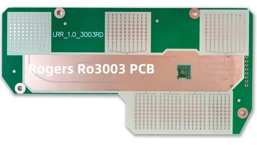
For cutting-edge communication networks like 5G and future technologies, even more specialized materials may be required:
| Property | Rogers RO3003 | Ceramic |
| Dk | 3 | 9.8-10.2 |
| Df | 0.001 | 0.0001-0.0005 |
| CTE (ppm/°C) | 17 in X,Y | 5.5-7.1 |
| Cost | Very High | Extremely High |
Balancing Performance and Cost
Hybrid Designs
To optimize both performance and cost, many PCB designers opt for hybrid designs:
- Use high-performance materials only for critical high-frequency sections
- Employ standard FR-4 for low-frequency or non-critical areas
- Implement multi-layer designs with mixed materials
Material Selection Strategy
- Identify the frequency range and critical performance parameters for the application
- Determine the production volume and budget constraints
- Consider environmental factors (temperature, humidity, etc.)
- Evaluate available materials based on electrical properties and cost
- Prototype and test with different material combinations
- Optimize the design based on test results and cost analysis
Case Studies
Case Study 1: 4G LTE Base Station PCB
Requirements:
- Frequency range: 700 MHz to 2.6 GHz
- High reliability and thermal stability
- Cost-sensitive due to large-scale deployment
Solution:
- Hybrid design using Rogers RO4350B for critical RF sections
- FR-4 for low-frequency and digital sections
- 8-layer stackup with mixed materials
Outcome:
- Achieved required RF performance
- 30% cost reduction compared to full Rogers design
- Improved thermal management due to optimized material selection
Case Study 2: 5G mmWave Small Cell PCB
Requirements:
- Frequency range: 24 GHz to 40 GHz
- Extremely low loss
- Compact design
Solution:
- Rogers RO3003 for antenna and critical mmWave sections
- PTFE-based material for feed networks
- Ceramic substrate for filters
Outcome:
- Met stringent RF performance requirements
- Achieved miniaturization goals
- Higher cost justified by performance in critical 5G infrastructure
Future Trends in PCB Materials for Communication Networks

Advanced Composites
Research is ongoing into new composite materials that combine the benefits of different substrates:
- Ceramic-filled PTFE for improved thermal management
- Nanomaterial-enhanced epoxies for better electrical performance
Eco-Friendly Materials
As environmental concerns grow, the industry is moving towards more sustainable PCB materials:
- Halogen-free substrates
- Biodegradable PCB materials
- Recyclable conductive materials
Smart Materials
The future may see the integration of smart materials in PCBs:
- Self-healing conductors
- Adaptive dielectrics that change properties based on environmental conditions
Conclusion
Selecting the right PCB material for communication network applications requires a careful balance of electrical performance and cost considerations. As technology advances, the demand for high-performance, cost-effective PCB materials continues to grow. By understanding the properties of various materials and employing strategic design approaches, engineers can create optimal solutions that meet both technical requirements and budgetary constraints.
The future of PCB materials in the communication network field looks promising, with ongoing research into advanced composites, eco-friendly options, and smart materials. As these innovations come to fruition, they will undoubtedly reshape the landscape of PCB design and manufacturing, enabling even more powerful and efficient communication networks.
FAQ
Q1: What is the most important electrical property to consider when selecting PCB materials for high-frequency applications?
A1: For high-frequency applications, the most critical electrical property is typically the dissipation factor (Df) or loss tangent. A lower Df value indicates less signal loss, which is crucial for maintaining signal integrity at high frequencies. However, the dielectric constant (Dk) is also very important for impedance control and signal propagation speed.
Q2: Can I use FR-4 for all my PCB designs to keep costs low?
A2: While FR-4 is a cost-effective and versatile material suitable for many applications, it may not be appropriate for all designs, especially those involving high frequencies (generally above 1 GHz) or requiring very low loss. For high-frequency or high-performance applications, more advanced materials like Rogers or PTFE-based substrates may be necessary to meet electrical performance requirements.
Q3: How does the choice of PCB material affect the manufacturing process?
A3: Different PCB materials have varying processing requirements. For example, PTFE-based materials often require special handling and processing techniques due to their soft nature and high melting point. Ceramic substrates may need specialized cutting and drilling processes. These factors can affect manufacturing time, complexity, and cost. Standard materials like FR-4 are generally easier and cheaper to process.
Q4: Are there any environmental considerations when selecting PCB materials?
A4: Yes, environmental factors are becoming increasingly important in PCB material selection. Some considerations include:
- Halogen-free materials to reduce environmental impact
- RoHS (Restriction of Hazardous Substances) compliance
- Recyclability and end-of-life disposal
- Energy efficiency in the manufacturing process
Q5: How do I determine if a hybrid material approach is suitable for my PCB design?
A5: A hybrid material approach may be suitable if your PCB design has distinct sections with different performance requirements. Consider a hybrid approach if:
- Your design has both high-frequency and low-frequency sections
- Only specific areas require high-performance materials
- You need to balance cost and performance
- There are significant differences in thermal management requirements across the board
Evaluate the performance requirements of each section of your PCB and consider using high-performance materials only where necessary to optimize both cost and performance.