A jumper wire is a conductive connector used to join two points in an electronic circuit on a printed circuit board (PCB). Jumper wires act as a shortcut to avoid having to route printed metal traces on the PCB to make connections between distant pads or traces. They are also used to temporarily bypass components or reroute signals during circuit prototyping or testing.
On PCBs, jumper wires allow signals in a circuit to be conveniently bridged without the layout effort of etching multiple PCB layers when routing dense designs. This article provides a detailed overview of various types of jumper wires used in PCBs and their applications.
Types of Jumper Wires
Jumper wires come in several configurations best suited for particular use cases:
Solid Copper Jumpers
A solid copper wire forms the simplest jumper connection between PCB points. Simple copper wire cut to size and soldered to pad connections serves adequately to bridge short jumper links up to an inch or less. Round or square cross-section solid copper magnet wire is commonly used. The thickness ranges from 18 AWG to 26 AWG.
Solid copper wire PCB jumpers
Stranded Jumpers
Stranded jumpers use multiple thin copper wire strands twisted or braided together to form a thicker cable jumper. Stranded wires provide flexibility easing routing through cramped layouts and installation across solder terminals. Common configurations employ stranded 22 AWG – 30 AWG jumper sets. Flux-core solder wicking assistsstranded jumpers’ solderability.

Braided flexible stranded copper wire jumper
Insulated Wire Jumpers
Insulated solid core or stranded copper wire jumpers jacketed with plastic, rubber or lacquer coatings prevent accidental short circuits to nearby pads or board features during jumper installation in complex, density PCB designs. The insulation electrically isolates the conductive core. Heat shrink tubing also protects jumper segments. Insulation colors help visually trace custom jumpers across boards.
PVC-insulated solid copper jumper wire above PCB
Preformed Jumpers
Pre-shaped jumper wires are molded into particular shapes using plastic or nylon sleeves between the endpoints allowing installation directly above components or around obstacles on crowded PCB boards without interference. By providing precisely defined stand-off heights and custom shapes conforming to circuit layouts, preformed jumpers offer reliability combined with adaptability across circuit boards.
Preformed jumper with stand-offs clearing nearby capacitors during installation
Ribbon Cable Jumpers
Using ribbon cable as jumpers on PCBs provides multiple signal connections in parallel. The flat flexible ribbon style jumper can integrate bulk wire tracking between connectors and cable assemblies laid conveniently across PCB sections with easy individual wire access. Ribbon jumper assemblies may interface external low-voltage differential signaling (LVDS) displays, keypads or cable harnesses across boards.
Rigid-Flex PCB Jumpers
Rigid-flex PCBs utilize flexible PCB extensions with embedded thin copper traces to structurally interface separate rigid PCB assemblies eliminating wired jumpers. The integrated flex jumpers folded tightly or contoured enable 3D compaction joining multilayer boards internally across devices eliminating external cabling while conducting signals reliably through flat flex bends without distortions.
PCB Jumper Wire Applications
Jumper wires satisfy diverse connectivity requirements across various kinds of PCBs:
Prototyping
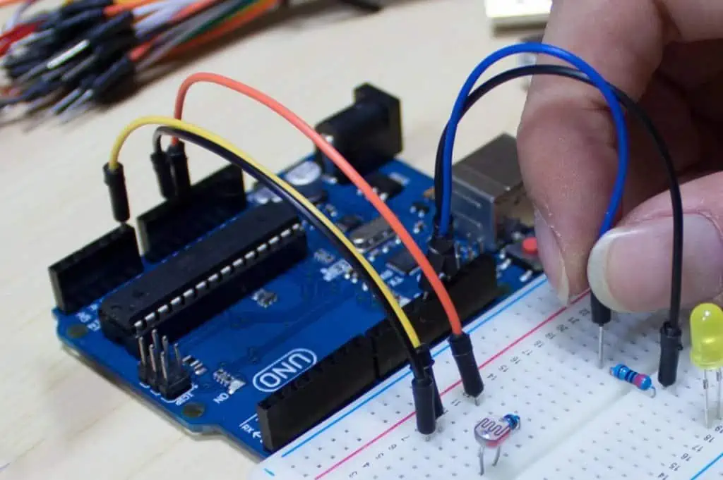
Breadboards extensively use jumper wires allowing designers to conveniently bridge components and ICs laid out temporarily to validate circuit concepts without finalized PCBs. Solid core and stranded jumpers of easily customized lengths facilitate routine reconfigurations as designs evolve through iterative testing before PCB fabrication. Prefabricated jumper sets simplify prototyping.
Circuit Modifications
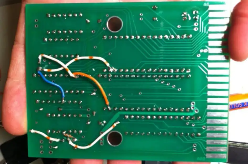
On existing PCBs, jumper wires bypass components or reroute signals during circuit modifications or corrections. Removed links are bridged or alternate board connections established for validating upgrades. Insulated jumpers prevent short circuit mishaps across increasingly congested boards. Stranded jumpers handle frequent alterations as circuits morph across multiple PCB revisions.
Density Constraints
Interconnecting distant terminals across complex high density PCBs like GPS receivers avoids extensive routing across multilayers when jumpers shortcut pads spaced far apart. Direct fly-over jumper links simplify layouts in dense designs. Right-angle jumpers clear components when bridging tight spaces. Stand-off spacers provide proper clearances.
Shield Jumpers
Solutions requiring careful impedance control at high frequencies utilize coaxial or twisted pair cables as shielded jumpers to contain electromagnetic interference (EMI). Miniature surface mount (SMT) coaxial connectors solder with adjacent ground vias suppress noise injection in multi-layer boards. Ferrite beads aid isolation.
Programming Headers
Specialized application boards may employ dual-row male pin headers as programming interfaces allowing temporary interfacing with external electronic modules or cables to update firmware or modify settings through serial data connections bridged using female-to-female jumper wires. Right-angle pin headers conserve space.
Test Points
Onboards lacking test points utilize jumper wires to sample internal signals by splicing connections onto nodes otherwise inaccessible without drilling holes on multilayer boards. Rigid tips of test probe jumpers securely latch onto solder pads, vias or component leads to non-invasively monitor waveforms for debugging firmware or diagnosing faults.
Best Practices When Using PCB Jumpers
Follow these guidelines to employ jumpers effectively while avoiding common mishaps:
- Use stranded wires offering flexibility for alterations
- Keep conductors short limiting parasitic inductance
- Define schematics/layouts clearly highlighting jumpers
- Insulate wires preventing accidental shorts
- Install spacers when bridging tall components
- Shield noisy or susceptible high-frequency paths
- Secure wires against vibration failures
- Logically label custom jumpers connections
- Limit current levels for thinner gauge wires
Advantages of Jumper Wires for PCBs
Jumper wires offer multiple benefits for connecting points on printed circuit boards:
Simplicity
Jumper wires facilitate rapid connections between existing PCB pads bypassing complex multilayer routing. Prefabricated jumper sets quicken prototyping iterations.
Adaptability
Flexible jumpers allow adjustments as design requirements evolve across future board spins. Stranded wires make alterations easier by avoiding cracked joints or damaging rigid traces.
Space Savings
Direct fly-over jumpers conserve routing real estate in cramped layouts by circumventing the need to accommodate tracing channels on all layers during multilayer PCB fabrication.
Reliability
Short jumper wire links avoid issues like opens or electrical noise compared to tiny width PCB traces spanning larger distances across boards prone to damage. Minimal solder joints also enhance dependability.
Reconfigurability
Jumpers permit customizable connectivity only finalized post-fabrication allowing designers experimenting with schemes unforeseen during CAD PCB layout stages as additional functionality gets incorporated across boards.
Economy
Supplemental jumpers mitigate complete PCB respins whenever minor circuit changes emerge saving time and costs. Jumpers also simplify specialized connectivity demands tailored per end-application without elaborate custom routing.
Design Simplicity
Using jumper wires keeps multilayer PCB stackups simpler by reducing layer count needs with fewer traces since jumpers bridge connections directly sans dedicated routing. This avoids intricate impedance tuning.
Disadvantages of Jumper Wires for PCBs
However, PCB jumper wires also come with some downsides:
Clutter
Excess jumpers crisscrossing a PCB board appears messy complicating visual inspection and physical access during rework or manual assembly especially on double-sided boards. Insulation sleeving colors help identify custom jumpers.
EMI Susceptibility
Lengthy unshielded jumper wires act as antennas injecting unwanted external electromagnet noise into sensitive circuits lacking proper guarding traces or ground isolation. This risks signal integrity issues on boards lacking proper stackup shielding.
Reliability Concerns
Mechanical stress across soldered joints or copper wire fatigue due to perpetual vibration in industrial environments risks intermittent failures over prolonged deployment durations compared to integrated PCB traces or flex circuits. Periodic inspection for cold joints or broken leads is necessary.
Switching Noise
High frequency jumper links exceeding mere inches undergo impedance mismatches potentially injecting reflections. Excessive length risks ground bounce or crossover ringing across jumper wire stubs degrading signal quality in multi-GHz circuits. Terminations may become necessary.
Assembly Issues
Hand soldering jumper wires proves trickier as PCB complexity increases due to tight clearances raising chances of short circuits or bridging solder between closely spaced surface mount device (SMD) pads when integrating supplemental jumpers across populated boards using manual rework stations.
Comparison Between PCB Traces Vs. Jumper Wires
| Parameter | PCB Traces | Jumper Wires |
|---|---|---|
| Path Lengths | Unlimited routing | Short distance links |
| Flexibility | Fixed routing | Adjustable terminations |
| Impedances | Precisely controlled | Hard to characterize |
| Switching Speeds | Multi-Gbps support | Limited to lower frequencies |
| Integration Scope | Entire PCB conductive network | Localized bridges |
| Directional Changes | Any angle | Limited without conductors kinking |
| Inductance | Lower | Increased due to wire loops |
| Parasitic Capacitance | Higher at PCB dielectric-copper interface | Lower in air medium |
| Noise Susceptibility | Guard rings and ground planes aid shielding | More prone to external interference |
| Current Capacity | High for thick copper layers | Thinner wires impose limits |
| Design Finality | Fixed layout after fabrication | Adjustable during use |
| Cost Factors | High initial PCB fabrication expenses | Low supplementary jumper wire costs |
In summary, while jumper wires adequately serve simpler connectivity needs, accommodating high-complexity multi-Gbps transfers across large boards requires precision routing to exacting impedance specifications only feasible through integral PCB metallization layers. Supplementary jumpers handle secondary localized connections.
Future PCB Jumper Wire Trends
Emerging jumper wire technologies help address existing capabilities regarding flexibility, speed and integration:
Active Optical Cables
Optical fibers replace copper jumpers for achieving high-bitrate low-loss links across backplanes. Miniaturized vertical-cavity surface-emitting lasers (VCSEL) and photodiodes integrated using chip-scale packaging techniques enable board-level optical interconnect bridges.
Carbon Nanotube (CNT) Conductors
CNT wires with high conductivity and current capacity improve jumper links for power delivery. Low inductance assists RF performance. The inherent durability surpasses copper becoming vital in aerospace systems.
Graphene Jumpers
Graphene films screen-printed onto flexible substrates that planarize onto surfaces will replace rigid jumpers. The excellent conductivity minimizes losses across folded graphene junctions. Easily customizabled graphene jumpers printed directly onto rigid or conformal surfaces become feasible.
Active ICs
Integrating tiny ICs like signal buffer/retimers using chiplets directly onto jumper wire assemblies boosts signal integrity when bridging longer traces or off-board cabling in high-speed serial links. Termination resistor chiplets also assist impedance matching.
Programmable Jumpers
Electronically switchable conductors utilizing micro-electromechanical (MEMS) actuators modify jumper connectivity. This allows changing board interconnect schemes dynamically through software reconfigurations as system requirements change eliminating manual jumper wire adjustments.
Conclusion
Jumper wires continue serving diverse connectivity demands across prototype and production PCBs thanks to simplicity and customizability despite limitations in supported distances, operating frequencies and integration challenges. Judicious utilization balancing impedance control, noise and assembly factors helps maximize utility. Moving forward, emerging jumper technologies will address existing constraints related to performance, reconfigurability and integration.
Frequently Asked Questions
How are jumper wire lengths calculated?
Jumper lengths equal the linear distance between connecting terminals plus any vertical rise above tallest components or PCB features along the bridged path. Right-angle connections require defining both horizontal and height spans to reach elevated board targets allowing safe jumper installation preventing short circuits. Extra tolerance additionally cushions links stretching during usage.
What gauge jumper wire connects GPIO pins?
General-purpose input/output (GPIO) pin interfacing requires minimum 22 AWG jumper wires to safely carry related currents while keeping inductance lower for better high frequency response during GPIO voltage transitions necessary to prevent signal integrity issues. Thinner 26-30 AWG works for low power GPIO banks. Stranded wires enhance flexibility.
How to connect ribbon cable jumper to header pins?
Ribbon cable jumper connections onto header pin rows is best accomplished by carefully aligning the ends across both rows before tightly crimping down insulation displacement connectors. This pierces the insulation allowing the flattened ribbon wire strands to make contact with the underlying male header pins eliminating tedious hand soldering. Strain relief backings prevent cable flex damage.
Why are coaxial cables used for shielded jumpers?
The coaxial construction offers excellent noise immunity by providing constant impedance low inductance signal conductor paths where the central signal core wire gets thoroughly shielded against external electromagnetic interference along the entire shielded jumper wire length using the outer grounded braided metal mesh or metallic foil layer separation by a dielectric insulator. This prevents crosstalk issues.
What safety precautions should be taken when using jumper wires?
It is critical to prevent short circuits during jumper installation across crowded PCB assemblies through steps like using insulated wires, installing wire spacers, securing wires against accidental movement, safely routing wires avoiding nearby board features, ensuring adequate insulation thickness for voltage isolation, proper wire current ratings, checking for exposed conductors potentially contacting pads, verifying broken leads etc. This avoids catastrophic failures.