In the ever-evolving world of electronics manufacturing, efficiency and reliability are paramount. One technology that has gained significant traction in recent years is Pin-in-Paste (PIP), also known as Through-Hole Reflow (THR) or Intrusive Reflow Soldering (IRS). This innovative approach combines the strengths of through-hole technology with the efficiency of surface mount assembly processes. In this comprehensive article, we will explore the intricacies of Pin-in-Paste technology, its applications, advantages, challenges, and its impact on the electronics manufacturing industry.
Understanding Pin-in-Paste Technology
Definition and Basic Principles
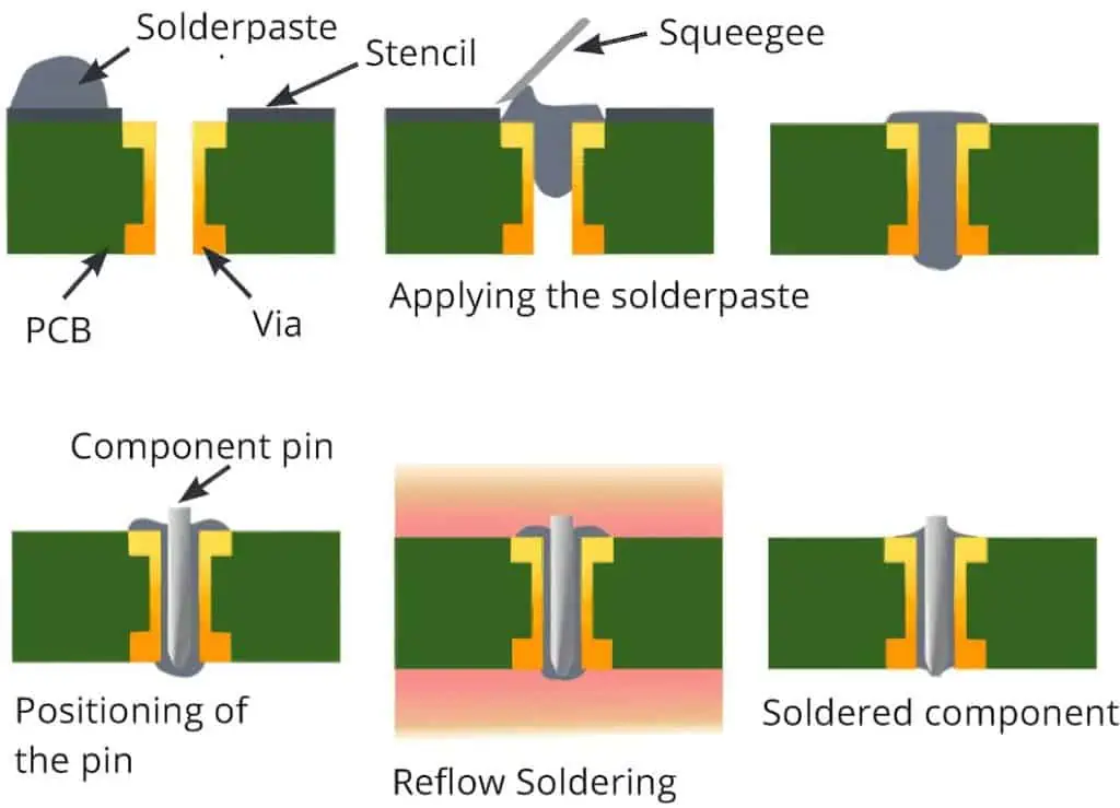
Pin-in-Paste technology is a soldering process that allows through-hole components to be soldered using the same reflow process as surface mount components. This method involves printing solder paste into and around through-holes on a printed circuit board (PCB), inserting through-hole components, and then passing the entire assembly through a reflow oven.
Key Components of PIP Technology
- Solder Paste: Special formulations designed for through-hole applications
- Stencil: Custom-designed for precise paste deposition
- Pick-and-Place Equipment: For accurate component placement
- Reflow Oven: Provides controlled heating for solder melting and cooling
The PIP Process
- Solder Paste Printing: Applying paste to PCB using a stencil
- Component Placement: Inserting through-hole components into paste-filled holes
- Reflow Soldering: Passing the assembly through a reflow oven
- Cooling and Inspection: Allowing solder joints to cool and checking quality
Comparison with Traditional Soldering Methods

To better understand the position of Pin-in-Paste technology in PCB assembly, let’s compare it with other common soldering methods:
| Soldering Method | Process Speed | Component Compatibility | Thermal Stress | Solder Joint Reliability | Cost-Effectiveness |
| Pin-in-Paste (PIP) | High | Through-hole and SMT | Medium | High | High |
| Wave Soldering | Medium | Primarily through-hole | High | Medium | Medium |
| Hand Soldering | Low | All types | Low | Varies (operator-dependent) | Low |
| Selective Soldering | Medium | Through-hole | Low | High | Medium |
| Reflow Soldering (SMT) | High | Surface mount | Medium | High |
Advantages of Pin-in-Paste Technology
Increased Manufacturing Efficiency
PIP allows for simultaneous soldering of through-hole and surface mount components, reducing overall production time and simplifying the assembly process.
Cost Reduction
By eliminating the need for separate wave soldering or hand soldering processes, PIP can significantly reduce equipment, labor, and energy costs.
Improved Solder Joint Quality
The controlled heating profile of reflow ovens often results in more consistent and reliable solder joints compared to wave soldering.
Enhanced Design Flexibility
PIP enables designers to freely mix through-hole and surface mount components on the same side of the PCB, offering greater layout options.
Environmentally Friendly
The PIP process typically uses less solder and flux compared to wave soldering, reducing waste and environmental impact.
Challenges and Considerations in PIP Implementation
Component Selection
Not all through-hole components are suitable for PIP. Factors such as lead length, component mass, and thermal sensitivity must be considered.
Paste Volume Calculation
Determining the correct amount of solder paste for each through-hole is crucial and can be complex for varied component types.
Stencil Design
Creating an effective stencil design is critical for proper paste deposition and requires expertise and often specialized software.
Process Parameter Optimization
Reflow profiles must be carefully optimized to ensure proper solder melting and wetting without damaging components.
Quality Control
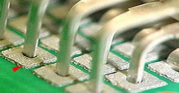
Inspection of PIP solder joints can be challenging, often requiring X-ray or other advanced inspection techniques.
Applications of Pin-in-Paste Technology
Industries Utilizing PIP
- Automotive Electronics
- Consumer Electronics
- Industrial Control Systems
- Aerospace and Defense
- Telecommunications Equipment
- Medical Devices
Specific Use Cases
- Power supply units with large through-hole capacitors
- Connectors in automotive control modules
- High-reliability aerospace circuit boards
- Mixed-technology designs in consumer electronics
- Industrial sensors with specialized through-hole components
- Medical implant devices requiring robust solder joints
Best Practices for Implementing PIP Technology
Design for PIP
- Optimize component placement for paste printing and reflow
- Consider thermal characteristics of components
- Design PCB layout to facilitate proper paste deposition
Process Optimization
- Develop and refine paste printing parameters
- Fine-tune reflow profiles for specific board designs
- Implement robust inspection and quality control measures
Material Selection
- Choose appropriate solder paste formulations
- Select compatible flux chemistries
- Ensure PCB materials can withstand reflow temperatures
Equipment Considerations
- Invest in high-precision stencil printing equipment
- Use pick-and-place machines with accurate component placement
- Select reflow ovens with precise temperature control
Training and Expertise
- Provide comprehensive training for operators and engineers
- Develop in-house expertise in PIP process optimization
- Stay updated on industry best practices and standards
Economic Impact of PIP Implementation
To illustrate the potential economic benefits of implementing Pin-in-Paste technology in a manufacturing environment, consider the following hypothetical scenario:
| Factor | Traditional Assembly | PIP Assembly |
| Annual Production Volume | 1,000,000 units | 1,000,000 units |
| Assembly Time per Unit | 15 minutes | 10 minutes |
| Labor Cost per Hour | $20 | $20 |
| Annual Labor Cost | $5,000,000 | $3,333,333 |
| Equipment Investment | $1,000,000 (Wave + Reflow) | $800,000 (Reflow Only) |
| Annual Energy Cost | $100,000 | $70,000 |
| Annual Material Cost | $2,000,000 | $1,800,000 |
| Total Annual Cost | $7,100,000 | $5,203,333 |
| Annual Savings | – | $1,896,667 |
This simplified example demonstrates how the implementation of PIP technology can lead to significant cost savings through reduced labor, equipment, energy, and material costs.
Future Trends in Pin-in-Paste Technology
Advanced Paste Formulations
Development of solder pastes with improved reflow characteristics and reliability for PIP applications.
Automation and AI Integration
Implementing machine learning algorithms for optimizing paste deposition and reflow profiles.
Enhanced Inspection Technologies
Advancements in automated optical inspection (AOI) and X-ray systems for improved quality control of PIP assemblies.
Miniaturization Challenges
Adapting PIP technology for increasingly dense and complex PCB designs.
Environmental Considerations
Further reducing the environmental impact of PIP processes through material innovations and energy efficiency improvements.
Frequently Asked Questions (FAQ)
1. What types of components are best suited for Pin-in-Paste technology?
Pin-in-Paste technology is most suitable for through-hole components that can withstand the high temperatures of reflow soldering. Ideal candidates include:
- Connectors with short pins
- Small to medium-sized capacitors and inductors
- Certain types of switches and relays
- Some semiconductor packages (e.g., TO-220)
Components that may not be suitable for PIP include:
- Large, heavy components that may fall out during reflow
- Heat-sensitive components that can’t withstand reflow temperatures
- Components with very long leads that may cause shadowing effects
The suitability of a component for PIP often depends on its specific characteristics and the overall PCB design.
2. How does Pin-in-Paste affect the reliability of solder joints compared to wave soldering?
Pin-in-Paste technology generally produces solder joints that are as reliable as, or in some cases more reliable than, those created by wave soldering. This is due to several factors:
- Controlled heating profile: Reflow ovens provide a more precise and consistent heating cycle compared to wave soldering, resulting in better solder wetting and fewer defects.
- Reduced thermal stress: PIP subjects components to a single heating cycle, whereas wave soldering often requires preheating followed by the wave process, potentially causing more thermal stress.
- Flux activity: The flux in solder paste remains active throughout the entire reflow process, promoting better wetting and cleaner joints.
- Void reduction: Properly optimized PIP processes can result in fewer voids in the solder joints compared to wave soldering.
However, the reliability of PIP solder joints can be affected by factors such as paste volume, component characteristics, and reflow profile optimization. Proper process control and design considerations are crucial for achieving high reliability.
3. What are the main challenges in transitioning from wave soldering to Pin-in-Paste?
Transitioning from wave soldering to Pin-in-Paste can present several challenges:
- Process knowledge: Developing expertise in PIP-specific aspects such as paste volume calculation and stencil design.
- Equipment investment: Acquiring or upgrading to suitable stencil printing and reflow equipment.
- Design modifications: Adapting PCB layouts and component choices to suit PIP requirements.
- Quality control: Implementing new inspection methods suitable for PIP assemblies.
- Material selection: Choosing appropriate solder pastes and flux formulations for PIP.
- Thermal management: Ensuring all components can withstand reflow temperatures.
- Training: Educating staff on new processes and best practices.
- Process optimization: Fine-tuning parameters for consistent, high-quality results.
Overcoming these challenges often requires a systematic approach, investment in resources, and a commitment to continuous improvement.
4. How does Pin-in-Paste technology impact the overall cost of PCB assembly?
Pin-in-Paste technology can significantly impact the overall cost of PCB assembly in several ways:
- Reduced equipment needs: Eliminating the need for separate wave soldering equipment can lower capital investment and maintenance costs.
- Increased throughput: PIP allows for simultaneous soldering of through-hole and SMT components, potentially increasing production speed.
- Labor savings: The more automated PIP process typically requires less manual intervention compared to wave or hand soldering.
- Material efficiency: PIP often uses less solder and flux compared to wave soldering, reducing material costs.
- Energy savings: Reflow ovens used in PIP are generally more energy-efficient than wave soldering machines.
- Improved yield: With proper implementation, PIP can result in fewer defects, reducing rework and scrap costs.
- Simplified logistics: Combining through-hole and SMT assembly steps can streamline production flow and reduce work-in-progress inventory.
While there may be initial costs associated with transitioning to PIP, many manufacturers find that the long-term cost savings outweigh the initial investment, especially for high-volume production.
5. Are there any limitations to the complexity of PCB designs when using Pin-in-Paste?
While Pin-in-Paste technology offers many advantages, it does have some limitations when it comes to PCB design complexity:
- Component density: Very high-density designs may be challenging due to the space required for paste deposition around through-holes.
- Component mix: Boards with a wide variety of through-hole component sizes and types can be difficult to optimize for PIP.
- Thermal considerations: Complex designs with heat-sensitive components near large through-hole parts may require careful thermal management.
- PCB thickness: Very thick boards may be challenging due to the need for sufficient paste volume to fill the holes.
- Double-sided assembly: While possible, PIP can be more challenging for boards requiring through-hole components on both sides.
- High-power components: Large, high-power through-hole components may not be suitable for PIP due to their mass and thermal requirements.
- Fine-pitch components: Combining very fine-pitch SMT components with PIP can be challenging due to stencil design limitations.
Despite these limitations, many complex designs can still be successfully implemented using PIP with careful planning and process optimization. In some cases, a hybrid approach combining PIP with selective or wave soldering may be used for very complex assemblies.