Introduction
In the world of DIY electronics and rapid prototyping, the ability to produce custom Printed Circuit Boards (PCBs) quickly and cost-effectively is invaluable. One innovative approach that has gained popularity among hobbyists and small-scale manufacturers is modding an inkjet printer for PCB production. This article will explore the process, benefits, and challenges of converting a standard inkjet printer into a PCB manufacturing tool.
Understanding the Basics
What is PCB Production?
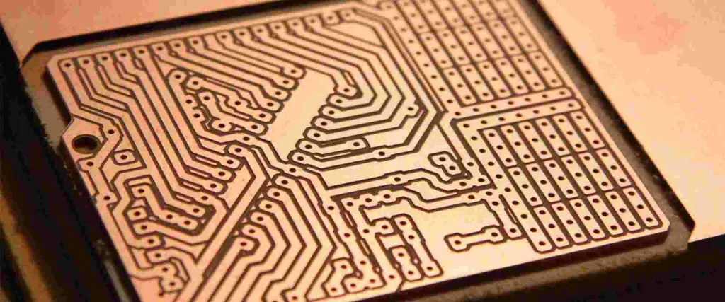
PCB production is the process of creating circuit boards that mechanically support and electrically connect electronic components using conductive tracks, pads, and other features etched from copper sheets laminated onto a non-conductive substrate.
Traditional PCB Production Methods
Traditional PCB production methods include:
The Inkjet PCB Production Method
The inkjet PCB production method involves using a modified inkjet printer to directly print resist patterns onto copper-clad boards, which are then etched to create the final PCB.

Why Mod an Inkjet for PCB Production?

Advantages
- Cost-effective for small-scale production
- Rapid prototyping capabilities
- Accessibility for hobbyists and small businesses
- Customization potential
- Environmentally friendly (less waste)
Limitations
- Limited resolution compared to professional methods
- Size constraints based on printer dimensions
- Not suitable for high-volume production
- Potential for inconsistent results
Choosing the Right Inkjet Printer
Printer Selection Criteria
When selecting an inkjet printer for PCB production, consider the following factors:
- Print resolution
- Ink type compatibility
- Paper feed mechanism
- Printer age and availability of parts
- Cost
Recommended Printer Models
| Printer Model | Resolution (dpi) | Ink Compatibility | Paper Feed | Estimated Cost ($) |
|---|---|---|---|---|
| Epson Stylus C88 | 5760 x 1440 | Pigment | Rear | 150-200 |
| Canon PIXMA iP7220 | 9600 x 2400 | Dye/Pigment | Rear/Front | 100-150 |
| HP Deskjet 1000 | 1200 x 1200 | Dye | Rear | 50-100 |
| Brother MFC-J470DW | 6000 x 1200 | Dye/Pigment | Rear/Front | 80-130 |
The Modding Process
Step 1: Disassembling the Printer
- Remove the outer casing
- Identify key components (print head, ink cartridges, paper feed mechanism)
- Document the disassembly process for reassembly
Step 2: Modifying the Paper Feed Mechanism
- Remove or adjust paper sensors
- Modify the paper tray to accommodate PCB substrates
- Adjust roller tension for thicker materials
Step 3: Adapting the Print Head
- Clean the print head thoroughly
- Modify ink channels for conductive ink (if necessary)
- Adjust print head height for PCB thickness
Step 4: Ink System Modifications
- Clean ink cartridges or replace with refillable options
- Prepare conductive ink or etchant resist ink
- Modify ink delivery system if needed
Step 5: Software and Firmware Adjustments
- Install custom firmware (if available)
- Configure printer driver settings for PCB production
- Set up appropriate design software
Step 6: Reassembly and Testing
- Carefully reassemble the modified printer
- Conduct test prints on paper
- Calibrate and fine-tune settings
Ink and Materials
Conductive Inks
| Ink Type | Conductivity (Ω/sq) | Curing Method | Cost per 100ml ($) |
|---|---|---|---|
| Silver nanoparticle | 0.01 – 0.1 | Heat/UV | 200-500 |
| Carbon-based | 10 – 100 | Air dry | 50-150 |
| Copper-based | 0.1 – 1 | Chemical/Heat | 100-300 |
| Polymer-based | 1 – 10 | Heat | 150-250 |
Etchant Resist Inks
- UV-curable inks
- Solvent-resistant inks
- Wax-based inks
PCB Substrates
- FR-4 (standard fiberglass)
- FR-1 (paper-based phenolic)
- Flexible substrates (Kapton, PET)
Printing Process
Preparing the Design
- Create PCB layout using CAD software
- Mirror the design for correct orientation
- Adjust design for printer resolution limitations
Printer Setup
- Load appropriate ink
- Calibrate print head height
- Set paper type and quality settings
Printing the PCB
- Clean and prepare the copper-clad board
- Load the board into the modified printer
- Print the resist pattern
- Allow ink to dry completely
Post-Processing
- Etching the PCB
- Cleaning and inspecting the board
- Drilling holes (if needed)
- Applying solder mask and silkscreen (optional)
Optimizing Print Quality
Factors Affecting Print Quality
- Ink viscosity
- Print head temperature
- Substrate surface preparation
- Environmental conditions (temperature, humidity)
Troubleshooting Common Issues
| Issue | Possible Cause | Solution |
|---|---|---|
| Poor adhesion | Dirty substrate | Clean thoroughly with isopropyl alcohol |
| Inconsistent lines | Clogged nozzles | Clean print head, adjust ink flow |
| Misaligned layers | Improper calibration | Recalibrate printer, check design alignment |
| Smudging | Wet ink | Increase drying time, adjust ink properties |
Maintenance and Upkeep
Regular Maintenance Tasks
- Clean print head and nozzles
- Check and replace ink as needed
- Lubricate moving parts
- Update firmware and software
Longevity Considerations
- Use high-quality components
- Store printer in a clean, dry environment
- Perform regular test prints
- Keep spare parts on hand
Advanced Techniques
Multi-Layer PCB Production
- Align layers using registration marks
- Use different inks for each layer
- Implement via-plating techniques
Fine-Pitch and SMD Components
- Optimize printer resolution
- Use specialized fine-tip print heads
- Implement solder paste printing
Flexible PCB Production
- Select appropriate flexible substrates
- Adjust ink formulation for flexibility
- Modify printer for handling flexible materials
Comparison with Other PCB Production Methods
| Method | Resolution | Cost | Speed | Complexity | Suitability |
|---|---|---|---|---|---|
| Modded Inkjet | 0.1-0.3mm | Low | Medium | Low | Prototyping, small runs |
| Photolithography | 0.1mm | Medium | Slow | High | Professional, high precision |
| CNC Milling | 0.1-0.2mm | Medium | Fast | Medium | Prototyping, small runs |
| Professional Service | <0.1mm | High | Varies | Low | Large runs, complex designs |
Future Developments
- Improved conductive inks
- Higher resolution consumer printers
- Integration with pick-and-place machines
- 3D-printed electronic components
Conclusion
Modding an inkjet printer for PCB production offers an accessible and cost-effective solution for hobbyists and small-scale manufacturers. While it has limitations compared to professional methods, the ability to rapidly prototype and produce custom PCBs in-house can be invaluable. As technology continues to advance, we can expect to see further improvements in this DIY approach to PCB manufacturing.
Frequently Asked Questions (FAQ)
1. Is modding an inkjet printer for PCB production legal?
Modding your own inkjet printer for personal use is generally legal. However, it’s important to note that this modification may void the printer’s warranty. If you plan to use the modded printer for commercial purposes, be sure to check local regulations and obtain any necessary certifications.
2. What type of ink should I use for PCB production?
For PCB production, you’ll need either conductive ink or etchant resist ink, depending on your preferred method. Conductive inks typically contain silver or copper nanoparticles, while etchant resist inks are often UV-curable or solvent-resistant. It’s crucial to choose an ink that’s compatible with your printer and substrate material.
3. How does the resolution of a modded inkjet printer compare to professional PCB production methods?
A modded inkjet printer typically achieves resolutions between 0.1mm and 0.3mm, which is suitable for many hobbyist and prototype projects. Professional PCB production methods, such as photolithography, can achieve resolutions below 0.1mm. While a modded inkjet may not match professional-grade equipment, it can produce functional PCBs for many applications.
4. Can I produce multi-layer PCBs with a modded inkjet printer?
Yes, it is possible to produce multi-layer PCBs with a modded inkjet printer, but it requires additional steps and precision. You’ll need to print each layer separately, carefully align them using registration marks, and use techniques like via-plating to connect the layers. While more challenging than single-layer boards, multi-layer production is achievable with practice and patience.
5. What are the main challenges in modding an inkjet printer for PCB production?
The main challenges include:
- Modifying the paper feed mechanism to handle rigid PCB substrates
- Adapting the ink system for conductive or resist inks
- Achieving consistent print quality and resolution
- Maintaining proper alignment for multi-layer boards
- Dealing with potential clogging issues due to specialized inks
Overcoming these challenges requires patience, experimentation, and a willingness to troubleshoot and refine your setup.