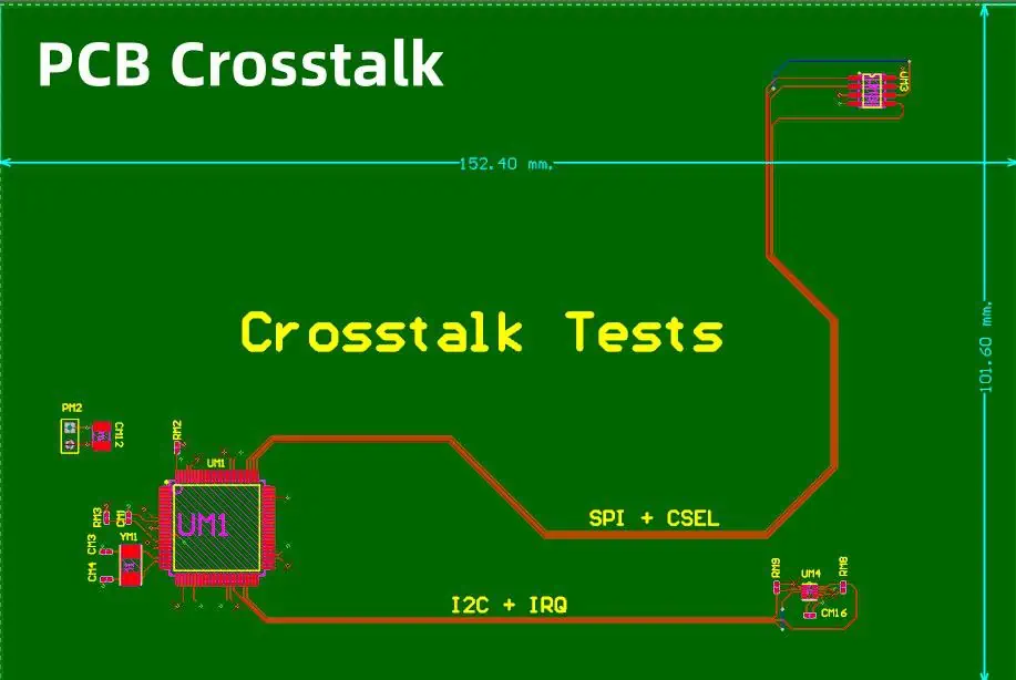
In the realm of Printed Circuit Board (PCB) design, one of the most critical challenges engineers face is managing electromagnetic interference (EMI) and signal integrity. Among these concerns, crosstalk between parallel micro-strip lines stands out as a significant issue that can compromise the performance and reliability of electronic systems. This article delves into the strategies for designing and mitigating crosstalk between two parallel micro-strip lines on PCBs, leveraging insights gained from simulation analysis.
Understanding Crosstalk in Parallel Micro-strip Lines
What is Crosstalk?
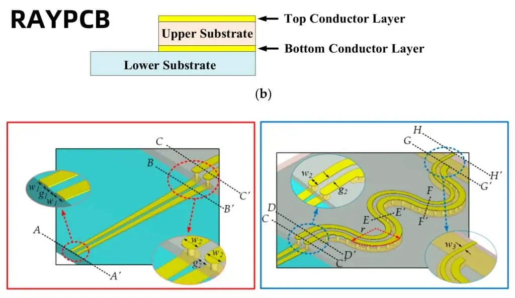
Crosstalk refers to the unintended electromagnetic coupling between adjacent signal traces on a PCB. In the case of parallel micro-strip lines, this phenomenon occurs when the electromagnetic field of one line (the aggressor) induces unwanted signals in the neighboring line (the victim).
Types of Crosstalk
- Near-end Crosstalk (NEXT): Interference measured at the same end of the transmission line as the source of the aggressor signal.
- Far-end Crosstalk (FEXT): Interference measured at the opposite end of the transmission line from the source of the aggressor signal.
Factors Influencing Crosstalk
Several factors contribute to the severity of crosstalk between parallel micro-strip lines:
- Trace spacing
- Trace length
- Signal rise/fall times
- Dielectric constant of the PCB material
- Trace width
- Signal frequency
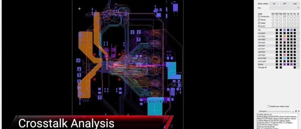
Simulation Analysis Techniques
Importance of Simulation in Crosstalk Analysis
Simulation plays a crucial role in understanding and mitigating crosstalk issues. It allows designers to:
- Predict crosstalk behavior before physical prototyping
- Optimize design parameters efficiently
- Evaluate the effectiveness of various mitigation strategies
Common Simulation Tools and Methods
- SPICE (Simulation Program with Integrated Circuit Emphasis): Ideal for time-domain analysis of crosstalk effects.
- Electromagnetic Field Solvers: Provide detailed insight into field distributions and coupling mechanisms.
- S-Parameter Analysis: Useful for frequency-domain characterization of crosstalk.
Setting Up a Simulation Model
To accurately simulate crosstalk between parallel micro-strip lines:
- Define the PCB stack-up, including layer thicknesses and material properties
- Model the micro-strip lines with appropriate dimensions and spacing
- Set up port definitions for both aggressor and victim lines
- Define simulation parameters (frequency range, time step, etc.)
- Apply appropriate boundary conditions
Strategies for Crosstalk Reduction
1. Optimizing Trace Spacing
Increasing the distance between parallel micro-strip lines is one of the most effective ways to reduce crosstalk. The relationship between spacing and crosstalk is generally inverse and non-linear.
| Trace Spacing (mils) | Relative Crosstalk (dB) |
| 5 | 0 |
| 10 | -6 |
| 20 | -12 |
| 40 | -18 |
| 80 | -24 |
2. Controlling Trace Length
Longer parallel runs increase the coupling between lines. Minimize the length of parallel segments to reduce crosstalk.
3. Managing Signal Rise/Fall Times
Slower edge rates produce less crosstalk. Consider using series termination or filtering techniques to control rise/fall times.
| Rise/Fall Time (ns) | Relative Crosstalk (%) |
| 0.1 | 100 |
| 0.5 | 60 |
| 1 | 40 |
| 2 | 25 |
| 5 | 10 |
4. Selecting Appropriate PCB Materials
Choose PCB materials with lower dielectric constants to reduce coupling between traces.
| Material | Dielectric Constant (εr) | Relative Crosstalk |
| FR-4 | 4.3-4.7 | High |
| Polyimide | 3.2-3.5 | Medium |
| PTFE | 2.1-2.5 | Low |
5. Optimizing Trace Width
Narrower traces generally produce less crosstalk but may increase resistance and heat generation.
6. Implementing Guard Traces
Placing grounded traces between signal lines can significantly reduce crosstalk.
Advanced Crosstalk Mitigation Techniques
1. Differential Signaling
Utilizing differential pairs can help cancel out common-mode noise and reduce the impact of crosstalk.
2. Layer Stacking and Routing Strategies
Orthogonal Routing
Routing adjacent layers orthogonally to each other minimizes coupling between layers.
Stripline Configuration
Embedding traces between ground planes (stripline) provides better shielding compared to micro-strip configurations.
3. Frequency-dependent Techniques
Equalization
Implementing pre-emphasis or de-emphasis can help compensate for frequency-dependent crosstalk effects.
Spread Spectrum Clocking
Reducing peak electromagnetic emissions by spreading the clock frequency can indirectly help manage crosstalk issues.
Simulation-based Optimization Process
Step 1: Initial Design and Baseline Simulation
- Create an initial PCB layout based on design requirements
- Perform baseline crosstalk simulations
- Identify problematic areas and coupling mechanisms
Step 2: Parametric Analysis
- Vary key parameters (spacing, trace width, etc.) within allowable ranges
- Run multiple simulations to understand the impact of each parameter
- Create sensitivity plots to visualize the effect of each variable
Step 3: Design Rule Formulation
Based on simulation results, formulate design rules such as:
- Minimum trace spacing for different signal types
- Maximum allowable parallel run lengths
- Recommended layer stacking configurations
Step 4: Design Iteration and Verification
- Apply optimized parameters and design rules to the PCB layout
- Re-run simulations to verify improvements
- Iterate as necessary to meet crosstalk requirements
Case Study: Optimizing a High-Speed Digital Interface
Consider a case study of a high-speed digital interface with the following initial parameters:
- Two parallel micro-strip lines on outer layer
- Trace width: 5 mils
- Trace spacing: 10 mils
- Trace length: 4 inches
- Signal rise time: 0.2 ns
- FR-4 substrate (εr = 4.5)
Initial simulation results show unacceptable levels of crosstalk. Let’s apply our optimization strategies:
Optimization Steps and Results
| Parameter | Initial Value | Optimized Value | Crosstalk Improvement |
| Trace spacing | 10 mils | 20 mils | -6 dB |
| Trace length | 4 inches | 3 inches | -2 dB |
| Rise time | 0.2 ns | 0.5 ns | -4 dB |
| Substrate material | FR-4 (εr=4.5) | Polyimide (εr=3.3) | -3 dB |
| Guard trace | None | Implemented | -8 dB |
Total crosstalk improvement: Approximately -23 dB
This case study demonstrates the significant improvements that can be achieved through simulation-based optimization of various design parameters.
Conclusion
Effectively managing crosstalk between parallel micro-strip lines on PCBs is crucial for ensuring signal integrity and overall system performance. Through careful consideration of design parameters and leveraging simulation analysis, engineers can significantly reduce crosstalk and improve the reliability of their designs.
The strategies outlined in this article, from basic techniques like optimizing trace spacing and controlling signal rise times to advanced methods such as differential signaling and guard traces, provide a comprehensive toolkit for addressing crosstalk issues. By implementing these strategies and utilizing simulation-based optimization processes, designers can create high-performance PCBs that meet the demanding requirements of modern electronic systems.
As PCB designs continue to push the boundaries of speed and density, the importance of effective crosstalk management will only grow. Staying informed about the latest simulation techniques and mitigation strategies will be essential for engineers looking to create robust and reliable electronic designs in the future.
FAQ (Frequently Asked Questions)
Q1: How does the frequency of signals affect crosstalk in parallel micro-strip lines?
A1: Higher frequency signals generally lead to increased crosstalk due to stronger electromagnetic coupling. As frequency increases, the wavelength of the signal becomes comparable to or shorter than the trace length, enhancing coupling effects. Additionally, higher frequencies typically involve faster rise/fall times, which contribute to stronger crosstalk. Designers should be especially vigilant about crosstalk mitigation techniques when working with high-frequency signals.
Q2: Can crosstalk ever be beneficial in PCB design?
A2: While crosstalk is generally considered undesirable, there are rare cases where it can be leveraged beneficially. For example, in some high-speed differential signaling applications, controlled amounts of crosstalk between the positive and negative lines of a differential pair can actually improve signal integrity by enhancing common-mode rejection. However, these cases are exceptions, and in general, minimizing crosstalk is the goal in PCB design.
Q3: How does the use of ground planes impact crosstalk between parallel micro-strip lines?
A3: Ground planes play a crucial role in managing crosstalk. They provide a low-impedance return path for signals, which helps contain the electromagnetic fields around the traces. This containment reduces the coupling between adjacent lines. Additionally, ground planes create a more controlled impedance environment, which can help maintain signal integrity. For micro-strip lines, having a solid ground plane directly beneath the signal layer is generally beneficial for crosstalk reduction.
Q4: Are there any trade-offs to consider when implementing crosstalk reduction techniques?
A4: Yes, there are several trade-offs to consider:
- Increased spacing between traces reduces crosstalk but consumes more PCB real estate.
- Wider trace spacing or the use of guard traces may require additional PCB layers, increasing cost.
- Slowing down edge rates reduces crosstalk but may impact system performance in high-speed designs.
- Using materials with lower dielectric constants can reduce crosstalk but may increase cost or present manufacturing challenges. Designers must balance these factors against performance requirements and design constraints.
Q5: How accurate are simulation results compared to real-world measurements of crosstalk?
A5: While simulation tools have become increasingly sophisticated and accurate, there can still be discrepancies between simulated results and real-world measurements. Factors contributing to these differences include:
- Idealized models used in simulations versus real-world manufacturing variations.
- Simplified material models that may not capture all frequency-dependent behaviors.
- Environmental factors not accounted for in simulations (e.g., temperature variations, external EMI).
- Measurement setup and instrumentation limitations in real-world testing.
To mitigate these discrepancies, it’s important to:
- Use accurate and detailed models in simulations.
- Apply appropriate safety margins to simulation results.
- Validate simulation results with prototypes and measurements when possible.
- Continuously refine simulation models based on measured data.