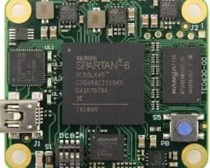
Fine-pitch PCB assembly is a critical process in the electronics manufacturing industry, enabling the production of smaller, more complex, and highly efficient electronic devices. As technology advances, the demand for miniaturization and increased functionality in electronic products continues to grow. This article delves into the intricacies of fine-pitch PCB assembly, exploring the challenges, techniques, and best practices that ensure successful outcomes in this demanding field.
What is Fine-Pitch PCB Assembly?
Fine-pitch PCB assembly refers to the process of mounting components with very small lead spacing on printed circuit boards. Typically, fine-pitch components have lead spacings of 0.5 mm or less, pushing the boundaries of traditional PCB assembly techniques.
Evolution of PCB Assembly
To understand the significance of fine-pitch assembly, it’s essential to look at the evolution of PCB assembly:
| Era | Lead Pitch | Typical Components |
| 1970s-1980s | >2.54 mm | Through-hole components |
| 1990s | 1.27-2.54 mm | Early surface-mount devices (SMDs) |
| 2000s | 0.5-1.27 mm | Fine-pitch SMDs |
| 2010s-Present | <0.5 mm | Ultra-fine pitch, BGAs, QFNs |
This progression towards finer pitches has been driven by the need for higher component density, improved performance, and reduced device sizes.
Challenges in Fine-Pitch PCB Assembly

1. Component Placement Accuracy
One of the primary challenges in fine-pitch assembly is achieving precise component placement. As lead pitches decrease, the margin for error becomes increasingly small.
Factors Affecting Placement Accuracy:
- Pick-and-place machine precision
- Component size and weight
- PCB warpage
- Thermal expansion coefficients
2. Solder Paste Deposition
Accurate solder paste deposition is crucial for successful fine-pitch assembly. Challenges include:
- Controlling solder paste volume
- Maintaining consistent paste height
- Avoiding solder bridges between adjacent pads
3. Reflow Process Control
The reflow soldering process becomes more critical with fine-pitch components. Key challenges include:
- Achieving uniform heating across the PCB
- Managing thermal profiles for different component types
- Preventing component shifting during reflow
4. Inspection and Quality Control
Detecting defects in fine-pitch assemblies requires advanced inspection techniques:
- Limitations of visual inspection
- Need for automated optical inspection (AOI) systems
- X-ray inspection for hidden solder joints (e.g., BGAs)
Advanced Techniques for Fine-Pitch PCB Assembly
1. Stencil Design and Printing
Stencil design plays a crucial role in accurate solder paste deposition for fine-pitch components.
Key Considerations in Stencil Design:
| Factor | Description |
| Aperture Size | Typically 80-90% of pad size for fine-pitch components |
| Stencil Thickness | Usually 3-4 mils (0.076-0.102 mm) for fine-pitch applications |
| Aperture Shape | Customized shapes (e.g., home plate) for optimal release |
| Nano-coating | Improves paste release and reduces bridging |
2. Advanced Pick-and-Place Technologies
Modern pick-and-place machines incorporate several technologies to improve accuracy:
- Vision systems for component alignment
- Closed-loop feedback for placement verification
- Multi-nozzle heads for increased throughput
- Linear motors for smoother, more precise movements
3. Reflow Profiling for Fine-Pitch Components
Developing an optimal reflow profile is critical for fine-pitch assembly success.
Typical Reflow Profile Zones:
- Preheat Zone
- Soak Zone
- Reflow Zone
- Cooling Zone
Each zone must be carefully controlled to ensure proper solder joint formation without damaging sensitive components.
4. Nitrogen Reflow Atmosphere
Using a nitrogen atmosphere during reflow can provide several benefits for fine-pitch assembly:
- Improved wetting and spread of solder
- Reduced oxidation of solder joints
- Lower defect rates, especially for lead-free solders
Best Practices for Fine-Pitch PCB Assembly
1. Design for Manufacturability (DFM)
Implementing DFM principles from the outset can significantly improve the success rate of fine-pitch assemblies.
Key DFM Considerations:
- Adequate spacing between components
- Proper pad design and solder mask clearances
- Thermal relief for large ground planes
- Fiducial marks for accurate component placement
2. Process Control and Monitoring
Maintaining tight control over the assembly process is crucial for consistent results.
Critical Process Parameters to Monitor:
| Parameter | Typical Range |
| Solder Paste Temperature | 20-25°C |
| Stencil Print Pressure | 0.18-0.27 kg/cm of squeegee length |
| Print Speed | 25-100 mm/s |
| Reflow Peak Temperature | 230-250°C (for SAC305 solder) |
| Cooling Rate | 2-4°C/s |
3. Environmental Control
Maintaining a controlled environment is essential for fine-pitch assembly success.
Environmental Factors to Control:

- Temperature (typically 20-26°C)
- Humidity (30-60% RH)
- Electrostatic discharge (ESD) protection
- Airborne particulate levels
4. Training and Skill Development
Investing in operator training and skill development is crucial for achieving consistent results in fine-pitch assembly.
Key Training Areas:
- Proper handling of fine-pitch components
- Visual inspection techniques
- Process control and troubleshooting
- Equipment maintenance and calibration
Advanced Inspection Techniques for Fine-Pitch Assemblies
1. Automated Optical Inspection (AOI)
AOI systems use high-resolution cameras and advanced image processing algorithms to detect defects in fine-pitch assemblies.
Common Defects Detected by AOI:
- Component misalignment
- Solder bridges
- Insufficient solder
- Missing components
2. X-ray Inspection
X-ray inspection is particularly useful for inspecting hidden solder joints, such as those found in BGA packages.
Advantages of X-ray Inspection:
- Non-destructive testing
- Ability to detect voids in solder joints
- Inspection of multiple board layers
3. In-Circuit Testing (ICT)
ICT provides electrical verification of assembled PCBs, helping to catch defects that may not be visible through optical or X-ray inspection.
ICT Capabilities:
- Short circuit detection
- Open circuit detection
- Component value verification
- Functional testing of active components
Future Trends in Fine-Pitch PCB Assembly
As technology continues to evolve, several trends are shaping the future of fine-pitch PCB assembly:
1. Further Miniaturization
The drive towards smaller, more powerful devices is pushing lead pitches even lower. Some emerging technologies include:
- 01005 (0.4 x 0.2 mm) passive components
- 0.3 mm pitch BGAs
- Wafer-level chip scale packages (WLCSP)
2. Advanced Materials
New materials are being developed to address the challenges of fine-pitch assembly:
- Low-temperature solders for heat-sensitive components
- Novel flux formulations for improved wetting and cleaning
- High-reliability conformal coatings
3. Artificial Intelligence in Assembly Processes
AI and machine learning are being integrated into various aspects of the assembly process:
- Predictive maintenance for assembly equipment
- Real-time process optimization
- Defect detection and classification in inspection systems
4. Additive Manufacturing Techniques
3D printing and other additive manufacturing techniques are being explored for PCB production, potentially revolutionizing fine-pitch assembly:
- Printed electronics for flexible circuits
- Embedded components within PCB substrates
- Custom package designs for optimal performance
Conclusion
Fine-pitch PCB assembly represents the cutting edge of electronics manufacturing technology. By understanding the challenges, implementing advanced techniques, and following best practices, manufacturers can successfully navigate the complexities of fine-pitch assembly. As technology continues to evolve, staying informed about emerging trends and continuously improving processes will be key to remaining competitive in this demanding field.
Frequently Asked Questions (FAQ)
1. What is considered “fine-pitch” in PCB assembly?
Fine-pitch typically refers to components with lead spacings of 0.5 mm or less. However, the definition can vary depending on the industry and application. Some ultra-fine-pitch components may have lead spacings as small as 0.3 mm or even less.
2. How does fine-pitch assembly differ from standard PCB assembly?
Fine-pitch assembly requires higher precision in all aspects of the process, including stencil printing, component placement, and reflow soldering. It often necessitates specialized equipment, more stringent process controls, and advanced inspection techniques to ensure quality and reliability.
3. What are the most common defects in fine-pitch PCB assembly?
Common defects in fine-pitch assembly include solder bridges (shorts between adjacent pads), insufficient solder (open circuits), component misalignment, and solder balling. These defects can be more difficult to detect and correct compared to those in standard PCB assembly.
4. How can manufacturers improve their fine-pitch assembly capabilities?
Manufacturers can improve their fine-pitch assembly capabilities by investing in advanced equipment, implementing rigorous process controls, providing comprehensive training to operators, and utilizing advanced inspection techniques. Additionally, working closely with PCB designers to ensure design for manufacturability can significantly improve outcomes.
5. What future developments can we expect in fine-pitch PCB assembly?
Future developments in fine-pitch PCB assembly are likely to include further miniaturization of components, advanced materials for improved reliability, integration of artificial intelligence for process optimization, and potentially the adoption of additive manufacturing techniques for PCB production. These developments will enable even more compact and powerful electronic devices in the future.


