Planar transformers are increasingly being used on printed circuit boards (PCB) in switch mode power supplies, DC-DC converters, gate drivers and other power electronic circuits owing to their compact size, improved performance, lower cost and ease of integration.
Designing planar transformers requires following specific layout guidelines and PCB design practices to achieve the electrical parameters, minimize parasitic losses and ensure manufacturability. This article provides a comprehensive guide on designing planar transformer PCBs.
What is a Planar Transformer?

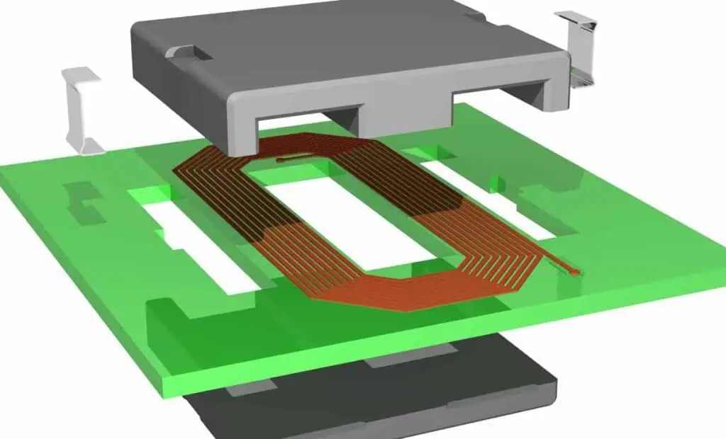
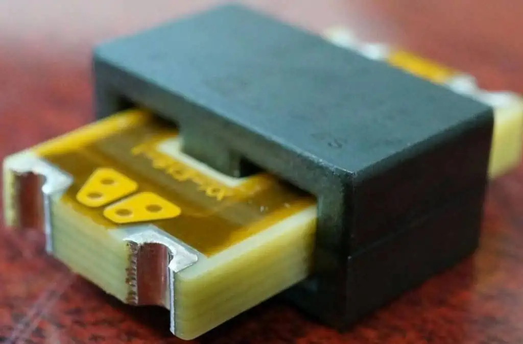
A planar transformer is a flat, low profile transformer fabricated using PCB technology. The windings are made from etched copper tracks and turns on the PCB layers. The core is realized using the PCB dielectric material itself by interleaving the winding layers.
Planar transformers provide the electrical isolation, voltage transformation and energy transfer functions of conventional wire wound transformers in a smaller surface mount device footprint. Key advantages include:
- Extremely low profile and small size
- Improved power density
- Lower leakage inductance
- Reduced parasitic capacitance
- Tightly controlled characteristics
- Simplified manufacturing
- Cost effective compared to hand wound transformers
Planar transformers are widely used in SMPS, LLC and other converters, gate drives, CM choke applications and RF impedance matching circuits.
Planar vs Conventional Wire Wound Transformer Comparison

| Parameter | Planar Transformer | Wire Wound Transformer |
|---|---|---|
| Construction | Windings etched as tracks on PCB | Windings made from insulated wires |
| Core | PCB dielectric material | Ferrite, iron alloys etc. |
| Size | Extremely compact and low profile | Larger, significant height |
| Leakage Inductance | Very low due to tight coupling | Higher due to poorer coupling |
| Parasitic Capacitance | Low as limited overlapping area | High due to more overlapping wires |
| AC Resistance | Low as wider copper tracks | Higher due to thinner winding wires |
| Turns Ratio Range | Typical 1:1 to 1:5 | Wide – 10:1 or more |
| Power Levels | Lower – less than 10W usually | Higher power handling capacity |
| Cost | Lower due to PCB process | Higher labor for hand winding |
| Integration | Excellent, embed directly on PCB | Moderate, but requires mounting |
| Repeatability | Very consistent and controlled | Poorer tolerance and unit-unit variation |
| Efficiency | >90% in well designed planar transformers | >95% in conventional transformers |
Planar Transformer Construction
Planar transformers fabricated on PCB comprise the following elements:
- Primary Winding – Made from PCB copper traces forming turns on a dedicated layer.
- Secondary Winding – Second layer with turns made using etched PCB tracks.
- Dielectric Layers – FR4 or other PCB substrate dielectrics act as insulating barrier between windings.
- Magnetic Core – The PCB dielectric layers themselves form the core of the planar transformer.
- Interconnections – Vias interconnect the ends of primary and secondary windings for circuit connections.
- Shield Layer – Additional PCB copper layer to enclose windings for EMI control.
- Encapsulation – Transformer may be encapsulated with epoxy or molding for protection.
Design Process for a Planar Transformer PCB

The typical design flow involves the following steps:
1. Define Electrical Specifications
- Required primary and secondary voltages
- Turns ratio
- Output power
- Switching frequency
- Duty cycle
- Efficiency target
- Other parameters like leakage inductance etc.
2. Select Core Material
- Choice of PCB dielectric material (FR4, Isola, Rogers, etc.)
- Number of layers in PCB stackup
- Thickness of dielectric layers
3. Calculate Number of Turns
- Determine number of primary and secondary turns to achieve turns ratio based on voltages
- Account for minimum required inductance
- Estimate effective core area
4. Estimate Conductor Thickness
- Select copper thickness/weight to handle expected load current
- Account for allowable temperature rise
5. Design Winding Layout
- Arrange turns to minimize overall area
- Ensure adequate creepage and clearance between windings
- Include shielding layer if needed
6. Size Winding Traces
- Calculate trace width and spacing to match copper thickness
- Manage leakage inductance via tight trace coupling
- Minimize parasitic capacitance between windings
7. Validate Electrical Performance
- Simulate transformer design to verify inductance, losses, impedance etc.
- Iterate to meet specifications
8. Finalize PCB Layout
- Layout board with integrated planar transformer following best practices
- Add test points for characterization
9. Test Prototype
- Fabricate prototype PCB and evaluate transformer parameters
- Correlate measurements with simulations
- Tune design if required and repeat prototype testing
The intricacies involved in each step are explained in detail in the following sections.
Selecting Core Material and Stackup
The choice of PCB dielectric material and layer stackup determines the magnetic core properties of the planar transformer:
- PCB Dielectric Type – FR4, Isola, Rogers, Arlon etc. Low loss dielectrics improve efficiency.
- Number of Layers – More layers increase primary to secondary isolation and creepage distance. 4 to 6 layers are typical.
- Core Thickness – Total thickness of dielectric layers comprising the core affects inductance.
- Dielectric Constant – Impacts achievable inductance since magnetic field lines pass through dielectric.
- Loss Tangent – Low loss tangent materials reduce eddy current losses improving efficiency.
- Z-direction Thermal Conductivity – Helps conduct heat from windings to external PCB layers.
For low power planar transformers, typically 2 oz. copper layers are used. For higher current capacity, 3 oz. or 4 oz. copper or even heavier copper up to 6 oz. can be utilized.
Calculating Number of Turns and Inductance
The number of turns required depends on the input and output voltages of the planar transformer based on the standard transformer voltage equation:
Vp / Vs = Np / Ns
Where:
Vp = Primary Voltage
Vs = Secondary Voltage
Np = Number of Primary Turns
Ns = Number of Secondary Turns
Once the turns ratio is determined, the actual number of turns can be calculated based on the area of the windings using:
L = (N^2 * A * μ) / l
Where:
L = Inductance in Henries
N = Number of turns
A = Cross sectional area of core in m^2
μ = Permeability of core
l = Magnetic path length in meters
For planar transformers, conservative inductance targets are preferred since achieving very high inductance requires large number of turns increasing size. Typical inductance values range from 1μH to 30μH for most designs.
Winding Layout Design
The winding layout arrangement determines the magnetic coupling and performance. Some layout guidelines are:
- Place windings as close as manufacturing tolerances permit for tight magnetic coupling
- Interleave or cross windings at 90 degrees for high mutual inductance
- Minimize winding layers for reduced proximity effect losses
- Keep windings compact to increase magnetic field concentration
- Maintain symmetry between windings for optimal coupling
- Surround with ground shield to contain electromagnetic fields
- Align winding axes to improve coupling and repeatability
- Place tuner components like resonating capacitors close to minimize stray interconnect inductance
Winding patterns can be interleaved, stacked, sectionalized or interwoven based on performance targets, manufacturability constraints and the number of available PCB layers.
Determining Optimal Winding Trace Dimensions
The width and spacing of the copper traces comprising the planar transformer windings must be carefully designed:
- Trace Width – Based on expected load current and allowable temperature rise. Wider traces have higher conductance.
- Trace Thickness – Depends on copper weight used. Heavier copper can carry more current.
- Trace Spacing – Controls leakage inductance. Tighter spacing reduces leakage inductance.
- Edge Spacing – Increased spacing at turns edges reduces fringing effects and improves coupling.
- Trace Length – Impacts DC resistance. Shorter length decreases losses.
- Number of Layers – More parallel layers lowers AC resistance and proximity effect.
- Fill Ratio – Ratio of total trace width to pitch should be maximized for high coupling.
- Layers Spacing – Thicker spacing between layers increases creepage distance and isolation.
Electrical simulations are used to determine the optimal trade-off between trace dimensions, leakage inductance, DC resistance and capacitance.
Simulating and Characterizing Planar Transformer Performance
Simulating the designed planar transformer is key before fabrication to verify performance against specifications and characterize parameters like:
- Turns Ratio – Verify transformation ratio between primary and secondary voltages.
- Inductance – Leakage and magnetizing inductance of both windings.
- DC Resistance – Resistance of primary and secondary windings.
- Q Factor – Quality factor determining losses.
- Leakage Fields – Fringing leakage flux between windings.
- Current Density – Validate winding trace thickness can carry maximum current loading.
- Impedance -Transformer input and output impedance at operating frequencies.
- Efficiency – Simulate core and copper losses to estimate achievable efficiency.
Any issues found during simulation can be addressed by revising the design before layout and prototype fabrication.
Layout Best Practices for Optimal Planar Transformer Performance
Careful attention must be paid to the PCB layout to realize the full performance potential of a planar transformer:
- Maintain symmetry between primary and secondary windings for good matching.
- Place windings on adjacent layers for tight magnetic coupling and low leakage fields.
- Minimize overlap between non-adjacent winding layers to reduce inter-winding capacitance.
- Use shielding layers above and below windings to reduce EMI emissions and interference.
- Surround with ground fills and voids in planes under the core area to prevent eddy current losses.
- Incorporate thermal reliefs and voids in thermal pads for proper heat dissipation from windings.
- Ensure sufficient isolation spacing between primary and secondary circuits.
- Add test points to enable characterization of transformer after fabrication.
- Keep high dv/dt traces away from the transformer area to prevent EMI coupling.
- Use staggered and multi-Via stitching to provide robust interconnections.
- Maintain adequate creepage and clearance from transformer to other components and board edges.
Simulation vs Measurement Correlation
Once the prototype PCB with integrated planar transformer is fabricated, the parameters must be measured to correlate with simulated values. Good correlation helps validate the accuracy of modeling and design process for future designs.
Differences between simulated and measured results can be due to:
- Variations in dielectric constant or loss tangent of material.
- Inaccurate estimates of trace dimensions or spacing.
- Layer registration tolerance and misalignments.
- Improper calibration or parasitic effects during measurements.
- Simplified assumptions in simulation models.
- Process defects like under etching of traces.
- Damage to windings or tracks during board handling and assembly.
The design can be fine tuned based on feedback from measured results to achieve results closer to simulations. The improved model then becomes the baseline for subsequent design iterations.
Applications of Planar Transformers

Some common applications where planar transformers provide benefits are:
- Gate Driver Circuits: Used to drive power transistors and IGBTs isolated from control electronics.
- Switch Mode Power Supplies: Small planar transformers used in DC-DC converters, LLC resonant converters, and other SMPS.
- CM Chokes: Provide common mode noise filtering while passing differential signals.
- EMI Suppression: Low leakage enables high CMRR for power line EMI filtering.
- Audio Circuits: Low profile high fidelity transformers used in headphone amplifiers and other audio applications.
- Impedance Matching: Match signal sources to transmission lines in RF circuitry.
- Voltage Translation: Voltage transformation for battery backed systems like RTCs and memory.
- Flyback Converters: Compact efficient planar transformers used in low power flyback SMPS.
- Medical Electronics: Electrical isolation required for patient safety in medical devices.
Design Challenges with Planar Transformers
Some of the common design challenges encountered with planar transformers that must be addressed are:
- Achieving sufficient inductance within the available PCB area and layers.
- Minimizing eddy current losses in windings due to high frequency AC currents.
- Reducing inter-winding capacitance leading to increased losses and EMI.
- Preventing core saturation due to DC bias current in transformer windings.
- Handling thermal rise due to resistive copper losses in windings under load.
- Containing electromagnetic interference and noise pickup or radiation.
- Providing adequate galvanic isolation between primary and secondary circuits.
- Ensuring proper impedance matching between source and load connected to transformer.
- Overcoming variations in manufacturability of tight tolerance windings across PCB fabrication shops.
Design Review Checklist
The following checklist summarizes the key points to review during the design review process for a planar transformer PCB design:
- Confirm electrical parameters like inductance, turns ratio, efficiency meet requirements.
- Verify adequate isolation spacing between primary and secondary.
- Check for sufficient creepage distance between high voltage nodes.
- Ensure trace width and copper thickness can carry maximum current loading.
- Validate adequate thermal heat sinking of windings to handle dissipated power.
- Review parasitic capacitance and leakage inductance meets target levels.
- Evaluate EMI emissions and susceptibility performance.
- Confirm mechanical spacings for manufacturing and service clearances are met.
- Check board area utilized compared to conventional discrete transformer.
- Ensure models and simulations have been correlated with measured results on prototypes.
- Review if design leverages PCB technology benefits fully compared to hand wound transformers.
- Validate design margins, deratings and analyze risks due to unit-unit variations.
Conclusion
Well designed planar transformers enable realizing the advantages of compactness, improved efficiency, lower cost, tighter tolerance and excellent integration offered by the PCB fabrication technology. However, careful modeling, analysis and layout techniques must be followed paying attention to electromagnetic, thermal and manufacturing considerations. Leveraging PCB design automation tools for analysis, verification and layout greatly simplifies creating high performance planar transformers tailored to the application needs.
Frequently Asked Questions on Designing Planar Transformers
Q1. What are the typical dielectric core materials used for planar transformer PCBs?
FR4 is commonly used due to low cost. For higher performance, RF materials like Isola, Rogers, Arlon etc. are preferable due to lower loss tangent.
Q2. How many turns should be used for planar transformer windings?
Optimal number of turns depends on required inductance and voltages. Typical range is 4-6 turns for primary and secondary to balance size and performance.
Q3. What PCB copper thickness should be used for planar transformer windings?
1 oz. or 2 oz. copper is suitable for low current designs. For higher load current handling, 3 oz., 4 oz. or thicker copper up to 6 oz. would be recommended.
Q4. What construction approaches are used for multilayer planar transformers?
Interleaved, stacked, sectionalized and interwoven winding arrangements on multiple layers are commonly used construction techniques.
Q5. How can performance differences between simulation and measurements of fabricated planar transformer be minimized?
Careful modeling of parasitics and tolerances coupled with correlation using prototype measurements helps improve simulation accuracy and achieve results closer to real performance.
