The explosive growth of wearable technology and ubiquitous computing has revolutionized how we interact with electronic devices. This transformation has brought unique challenges and opportunities in printed circuit board (PCB) design and manufacturing. This comprehensive guide explores the essential aspects of designing PCBs for wearables and ubiquitous computing applications, focusing on miniaturization, power efficiency, and reliability.
Key Design Considerations
Form Factor Constraints
Wearable devices demand extremely compact PCB designs while maintaining full functionality. The following table outlines typical form factor constraints for different wearable categories:
| Device Type | Typical PCB Size (mm) | Maximum Height (mm) | Flex/Rigid-Flex Required |
| Smartwatch | 30 x 30 | 1.6 | Optional |
| Fitness Band | 20 x 10 | 1 | Recommended |
| Smart Ring | 15 x 15 | 0.8 | Required |
| Smart Glasses | 40 x 15 | 1.2 | Required |
| Hearing Aids | 10 x 5 | 0.6 | Required |
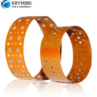
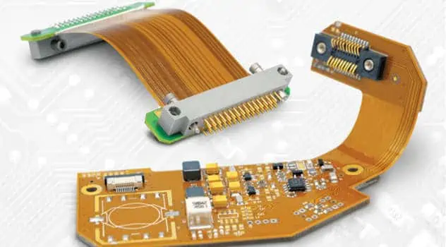
Material Selection
Substrate Materials
| Material Type | Advantages | Disadvantages | Recommended Applications |
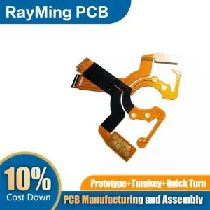
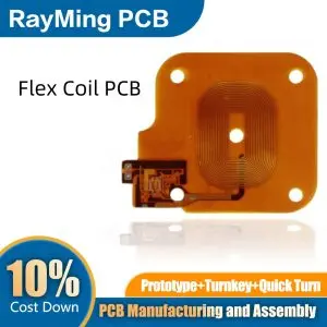
| Polyimide | High flexibility, temperature resistant | Higher cost | Flex and rigid-flex designs |
| FR-4 | Cost-effective, widely available | Limited flexibility | Rigid sections |
| PTFE | Excellent RF properties | Expensive, processing challenges | RF modules |
| LCP | Good for high-frequency, moisture resistant | Complex processing | High-frequency applications |
Power Management Optimization
Power Consumption Guidelines
Current Consumption Targets
| Function | Active Mode (mA) | Sleep Mode (µA) | Standby Mode (µA) |
| MCU | 0.5-5 | < 1 | < 0.1 |
| Sensors | 0.1-2 | < 0.5 | < 0.05 |
| Display | 5-50 | < 10 | < 1 |
| Radio | 10.-30 | < 2 | < 0.2 |
Battery Integration
Battery Technology Selection
| Battery Type | Energy Density (Wh/L) | Cycles | Best Use Case |
| Li-Po | 250-730 | 300-500 | Smartwatches |
| Li-Ion | 200-630 | 500-1500 | Larger wearables |
| Solid State | 200-500 | >1000 | Safety-critical |
| Silver-Zinc | 130-350 | 100-200 | Hearing aids |
Component Selection and Layout
Component Density Optimization
The following table provides guidelines for component density based on device type:
| Device Category | Components/cm² | Minimum Trace Width (mm) | Minimum Spacing (mm) |
| Ultra-compact | >50 | 0.075 | 0.075 |
| Compact | 30-50 | 0.1 | 0.1 |
| Standard | 20-30 | 0.125 | 0.125 |
| Low-density | <20 | 0.15 | 0.15 |
Thermal Management
Thermal Design Considerations
| Heat Source | Maximum Temperature (°C) | Cooling Strategy |
| Processor | 85 | Copper spreading |
| Battery | 45 | Thermal isolation |
| Power Management | 70 | Component spacing |
| Radio Module | 60 | Ground plane optimization |
Manufacturing and Assembly
Design for Manufacturing (DFM) Guidelines
Critical Manufacturing Parameters
| Parameter | Standard Class | High-Density Class | Ultra-High-Density Class |
| Min. Trace Width | 0.15 mm | 0.10 mm | 0.075 mm |
| Min. Via Diameter | 0.3 mm | 0.2 mm | 0.15 mm |
| Layer Count | 4.-6 | 6.-8 | 8.-12 |
| Min. BGA Pitch | 0.8 mm | 0.65 mm | 0.5 mm |
Reliability Considerations
Environmental Testing Requirements
| Test Type | Condition | Duration | Pass Criteria |
| Temperature Cycling | -40°C to +85°C | 500 cycles | No failures |
| Humidity | 85% RH at 85°C | 1000 hours | No corrosion |
| Drop Test | 1.5m drop | 26 drops | No functional failure |
| Sweat Resistance | Artificial sweat | 96 hours | No degradation |
Connectivity Solutions
Wireless Technology Selection
| Technology | Power Consumption | Range | Data Rate | Best Use Case |
| Bluetooth LE | Very Low | 10m | 2 Mbps | Personal devices |
| Wi-Fi | High | 50m | >100 Mbps | Data-intensive apps |
| NFC | Ultra-Low | 10cm | 424 Kbps | Payment systems |
| UWB | Medium | 10m | >100 Mbps | Precise location |
Sensor Integration
Common Sensor Types and Requirements
| Sensor Type | Power (mW) | I/O Interface | PCB Area (mm²) |
| Accelerometer | 0.1-1.0 | I²C/SPI | 4.-9 |
| Heart Rate | 0.5-2.0 | I²C | 9.-16 |
| Temperature | 0.01-0.1 | I²C/ADC | 2.-4 |
| Bio-impedance | 1.0-5.0 | ADC | 16-25 |
Design Verification and Testing
Test Point Strategy
Test Point Allocation
| Circuit Type | Minimum Test Points | Coverage Target | Test Method |
| Power Rails | 2 per rail | 100% | In-circuit |
| Digital I/O | 75% coverage | 90% | Boundary scan |
| Analog Signals | 100% coverage | 95% | Flying probe |
| RF Circuits | Key nodes only | 80% | Custom fixture |
Future Trends and Innovations
Emerging Technologies
| Technology | Expected Impact | Timeline | Key Benefits |
| Flexible PCBs | High | 2024-2025 | Improved conformability |
| 3D Printing | Medium | 2025-2026 | Rapid prototyping |
| Embedded Components | Very High | 2024-2027 | Size reduction |
| Biodegradable Substrates | Medium | 2026-2028 | Sustainability |
Frequently Asked Questions
1. What are the key challenges in designing PCBs for wearable devices?
The main challenges include:
- Extreme miniaturization requirements
- Power management optimization
- Heat dissipation in confined spaces
- Flexibility and durability needs
- Environmental protection requirements Each challenge requires careful consideration during the design phase and appropriate material and component selection.
2. How can battery life be optimized in wearable PCB designs?
Battery life optimization involves multiple strategies:
- Implementing efficient power management circuits
- Using low-power components and sleep modes
- Optimizing wireless communication protocols
- Careful component placement to minimize power trace lengths
- Implementing intelligent power scheduling algorithms
3. What are the most important considerations for flexible PCB designs in wearables?
Key considerations include:
- Material selection (polyimide vs. other flexible substrates)
- Bend radius limitations
- Component placement in relation to flex zones
- Strain relief design
- Layer stack-up optimization for flexibility These factors directly impact the reliability and durability of the final product.
4. How do you ensure reliability in wearable PCB designs?
Reliability is ensured through:
- Comprehensive environmental testing
- Proper component selection for the application
- Adequate protection against moisture and sweat
- Mechanical stress management
- Thermal management strategies Regular validation and testing throughout the design process is essential.
5. What emerging technologies are impacting wearable PCB design?
Several technologies are shaping the future of wearable PCBs:
- Advanced flexible and stretchable substrates
- Embedded component technologies
- 3D-printed electronics
- Novel interconnect solutions
- Biodegradable materials These technologies are enabling new form factors and applications in wearable devices.
Conclusion
The design of PCBs for wearables and ubiquitous computing represents a unique intersection of challenges and opportunities in electronic design. Success in this field requires careful attention to miniaturization, power efficiency, reliability, and manufacturability. As technology continues to evolve, designers must stay informed about new materials, components, and techniques while maintaining focus on the fundamental principles of good PCB design. The future of wearable PCB design lies in the successful integration of emerging technologies with proven design methodologies to create increasingly sophisticated and reliable devices.