Modern electronic systems are pushing the boundaries of power density, cramming more functionality into smaller spaces while demanding higher performance. At the heart of these systems lies the printed circuit board (PCB), which must not only provide electrical connectivity but also serve as a critical thermal management component. Understanding how board thickness influences power handling capabilities is essential for preventing catastrophic overheating and ensuring reliable operation across demanding applications.

The Thermal Challenge in Modern PCBs
As electronic devices become more compact and powerful, the heat generated per unit area continues to increase dramatically. Power semiconductor devices, high-frequency processors, and dense component layouts create thermal hotspots that can quickly exceed safe operating temperatures. When a PCB cannot adequately dissipate this heat, components experience reduced performance, shortened lifespan, or complete failure.
The relationship between power handling and board thickness is fundamentally rooted in thermal physics. Heat generated by components must travel through the PCB substrate to reach heat sinks, thermal vias, or the ambient environment. The efficiency of this heat transfer process directly impacts the maximum power that can be safely handled without compromising system reliability.
Understanding Heat Flow in PCB Substrates
Heat transfer in PCBs occurs primarily through conduction, following the basic principle that heat flows from hot regions to cooler ones. The rate of heat transfer depends on several factors: the thermal conductivity of the materials, the cross-sectional area available for heat flow, the temperature gradient, and the distance the heat must travel.
Board thickness plays a crucial role in this equation by affecting both the thermal resistance and the available pathways for heat dissipation. A thicker board provides more material volume to absorb and distribute heat, effectively creating a larger thermal mass that can buffer temperature spikes during transient power events.
The Physics of Thermal Resistance
Thermal resistance in a PCB can be understood using an electrical analogy, where heat flow resembles current flow and temperature differences correspond to voltage drops. The thermal resistance of a material is inversely proportional to its cross-sectional area and directly proportional to its thickness and the reciprocal of its thermal conductivity.
For a uniform material, thermal resistance equals thickness divided by the product of thermal conductivity and cross-sectional area. This relationship initially suggests that increasing thickness would increase thermal resistance, making heat transfer more difficult. However, the reality in PCB applications is more complex due to the multi-layered nature of modern boards and the distribution of heat sources and sinks.
In practice, thicker PCBs often demonstrate better thermal performance because they provide increased copper volume for heat spreading and more space for thermal management features like buried thermal vias, thick copper planes, and thermal interface materials.
Material Considerations and Thermal Properties
The substrate material significantly influences how board thickness affects thermal performance. Standard FR-4 fiberglass has relatively poor thermal conductivity (approximately 0.3 W/m·K), making it somewhat inefficient for heat conduction. However, thicker FR-4 boards can still improve thermal performance by providing more volume for copper layers and thermal vias.
High-performance applications often utilize substrates with enhanced thermal properties. Materials like aluminum-backed PCBs, ceramic substrates, or specialized thermally-enhanced laminates offer superior thermal conductivity. When combined with increased thickness, these materials can dramatically improve power handling capabilities.
Copper layers within the PCB stack-up play an equally critical role. Copper’s excellent thermal conductivity (approximately 400 W/m·K) makes it the primary heat spreading mechanism in most PCBs. Thicker boards allow for heavier copper weights and additional copper layers, creating more efficient thermal pathways throughout the board.
Heat Spreading and Distribution Benefits
One of the most significant advantages of increased board thickness is improved heat spreading capability. When a high-power component generates heat, that energy must be distributed across a larger area to prevent localized hot spots. Thicker boards provide more copper volume and additional layers that can act as heat spreaders, distributing thermal energy more evenly across the board’s surface.
This spreading effect is particularly important for power components like voltage regulators, power MOSFETs, and high-current connectors. By distributing heat over a larger area, the local temperature rise is reduced, allowing components to operate within their safe temperature limits even at higher power levels.
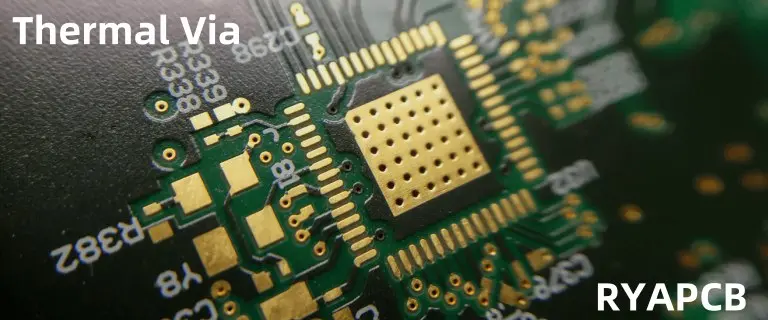
Thermal Via Design and Implementation
Thicker PCBs offer enhanced opportunities for thermal via implementation. Thermal vias are copper-filled holes that create vertical heat conduction paths between layers, allowing heat to transfer from hot components to cooler areas of the board or to external heat sinks.
In thicker boards, thermal vias can be larger in diameter and more numerous without compromising structural integrity or routing density. Additionally, the increased board thickness allows for more sophisticated via arrangements, such as via-in-pad designs or arrays of thermal vias that create highly effective heat conduction paths.
The thermal resistance of a via depends on its diameter, length, and the thermal interface between the via and the surrounding materials. Thicker boards, while requiring longer vias, can accommodate larger diameters and better thermal interfaces, often resulting in net improvements in thermal performance.
Design Strategies for Optimal Thermal Performance
Effective thermal management in thicker PCBs requires careful consideration of layer stack-up design. Dedicated thermal layers, typically implemented as solid copper planes, can be strategically positioned throughout the board stack-up to create efficient heat spreading networks. These layers should be connected through thermal vias and designed to minimize thermal bottlenecks.
Component placement becomes increasingly critical in thicker board designs. High-power components should be positioned to take advantage of thermal pathways and avoid creating thermal shadows that could trap heat. The three-dimensional nature of thicker boards allows for more sophisticated thermal routing, including the use of buried heat spreaders and internal thermal interfaces.
Copper balancing across layers also impacts thermal performance. Unbalanced copper distribution can create thermal gradients that lead to warping and mechanical stress. Thicker boards are generally more tolerant of copper imbalances, but careful design is still required to optimize thermal performance.
Trade-offs and Design Considerations
While increased board thickness generally improves thermal performance, it comes with several trade-offs that designers must consider. Thicker boards increase manufacturing costs due to longer processing times, more materials, and potentially lower yields. They also add weight and volume to the final product, which may be critical constraints in portable or aerospace applications.
Manufacturing constraints also become more challenging with increased thickness. Aspect ratios for vias become more demanding, requiring careful consideration of drill sizes and plating processes. Signal integrity can be affected by longer via lengths, potentially requiring additional design measures to maintain electrical performance.
Mechanical considerations include increased stiffness, which can be beneficial for reducing vibration-induced failures but may also increase stress concentrations at component interfaces. The coefficient of thermal expansion mismatch between the PCB and components can also become more pronounced in thicker boards, requiring careful attention to solder joint reliability.
Real-World Applications and Case Studies
High-power LED applications demonstrate the benefits of increased board thickness particularly well. LED arrays generate significant heat in small areas, and failure to manage this heat leads to rapid degradation of light output and color stability. Thick aluminum-backed PCBs or multi-layer boards with heavy copper have become standard solutions for high-performance LED systems.
Power electronics applications, including motor drives, power supplies, and electric vehicle systems, routinely utilize thick PCBs to handle high current densities. These applications often combine thick substrates with specialized thermal interface materials and external heat sinks to achieve optimal thermal performance.
Telecommunications and data center equipment represent another area where thick PCBs provide thermal advantages. High-speed processors and power amplifiers in these systems generate substantial heat loads that require sophisticated thermal management strategies, often including thick multi-layer boards with integrated thermal features.
Future Trends and Emerging Technologies
The trend toward higher power densities and more compact electronic systems continues to drive innovations in PCB thermal management. Advanced materials with enhanced thermal properties, including graphene-enhanced substrates and diamond-like carbon coatings, are being integrated into thicker board designs to push thermal performance boundaries.
Three-dimensional integration technologies are also benefiting from advances in thick board thermal management. As components are stacked vertically and integrated more densely, the ability to conduct heat through thick substrates becomes increasingly critical for system reliability.
Conclusion
Board thickness represents a fundamental design parameter that significantly influences PCB power handling capabilities. While the relationship between thickness and thermal performance is complex and application-dependent, thicker boards generally provide superior thermal management through increased thermal mass, enhanced heat spreading, and improved opportunities for thermal via implementation.
Successful thermal management in high-power PCB applications requires a holistic approach that considers material selection, layer stack-up design, component placement, and manufacturing constraints. As electronic systems continue to demand higher power densities, understanding and leveraging the thermal benefits of increased board thickness will remain essential for preventing overheating and ensuring reliable operation.
The investment in thicker PCB designs often pays dividends in improved reliability, longer component lifespans, and the ability to push system performance boundaries. For engineers working with high-power applications, careful consideration of board thickness as part of a comprehensive thermal management strategy is not just beneficial—it’s essential for success.