In PCB design, a fiducial marker is a small, rounded copper feature that serves as a reference point for automated pick-and-place assembly machines. These markers enable machine vision systems to accurately detect the PCB’s position and orientation as it moves through Surface Mount Technology (SMT) assembly lines. By comparing the PCB’s alignment with the pre-programmed orientation of components on reels, the machine can adjust part placement—including rotation—to ensure precise positioning on their designated land patterns.
Why Use Fiducial Markers?
Fiducials are a simple yet critical feature that should be incorporated into PCB designs whenever possible, particularly for square or rectangular boards. They enhance assembly accuracy and reduce misalignment errors, which is especially important for:
- High-density designs (e.g., fine-pitch components like QFPs, BGAs, or QFNs)
- High-volume production (where consistency is crucial)
Placement Guidelines
- Global Fiducials – Typically placed near the PCB corners to provide overall board alignment.
- Local Fiducials – Positioned near critical components (e.g., fine-pitch ICs) to improve placement precision for specific parts.
The choice between global and local fiducials depends on:
Component pitch (smaller pitches often require additional fiducials for accuracy)
Production volume (high-volume runs benefit from both types)
Assembler requirements (some may demand local fiducials for tight-tolerance components)

Fiducial Markers in PCB Manufacturing: Types and Critical Functions
Fiducial markers are essential reference points in PCB manufacturing that enable precise component placement during automated assembly. These copper landmarks guide pick-and-place machines by providing exact positional data, ensuring accurate alignment of surface-mount components.
Two Key Types of Fiducial Markers
- Global Fiducial Markers
- Positioned near the PCB edges to establish the board’s overall orientation.
- Help machines determine the PCB’s X-Y axis alignment and correct for any skew or misplacement when clamped.
- Critical for ensuring panel-level accuracy in high-volume production.
- Local Fiducial Markers
- Placed adjacent to high-precision components, such as quad flat packages (QFPs), BGAs, or fine-pitch ICs.
- Provide component-specific alignment, minimizing placement errors for sensitive parts.
- Particularly vital for:
- Fine-pitch components (≤0.5mm lead spacing)
- Large ICs requiring exact positioning (e.g., processors, FPGAs)
Why Are Fiducial Markers Crucial?
- Improve Placement Accuracy: Prevent misalignment in automated SMT assembly.
- Reduce Defects: Minimize soldering errors and tombstoning.
- Support High-Density Designs: Essential for modern PCBs with micro-BGAs and ultra-fine-pitch components.
By strategically using global and local fiducials, manufacturers can achieve higher yields, lower rework costs, and more reliable PCB assemblies.

Read more about:
How can I add a fiducial mark to my PCB?
Creating a fiducial.
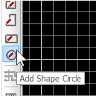
The use of the “Add Shape Circle” provides the required flexibility for this.
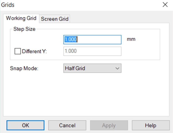
When creating a fiducial marker, proper grid configuration ensures accurate alignment and simplifies the design process. For a standard 1mm copper pad with a 3mm solder mask opening, follow these steps:
- Set Your Design Grid to 1mm
- This establishes a consistent reference scale for precise element placement.
- Enable Snap-to-Grid at 0.25mm or 0.5mm Increments
- Allows finer control when positioning the fiducial while maintaining alignment to the primary grid.
- Ensures perfect centering of the copper pad within the solder mask aperture.
- Implementation Benefits
- Guaranteed concentricity between copper and mask layers
- Efficient editing with automatic alignment to design rules
- Manufacturing-friendly output that avoids tolerance stacking issues
Pro Tip: For high-density designs, combine this approach with a 45° rotated grid when placing diagonal fiducial arrays to maintain optical recognition reliability.
This methodology is particularly valuable when working with:
- Laser-cut solder mask openings
- HDI designs requiring tight registration tolerances
- Panels with multiple fiducial marker arrays
Using this structured approach eliminates guesswork and ensures your fiducials meet IPC-7351 standards for machine vision recognition.
Key Advantages:
- Precision: Maintains perfect geometric relationships between layers
- Efficiency: Reduces design time with intelligent snapping
- Reliability: Produces manufacturing-ready fiducials in 3 quick steps
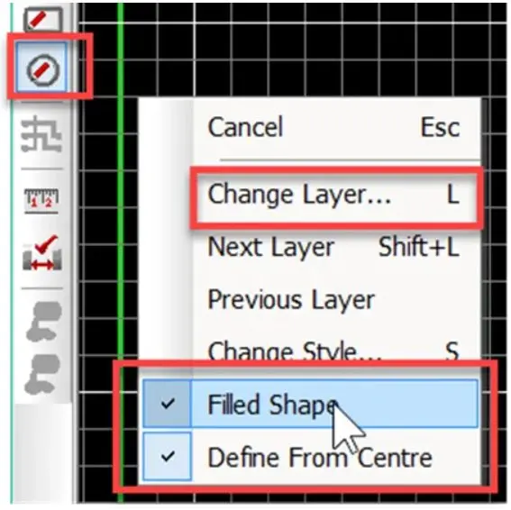
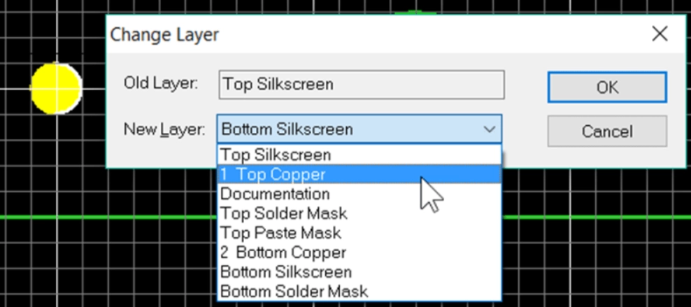
Select the “Add Shape Circle” and right-click before placing and ensure “Filled Shape” is set, you may also select the Layer or change layers after placing as shown.
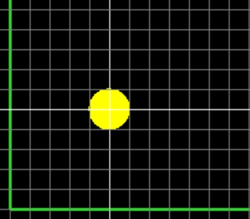
Place the circle shape and expand to the next half-grid line. Note grid setting in this example are 0.5mm.
If required then change the layer using the “L” key shortcut or select the object, right-click and select “Layers”. Change the layer to Top Copper.
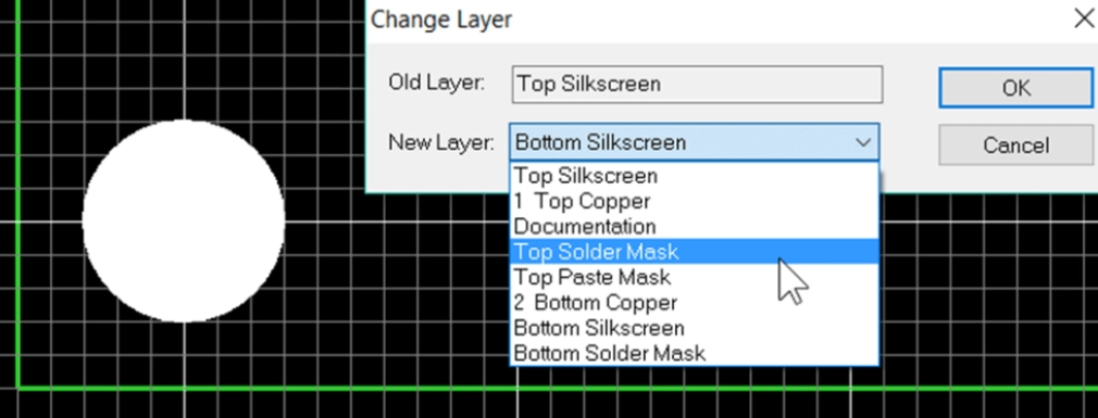
Repeat for solder mask exclusion area by adding another closed circle shape over the copper shape and change the layer to Top Solder Mask. The solder mask is a negative image, the shape will correspond to the excluded area of solder resist.
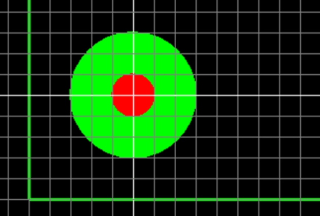
The fiducial is now created, use F5 to redraw the view.
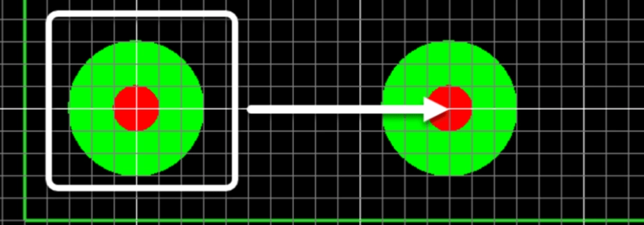
At this point it is good practice to select the fiducial, right click and select ‘Group’, this will prevent the copper circle and solder mask from becoming misaligned.
Further fiducials can be simply placed by selecting the fiducial and copying by CTRL+C and pasting by CTRL+V.
Although the fiducial cannot be saved as a library component a quick and easy solution for future use is to save the fiducial as a PCB design with the fiducial. When working on a new design also open this PCB design and you can copy and paste the fiducial to your current design as shown below.

PCB Fiducial Design Guidelines: Essential Rules for Machine Vision Accuracy
Fiducial markers require careful design to ensure reliable detection by assembly equipment. Follow these critical guidelines to optimize fiducial performance in your PCB layout.
1. Keep-Out Area Requirements
- Minimum Clearance Radius: At least 2× the fiducial diameter (per SMEMA 3.1)
- Example: A 1mm fiducial needs a 2mm clearance radius from copper traces/pours.
- Concentric Alignment: Fiducial and keep-out zones must share the same center point.
- Edge Clearance: Maintain >4.75mm (187 mils) from board edges to avoid pick-and-place clamp interference.
Why?
- Nearby copper or traces can reduce contrast, confusing machine vision.
- Clamps covering fiducials lead to assembly misalignment.
2. Fiducial Size & Consistency
Diameter Range: 1.00mm (40 mils) to 3.00mm (118 mils) (SMEMA standard).
- Size Matching: Fiducials must match within ±25µm (1 mil) across the PCB.
- Best Practice: Reuse the same fiducial padstack from your library to ensure uniformity.
3. Surface Finish & Protection
- Avoid Bare Copper: Oxidized/tarnished copper reduces optical contrast.
- Recommended Finishes:
- ENIG (Electroless Nickel Immersion Gold) – Best for long-term reliability.
- HASL (Hot Air Solder Leveling) – 5–10µm thickness (max 25µm).
- Solder Mask:
- Must be opened over the fiducial (no coverage).
- Glossy solder mask can cause reflections, interfering with machine vision.
4. Placement & Design Considerations
- Location: Typically placed in corners (global fiducials) or near high-precision components (local fiducials).
- Internal Layers: Suppress fiducial pads on non-essential layers (e.g., no inner-layer pads needed).
- Copper Pours: Allowed beneath fiducials (no electrical impact).
5. Best Practices for Manufacturing (DFM)
✅ Verify fiducial consistency in final design reviews.
✅ Use plated finishes (ENIG/HASL) to prevent oxidation.
✅ Avoid solder mask coverage—ensure proper mask opening.
✅ Check edge clearance to prevent clamp obstruction.
By following these rules, you ensure high assembly accuracy, fewer defects, and smoother automated production.