In the ever-evolving world of electronics manufacturing, quality control plays a crucial role in ensuring the reliability and functionality of printed circuit boards (PCBs). As PCB designs become increasingly complex and miniaturized, traditional inspection methods are often insufficient to detect all potential defects. This is where 3D Automated Optical Inspection (AOI) comes into play, revolutionizing the PCB assembly process with its advanced capabilities and precision.
3D AOI technology has emerged as a game-changer in the electronics industry, offering a comprehensive and highly accurate method for inspecting PCBs at various stages of production. By combining cutting-edge optical systems, sophisticated algorithms, and three-dimensional imaging techniques, 3D AOI systems can detect a wide range of defects that might otherwise go unnoticed until final testing or, worse, after the product reaches the end-user.
In this article, we will delve deep into the workings of 3D Automated Optical Inspection in the PCB assembly process. We’ll explore its core principles, key components, and the step-by-step procedure it follows to ensure the highest quality standards in PCB manufacturing. Additionally, we’ll discuss the advantages of 3D AOI over traditional inspection methods and its impact on production efficiency and product reliability.
Understanding 3D Automated Optical Inspection
What is 3D AOI?
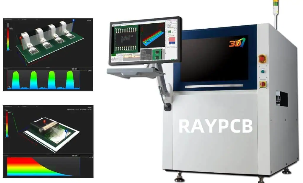
3D Automated Optical Inspection is an advanced quality control technique used in the PCB assembly process to detect and identify defects on printed circuit boards. Unlike traditional 2D AOI systems, which rely solely on top-down imaging, 3D AOI utilizes multiple cameras and advanced lighting techniques to create a three-dimensional representation of the PCB and its components.
This technology allows for a more comprehensive inspection, capable of detecting issues such as:
- Component placement errors
- Solder joint defects
- Missing or incorrect components
- Board warpage
- Component height variations
- Coplanarity issues
Key Components of a 3D AOI System
To understand how 3D AOI works, it’s essential to familiarize ourselves with its key components:
- Multiple High-Resolution Cameras: These capture images of the PCB from various angles.
- Structured Light Projectors: They project patterns onto the PCB surface to create 3D profiles.
- Advanced Lighting Systems: Including LED arrays and laser modules for optimal illumination.
- High-Speed Image Processing Unit: Analyzes the captured images in real-time.
- Sophisticated Software Algorithms: Interpret the data and identify defects based on predefined criteria.
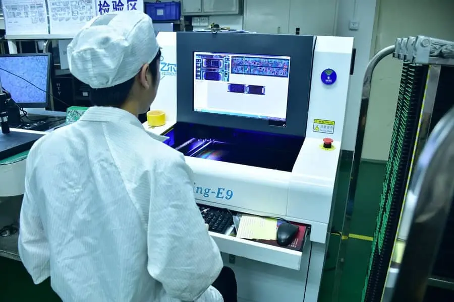
- Conveyor System: Moves PCBs through the inspection area.
- User Interface: Allows operators to configure settings and review inspection results.
The Evolution from 2D to 3D AOI
To appreciate the capabilities of 3D AOI, it’s helpful to understand its evolution from 2D systems:
| Aspect | 2D AOI | 3D AOI |
| Imaging | Single top-down view | Multiple angles and 3D profiling |
| Defect Detection | Surface-level defects | Surface and volumetric defects |
| Component Inspection | Limited to visible surfaces | Comprehensive, including hidden solder joints |
| Accuracy | Good for basic defects | Excellent, with reduced false calls |
| Solder Joint Inspection | Limited capability | Highly accurate and detailed |
| Coplanarity Checking | Not possible | Fully capable |
| Data Output | 2D images and measurements | 3D models and precise volumetric data |
This comparison highlights the significant advancements that 3D AOI brings to the PCB inspection process, enabling a more thorough and accurate quality control procedure.
The Working Principle of 3D AOI in PCB Assembly
Data Acquisition
The first step in the 3D AOI process is data acquisition. This phase involves capturing detailed images and creating a three-dimensional profile of the PCB under inspection. Here’s how it works:
- Multiple Camera Imaging: The PCB is photographed from various angles using high-resolution cameras. These images provide a comprehensive view of the board’s surface and components.
- Structured Light Projection: Patterns of light are projected onto the PCB surface. By analyzing how these patterns deform when projected onto three-dimensional objects, the system can create a detailed 3D map of the board.
- Laser Triangulation: In some systems, laser beams are used to measure the height and profile of components with high precision.
- Shadow Moiré Technology: This technique uses the interference patterns created by a reference grating and its shadow on the PCB to measure surface topography accurately.
The combination of these techniques allows the 3D AOI system to gather a wealth of data about the PCB’s physical characteristics, far beyond what is possible with traditional 2D inspection methods.
Image Processing and Analysis
Once the raw data is acquired, the 3D AOI system processes and analyzes it to identify potential defects. This stage involves several sophisticated algorithms and techniques:
- Image Enhancement: Raw images are processed to improve contrast, reduce noise, and highlight features of interest.
- 3D Reconstruction: The system combines data from multiple sources to create a detailed 3D model of the PCB.
- Feature Extraction: Key features such as component edges, solder joints, and pad locations are identified and isolated for further analysis.
- Pattern Matching: The observed features are compared against a database of known good examples or CAD data to identify discrepancies.
- Defect Classification: Any anomalies detected are classified into specific types of defects based on predefined criteria.
Defect Detection and Classification
The 3D AOI system is capable of detecting and classifying a wide range of defects. Here’s a table outlining some common defect types and how 3D AOI detects them:
| Defect Type | Detection Method |
| Component Misalignment | Comparison of actual vs. expected position in 3D space |
| Solder Joint Issues | Analysis of solder joint shape, volume, and surface characteristics |
| Missing Components | Absence of expected 3D features in component locations |
| Incorrect Components | Mismatch between observed and expected 3D profiles |
| Lifted Leads | Detection of abnormal height or angle of component leads |
| Tombstoning | Identification of components standing on end instead of lying flat |
| Solder Bridging | Detection of unexpected solder connections between pads |
| Insufficient Solder | Measurement of solder volume and coverage |
| Board Warpage | Analysis of overall PCB planarity |
| Foreign Object Debris | Identification of unexpected 3D objects on the board surface |
This comprehensive defect detection capability is one of the key advantages of 3D AOI over traditional inspection methods.
Result Reporting and Integration
After the inspection process, the 3D AOI system generates detailed reports of its findings. These reports typically include:
- High-resolution images of detected defects
- 3D renderings of problem areas
- Precise measurements and location data for each defect
- Statistical data on defect types and frequencies
Modern 3D AOI systems are often integrated into the broader manufacturing execution system (MES), allowing for real-time data sharing and process control. This integration enables:
- Immediate feedback to upstream processes for defect prevention
- Automatic routing of defective boards to repair stations
- Collection of long-term data for process improvement initiatives
- Traceability of individual boards throughout the manufacturing process
In the next section, we’ll explore the specific steps involved in setting up and operating a 3D AOI system in a PCB assembly line.